EP0314334A1 - Isolation of a charge coupled device - Google Patents
Isolation of a charge coupled device Download PDFInfo
- Publication number
- EP0314334A1 EP0314334A1 EP88309445A EP88309445A EP0314334A1 EP 0314334 A1 EP0314334 A1 EP 0314334A1 EP 88309445 A EP88309445 A EP 88309445A EP 88309445 A EP88309445 A EP 88309445A EP 0314334 A1 EP0314334 A1 EP 0314334A1
- Authority
- EP
- European Patent Office
- Prior art keywords
- die
- support member
- functional regions
- dielectric material
- functional
- Prior art date
- Legal status (The legal status is an assumption and is not a legal conclusion. Google has not performed a legal analysis and makes no representation as to the accuracy of the status listed.)
- Granted
Links
Images
Classifications
-
- H—ELECTRICITY
- H10—SEMICONDUCTOR DEVICES; ELECTRIC SOLID-STATE DEVICES NOT OTHERWISE PROVIDED FOR
- H10F—INORGANIC SEMICONDUCTOR DEVICES SENSITIVE TO INFRARED RADIATION, LIGHT, ELECTROMAGNETIC RADIATION OF SHORTER WAVELENGTH OR CORPUSCULAR RADIATION
- H10F39/00—Integrated devices, or assemblies of multiple devices, comprising at least one element covered by group H10F30/00, e.g. radiation detectors comprising photodiode arrays
- H10F39/10—Integrated devices
- H10F39/12—Image sensors
- H10F39/15—Charge-coupled device [CCD] image sensors
- H10F39/153—Two-dimensional or three-dimensional array CCD image sensors
-
- H—ELECTRICITY
- H10—SEMICONDUCTOR DEVICES; ELECTRIC SOLID-STATE DEVICES NOT OTHERWISE PROVIDED FOR
- H10W—GENERIC PACKAGES, INTERCONNECTIONS, CONNECTORS OR OTHER CONSTRUCTIONAL DETAILS OF DEVICES COVERED BY CLASS H10
- H10W10/00—Isolation regions in semiconductor bodies between components of integrated devices
- H10W10/01—Manufacture or treatment
- H10W10/021—Manufacture or treatment of air gaps
-
- H—ELECTRICITY
- H10—SEMICONDUCTOR DEVICES; ELECTRIC SOLID-STATE DEVICES NOT OTHERWISE PROVIDED FOR
- H10W—GENERIC PACKAGES, INTERCONNECTIONS, CONNECTORS OR OTHER CONSTRUCTIONAL DETAILS OF DEVICES COVERED BY CLASS H10
- H10W10/00—Isolation regions in semiconductor bodies between components of integrated devices
- H10W10/20—Air gaps
-
- H—ELECTRICITY
- H10—SEMICONDUCTOR DEVICES; ELECTRIC SOLID-STATE DEVICES NOT OTHERWISE PROVIDED FOR
- H10W—GENERIC PACKAGES, INTERCONNECTIONS, CONNECTORS OR OTHER CONSTRUCTIONAL DETAILS OF DEVICES COVERED BY CLASS H10
- H10W20/00—Interconnections in chips, wafers or substrates
- H10W20/40—Interconnections external to wafers or substrates, e.g. back-end-of-line [BEOL] metallisations or vias connecting to gate electrodes
-
- Y—GENERAL TAGGING OF NEW TECHNOLOGICAL DEVELOPMENTS; GENERAL TAGGING OF CROSS-SECTIONAL TECHNOLOGIES SPANNING OVER SEVERAL SECTIONS OF THE IPC; TECHNICAL SUBJECTS COVERED BY FORMER USPC CROSS-REFERENCE ART COLLECTIONS [XRACs] AND DIGESTS
- Y10—TECHNICAL SUBJECTS COVERED BY FORMER USPC
- Y10S—TECHNICAL SUBJECTS COVERED BY FORMER USPC CROSS-REFERENCE ART COLLECTIONS [XRACs] AND DIGESTS
- Y10S438/00—Semiconductor device manufacturing: process
- Y10S438/977—Thinning or removal of substrate
Definitions
- This invention relates to a method of treating an integrate circuit.
- a charge-coupled device may be made by processing a silicon wafer of p conductivity using conventional MOS technology to form a plurality of buried channels of n conductivity beneath the front surface of the wafer (the surface through which the wafer is processed). Each channel is made up of a linear array of like elementary zones.
- a clocking electrode structure overlies the front surface of the wafer, and by application of selected potentials to the clocking electrode structure, charge present in a given elementary zone of a channel may be advanced through the linear array of elementary zones, in the manner of a shift register, and extracted from the channel. Charge may be generated in the channels photoelectrically. Thus, if electromagnetic radiation enters the wafer it may cause generation of conduction electrons and these conduction electrons may become confined in one of the elementary channel zones.
- a known type of CCD has three distinct functional components formed in different regions of a single silicon die.
- the buried channels are formed in a channel region.
- the channel region is clocked between voltages of approximately 7-15 volts relative to the substrate, which is typically held at 0 volts.
- Charge that is propagated to the output ends of the buried channels is applied to an output amplifier which is formed in an amplifier region of the CCD.
- the output amplifier normally includes at least one field effect transistor.
- the substrate bias in the amplifer region is the same as that in the channel region.
- the field effect transistor of the output amplifier is generally operated with a large potential difference between the source and substrate and between the drain and substrate. This is required because the gate of the output transistor is connected to an output diode which is required to operate at a voltage of the order of 15 V.
- the large drain to substrate voltage causes the transistor to operate in an undesirable fashion.
- the large reverse bias on the drain causes light emission to occur from the junction. This light may propagate through the die of the known type of CCD and result in generation of conduction electrons in the buried channels, thus adding noise to the signals received by the output amplifer from the buried channels.
- the large drain to substrate bias forces the transistor, which is normally of the buried channel type, to operate in the surface channel mode. That is, the conduction channel, which normally would reside away from the silicon/silicon dioxide interface, is forced to the surface. This contributes additional noise to the output signal.
- level shifting amplifier it is known to use a level shifting amplifier to couple useful original information from a first circuit node at a first potential to a second circuit node at a second potential.
- level shifting amplifier it would not be practicable to use a level shifting amplifier to couple the output diode of a CCD to the gate of the output field effect transistor, because it would be the first amplifier in a chain of amplifiers and would inevitably introduce sub stantial noise into the output signal provided by the amplifier chain.
- the clock electrodes of the CCD are connected to clock drivers, which may be formed in a clock driver region of the wafer.
- the clock drivers are used to change the potentials of the clock electrodes at a high frequency, and therefore rapidly changing electric fields are generated by the clock drivers. In the known type of CCD, these fields are coupled through the die to the channel region, and influence the quantity of charge confined in the buried channels.
- a CCD may be used to generate a two-dimensionally sampled electrical signal representative of the distribution of light intensity over the channel region of the CCD.
- the thickness of the die be not much greater than the depth of the interface between the channels and the substrate. This may be achieved by securing the wafer at its front surface to a reinforcing member, and thinning the wafer from its back surface.
- a preferred embodiment of the present invention in its first aspect is a method of treating an integrated circuit formed in a semiconductor die having a front surface and a back surface, the die having at least two distinct functional regions comprising the steps of mounting the die by way of its front surface on a support member, and subsequently removing die material by way of the back surface so as to physically separate the functional regions of the die from each other.
- a preferred embodiment of the present invention in its second aspect is an integrated circuit which comprises a semiconductor die having front and back surfaces, the die having at least two distinct functional regions, and a support member attached to the front surface of the die, the different functional regions of the die being electrically isolated from each other.
- the CCD illustrated in FIG. 1 comprises a mono-crystalline die 2 of p conductivity having three distinct functional regions, namely, a channel region 10, a clock driver region 20, and an output amplifier region 30.
- a channel region 10 multiple parallel buried channels 12 of n conductivity are formed in the die.
- Each channel 12 ends in a floating diffusion 13 of n+ conductivity, which is also shown in FIG. 2A.
- a layer 14 (FIG. 2A) of thermally-grown silicon dioxide covers the buried channels 12.
- Three arrays of polysilicon clock electrodes 15, 16 and 17 extend over the silicon dioxide layer 14, perpendicular to the buried channels 12, and a further layer 18 (FIG.
- a metal interconnect strip 40 connects the electrode 19 to a bonding pad 42 which, as shown in FIG. 1, lies outside the channel region 10.
- the clock driver region 20 contains, integrated in the die, a circuit having input terminals which are connected by metal interconnect strips 44 (FIG. 1) to bonding pads 46, which lie outside the clock driver region 20, for connection to a power supply.
- the circuit also has output terminals connected to the clock electrode arrays 15, 16, and 17 respectively by metal interconnect strips 48.
- the output amplifier region 30 contains field effect transistors 31 of which the polysilicon gates 32, shown also in FIG. 2A, are connected by metal interconnect strips 49 to the floating diffusions 13 of the channels respectively.
- Each field effect transistor 31 has a source electrode 33, and pairs of adjacent FETs share a common drain electrode 34.
- a source diffusion 35, which lies out of the plane of FIG. 2A, is shown in dashed lines in FIG. 2A.
- the source and drain electrodes 33 and 34 are connected by metal interconnect strips 50 to respective metal bonding pads 52 outside the amplifier region 30. Ohmic contact is made to the die 2 inside the amplifier region 30 by a metal electrode (not shown) which is connected by a metal interconnect strip 55 to a bonding pad 56 which lies outside the region 30.
- the interconnect strips 40, 44, 48, 49, 50 and the bonding pads 42, 46, 53 are deposited on top of the silicon dioxide layer 18.
- a layer 60 (FIGS. 2 and 3) of high silica borosilicate glass is formed on top of the front surface of the die, and the die is thinned from its back surface to a thickness of about 10-20 m.
- the borosilicate glass which bonds firmly to the metal interconnect strips and bonding pads as well as to the silicon dioxide layer 18, reinforces the thinned substrate.
- the use of borosilicate glass as a reinforcing material for thinned CCDs is described in copending Patent Application Serial No. 07/018,832 filed February 24, 1987.
- the die is selectively etched from the back surface to the level of the silicon dioxide layer 14, to divide the die into three distinct portions, corresponding to the channel region 10, the clock driver region 20 and the output amplifier region 30 respectively.
- the etchant does not attack silicon dioxide, and therefore the layer 14 remains intact.
- a crystalline etch is performed, in which the etchant attacks the crystal planes parallel to the front surface of the die more strongly than it does other crystal planes.
- ethylene diamine pyrocatechol may be used as the etchant.
- a second etching operation is then carried out, using an etchant that attacks silicon dioxide but does not attack silicon or the metal employed for the interconnect strips and the bonding pads.
- the silicon dioxide of the layers 14 and 18 is removed where it covers the bonding pads 42. In this manner, the bonding pads are exposed. However, the oxide that covers the interconnect strips connecting the various regions of the die is masked so that the interconnect strips are not exposed.
- the etchant employed in the second etching operation attacks the material of the layer 60, but by controlling the time of the second etching operation removal of excessive material can be avoided.
- an optically opaque dielectric material 66 (FIG. 2B), such as a synthetic polymer material, may be placed in the trenches to ensure that no light would be propagated to the channel region from the output amplifier region or the clock driver region.
- the present invention is not restricted to the particular embodiment that has been described and illustrated, and that variations may be made therein without departing from the scope of the invention as defined in the appended claims and equivalents thereof.
- the invention is not limited to use with charge coupled devices.
- advanced CMOS tech nology in which diffusions are formed in a very thin epitaxial layer that has been grown on a monocrystalline wafer, the front surface of the epitaxial layer may be attached to a support member and the wafer on which the epitaxial layer was grown may be removed by etching. Different regions of the epitaxial layer may be separated from each other by trenches formed in the manner described with reference to FIG. 2.
- the invention is not limited to use with any particular material for the support member. It is necessary only that the coefficient of thermal expansion of the material of the support member match closely that of the wafer. Accordingly, in the case of a silicon wafer it is generally desirable that the material of the support member have a high silicon content.
Landscapes
- Solid State Image Pick-Up Elements (AREA)
- Element Separation (AREA)
- Weting (AREA)
Abstract
Description
- This invention relates to a method of treating an integrate circuit.
- A charge-coupled device (CCD) may be made by processing a silicon wafer of p conductivity using conventional MOS technology to form a plurality of buried channels of n conductivity beneath the front surface of the wafer (the surface through which the wafer is processed). Each channel is made up of a linear array of like elementary zones. A clocking electrode structure overlies the front surface of the wafer, and by application of selected potentials to the clocking electrode structure, charge present in a given elementary zone of a channel may be advanced through the linear array of elementary zones, in the manner of a shift register, and extracted from the channel. Charge may be generated in the channels photoelectrically. Thus, if electromagnetic radiation enters the wafer it may cause generation of conduction electrons and these conduction electrons may become confined in one of the elementary channel zones.
- A known type of CCD has three distinct functional components formed in different regions of a single silicon die. The buried channels are formed in a channel region. In operation, the channel region is clocked between voltages of approximately 7-15 volts relative to the substrate, which is typically held at 0 volts. Charge that is propagated to the output ends of the buried channels is applied to an output amplifier which is formed in an amplifier region of the CCD. The output amplifier normally includes at least one field effect transistor. In the known type of CCD the substrate bias in the amplifer region is the same as that in the channel region.
- The field effect transistor of the output amplifier is generally operated with a large potential difference between the source and substrate and between the drain and substrate. This is required because the gate of the output transistor is connected to an output diode which is required to operate at a voltage of the order of 15 V. The large drain to substrate voltage causes the transistor to operate in an undesirable fashion. First, the large reverse bias on the drain causes light emission to occur from the junction. This light may propagate through the die of the known type of CCD and result in generation of conduction electrons in the buried channels, thus adding noise to the signals received by the output amplifer from the buried channels. Second, the large drain to substrate bias forces the transistor, which is normally of the buried channel type, to operate in the surface channel mode. That is, the conduction channel, which normally would reside away from the silicon/silicon dioxide interface, is forced to the surface. This contributes additional noise to the output signal.
- It is known to use a level shifting amplifier to couple useful original information from a first circuit node at a first potential to a second circuit node at a second potential. However, it would not be practicable to use a level shifting amplifier to couple the output diode of a CCD to the gate of the output field effect transistor, because it would be the first amplifier in a chain of amplifiers and would inevitably introduce sub stantial noise into the output signal provided by the amplifier chain.
- The clock electrodes of the CCD are connected to clock drivers, which may be formed in a clock driver region of the wafer. The clock drivers are used to change the potentials of the clock electrodes at a high frequency, and therefore rapidly changing electric fields are generated by the clock drivers. In the known type of CCD, these fields are coupled through the die to the channel region, and influence the quantity of charge confined in the buried channels.
- A CCD may be used to generate a two-dimensionally sampled electrical signal representative of the distribution of light intensity over the channel region of the CCD. In such an imaging CCD, it is desirable that the thickness of the die be not much greater than the depth of the interface between the channels and the substrate. This may be achieved by securing the wafer at its front surface to a reinforcing member, and thinning the wafer from its back surface.
- A preferred embodiment of the present invention in its first aspect is a method of treating an integrated circuit formed in a semiconductor die having a front surface and a back surface, the die having at least two distinct functional regions comprising the steps of mounting the die by way of its front surface on a support member, and subsequently removing die material by way of the back surface so as to physically separate the functional regions of the die from each other.
- A preferred embodiment of the present invention in its second aspect is an integrated circuit which comprises a semiconductor die having front and back surfaces, the die having at least two distinct functional regions, and a support member attached to the front surface of the die, the different functional regions of the die being electrically isolated from each other.
- For a better understanding of the invention, and to show how the same may be carried into effect, reference will now be made, by way of example, to the accompanying drawings in which:
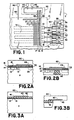
- FIG. 1 is a diagrammatic view of the front surface of an imaging CCD,
- FIGS. 2A and 2B are partial sectional views of one part of the CCD at two stages in the fabrication thereof, and
- FIGS. 3A and 3B are partial sectional views of another part of the CCD at the two fabrication stages shown in FIGS. 2A and 2B respectively.
- The CCD illustrated in FIG. 1 comprises a mono-
crystalline die 2 of p conductivity having three distinct functional regions, namely, achannel region 10, aclock driver region 20, and anoutput amplifier region 30. In thechannel region 10, multiple parallel buriedchannels 12 of n conductivity are formed in the die. Eachchannel 12 ends in afloating diffusion 13 of n+ conductivity, which is also shown in FIG. 2A. A layer 14 (FIG. 2A) of thermally-grown silicon dioxide covers the buriedchannels 12. Three arrays ofpolysilicon clock electrodes silicon dioxide layer 14, perpendicular to the buriedchannels 12, and a further layer 18 (FIG. 2A) of silicon dioxide, formed by a reflow operation, covers the clock electrode arrays. Ohmic contact is made to the die 2 inside thechannel region 10 by a metal electrode 19 (FIG. 3A). Ametal interconnect strip 40 connects theelectrode 19 to abonding pad 42 which, as shown in FIG. 1, lies outside thechannel region 10. - The
clock driver region 20 contains, integrated in the die, a circuit having input terminals which are connected by metal interconnect strips 44 (FIG. 1) to bondingpads 46, which lie outside theclock driver region 20, for connection to a power supply. The circuit also has output terminals connected to theclock electrode arrays metal interconnect strips 48. - The
output amplifier region 30 containsfield effect transistors 31 of which thepolysilicon gates 32, shown also in FIG. 2A, are connected bymetal interconnect strips 49 to thefloating diffusions 13 of the channels respectively. Eachfield effect transistor 31 has asource electrode 33, and pairs of adjacent FETs share acommon drain electrode 34. Asource diffusion 35, which lies out of the plane of FIG. 2A, is shown in dashed lines in FIG. 2A. The source anddrain electrodes metal interconnect strips 50 to respectivemetal bonding pads 52 outside theamplifier region 30. Ohmic contact is made to thedie 2 inside theamplifier region 30 by a metal electrode (not shown) which is connected by ametal interconnect strip 55 to abonding pad 56 which lies outside theregion 30. - The
interconnect strips bonding pads silicon dioxide layer 18. - A layer 60 (FIGS. 2 and 3) of high silica borosilicate glass is formed on top of the front surface of the die, and the die is thinned from its back surface to a thickness of about 10-20 m. The borosilicate glass, which bonds firmly to the metal interconnect strips and bonding pads as well as to the
silicon dioxide layer 18, reinforces the thinned substrate. The use of borosilicate glass as a reinforcing material for thinned CCDs is described in copending Patent Application Serial No. 07/018,832 filed February 24, 1987. - Using conventional photoprocessing techniques, the die is selectively etched from the back surface to the level of the
silicon dioxide layer 14, to divide the die into three distinct portions, corresponding to thechannel region 10, theclock driver region 20 and theoutput amplifier region 30 respectively. The etchant does not attack silicon dioxide, and therefore thelayer 14 remains intact. Preferably, a crystalline etch is performed, in which the etchant attacks the crystal planes parallel to the front surface of the die more strongly than it does other crystal planes. For example, if, as is conventional in fabrication of integrated circuits, the front surface is parallel to the 100 crystal plane, ethylene diamine pyrocatechol may be used as the etchant. A second etching operation is then carried out, using an etchant that attacks silicon dioxide but does not attack silicon or the metal employed for the interconnect strips and the bonding pads. In this second etching operation, the silicon dioxide of thelayers bonding pads 42. In this manner, the bonding pads are exposed. However, the oxide that covers the interconnect strips connecting the various regions of the die is masked so that the interconnect strips are not exposed. The etchant employed in the second etching operation attacks the material of thelayer 60, but by controlling the time of the second etching operation removal of excessive material can be avoided. By thus dividing the die into discrete portions, corresponding respectively to the functional regions of the die, it becomes possible to employ different substrate bias voltages for the output amplifier region and for the channel region respectively. Similarly, the rapidly changing fields in the clock driver region are not coupled through the die to the channel region. Light generated by operation of the transistors in the output amplifier region and the clock driver region is not propagated so readily to the channel region, due to reflection and scattering at the walls of the trenches formed by etching. In any event, an optically opaque dielectric material 66 (FIG. 2B), such as a synthetic polymer material, may be placed in the trenches to ensure that no light would be propagated to the channel region from the output amplifier region or the clock driver region. - It will be appreciated that the present invention is not restricted to the particular embodiment that has been described and illustrated, and that variations may be made therein without departing from the scope of the invention as defined in the appended claims and equivalents thereof. For example, the invention is not limited to use with charge coupled devices. In advanced CMOS tech nology, in which diffusions are formed in a very thin epitaxial layer that has been grown on a monocrystalline wafer, the front surface of the epitaxial layer may be attached to a support member and the wafer on which the epitaxial layer was grown may be removed by etching. Different regions of the epitaxial layer may be separated from each other by trenches formed in the manner described with reference to FIG. 2. Moreover, the invention is not limited to use with any particular material for the support member. It is necessary only that the coefficient of thermal expansion of the material of the support member match closely that of the wafer. Accordingly, in the case of a silicon wafer it is generally desirable that the material of the support member have a high silicon content.
Claims (9)
mounting the die by way of its front face on a support member, and
removing material of the die by way of the back face so as to separate the functional regions of the die from each other.
a support member, and
a semiconductor die having front and back faces and being attached at its front face to the support member, the die having at least two distinct functional regions which are electrically isolated from each other.
Applications Claiming Priority (2)
| Application Number | Priority Date | Filing Date | Title |
|---|---|---|---|
| US114884 | 1987-10-29 | ||
| US07/114,884 US4892842A (en) | 1987-10-29 | 1987-10-29 | Method of treating an integrated circuit |
Publications (2)
| Publication Number | Publication Date |
|---|---|
| EP0314334A1 true EP0314334A1 (en) | 1989-05-03 |
| EP0314334B1 EP0314334B1 (en) | 1995-03-15 |
Family
ID=22358002
Family Applications (1)
| Application Number | Title | Priority Date | Filing Date |
|---|---|---|---|
| EP88309445A Expired - Lifetime EP0314334B1 (en) | 1987-10-29 | 1988-10-10 | Isolation of a charge coupled device |
Country Status (5)
| Country | Link |
|---|---|
| US (1) | US4892842A (en) |
| EP (1) | EP0314334B1 (en) |
| JP (1) | JP2520288B2 (en) |
| CA (1) | CA1291579C (en) |
| DE (1) | DE3853335T2 (en) |
Cited By (2)
| Publication number | Priority date | Publication date | Assignee | Title |
|---|---|---|---|---|
| GB2221092B (en) * | 1988-07-19 | 1992-06-03 | Tektronix Inc | Integrated circuit and method of treating an integrated circuit |
| EP0836231A3 (en) * | 1996-10-11 | 1998-11-11 | Hamamatsu Photonics K.K. | Back irradiation type light-receiving device and method of making the same |
Families Citing this family (9)
| Publication number | Priority date | Publication date | Assignee | Title |
|---|---|---|---|---|
| US5162251A (en) * | 1991-03-18 | 1992-11-10 | Hughes Danbury Optical Systems, Inc. | Method for making thinned charge-coupled devices |
| JP3246129B2 (en) * | 1993-10-01 | 2002-01-15 | ソニー株式会社 | Method for manufacturing semiconductor device |
| US5387536A (en) * | 1994-01-26 | 1995-02-07 | Eastman Kodak Company | Method of making a low capacitance floating diffusion structure for a solid state image sensor |
| US5508231A (en) * | 1994-03-07 | 1996-04-16 | National Semiconductor Corporation | Apparatus and method for achieving mechanical and thermal isolation of portions of integrated monolithic circuits |
| KR100380701B1 (en) * | 1994-07-26 | 2003-07-22 | 코닌클리케 필립스 일렉트로닉스 엔.브이. | Manufacturing Method of Surface Mount Semiconductor Device and Semiconductor Device for Surface Mount |
| US5807783A (en) * | 1996-10-07 | 1998-09-15 | Harris Corporation | Surface mount die by handle replacement |
| US5915167A (en) * | 1997-04-04 | 1999-06-22 | Elm Technology Corporation | Three dimensional structure memory |
| US6551857B2 (en) * | 1997-04-04 | 2003-04-22 | Elm Technology Corporation | Three dimensional structure integrated circuits |
| US8933715B2 (en) | 2012-04-08 | 2015-01-13 | Elm Technology Corporation | Configurable vertical integration |
Citations (4)
| Publication number | Priority date | Publication date | Assignee | Title |
|---|---|---|---|---|
| FR2025015A7 (en) * | 1968-12-02 | 1970-09-04 | Telefunken Gmbh | |
| US3665263A (en) * | 1970-06-05 | 1972-05-23 | Katsuhiko Akiyama | Improvements in air-isolated integrated circuit devices to facilitate the connection thereof to circuit boards |
| US4106046A (en) * | 1977-01-26 | 1978-08-08 | Westinghouse Electric Corp. | Radiant energy sensor |
| EP0001707A1 (en) * | 1977-10-17 | 1979-05-02 | John Fluke Mfg. Co., Inc. | A thermally isolated monolithic semiconductor die and a process for producing such a die |
Family Cites Families (14)
| Publication number | Priority date | Publication date | Assignee | Title |
|---|---|---|---|---|
| US3508980A (en) * | 1967-07-26 | 1970-04-28 | Motorola Inc | Method of fabricating an integrated circuit structure with dielectric isolation |
| US3623219A (en) * | 1969-10-22 | 1971-11-30 | Rca Corp | Method for isolating semiconductor devices from a wafer of semiconducting material |
| JPS5312917B2 (en) * | 1972-06-02 | 1978-05-06 | ||
| US3875657A (en) * | 1973-09-04 | 1975-04-08 | Trw Inc | Dielectrically isolated semiconductor devices |
| US3911559A (en) * | 1973-12-10 | 1975-10-14 | Texas Instruments Inc | Method of dielectric isolation to provide backside collector contact and scribing yield |
| US4050979A (en) * | 1973-12-28 | 1977-09-27 | Texas Instruments Incorporated | Process for thinning silicon with special application to producing silicon on insulator |
| JPS52116085A (en) * | 1976-03-26 | 1977-09-29 | Hitachi Ltd | Air-space semiconductor integrated circuit |
| JPS5330284A (en) * | 1976-09-01 | 1978-03-22 | Hitachi Ltd | Production of substrate for semiconductor integrated circuits |
| GB2137807B (en) * | 1983-04-05 | 1987-08-12 | Plessey Co Plc | A semiconductor component and method of manufacture |
| JPS60165737A (en) * | 1984-02-08 | 1985-08-28 | Hitachi Ltd | Dielectric isolation substrate |
| JPS618940A (en) * | 1984-06-25 | 1986-01-16 | Nec Corp | Manufacture of semiconductor device |
| JPS6159824A (en) * | 1984-08-31 | 1986-03-27 | Fujitsu Ltd | Manufacture of semiconductor element |
| KR970000416B1 (en) * | 1985-05-31 | 1997-01-09 | 사이언티픽 이매징 테크놀로지시 이코포레이티드 | Silicon Wafer Reinforcement and Reinforcement Method |
| JPS61296736A (en) * | 1985-06-25 | 1986-12-27 | Matsushita Electric Works Ltd | Manufacture of dielectric isolation substrate |
-
1987
- 1987-10-29 US US07/114,884 patent/US4892842A/en not_active Expired - Lifetime
-
1988
- 1988-10-10 DE DE3853335T patent/DE3853335T2/en not_active Expired - Fee Related
- 1988-10-10 EP EP88309445A patent/EP0314334B1/en not_active Expired - Lifetime
- 1988-10-21 JP JP63265951A patent/JP2520288B2/en not_active Expired - Fee Related
- 1988-10-25 CA CA000581232A patent/CA1291579C/en not_active Expired - Fee Related
Patent Citations (4)
| Publication number | Priority date | Publication date | Assignee | Title |
|---|---|---|---|---|
| FR2025015A7 (en) * | 1968-12-02 | 1970-09-04 | Telefunken Gmbh | |
| US3665263A (en) * | 1970-06-05 | 1972-05-23 | Katsuhiko Akiyama | Improvements in air-isolated integrated circuit devices to facilitate the connection thereof to circuit boards |
| US4106046A (en) * | 1977-01-26 | 1978-08-08 | Westinghouse Electric Corp. | Radiant energy sensor |
| EP0001707A1 (en) * | 1977-10-17 | 1979-05-02 | John Fluke Mfg. Co., Inc. | A thermally isolated monolithic semiconductor die and a process for producing such a die |
Non-Patent Citations (1)
| Title |
|---|
| IBM TECHNICAL DISCLOSURE BULLETIN, vol. 27, no. 4A, September 1984, pages 1836-1837, New York, US; J. GRESCHNER et al.: "Method of evenly filling isolation trenches" * |
Cited By (3)
| Publication number | Priority date | Publication date | Assignee | Title |
|---|---|---|---|---|
| GB2221092B (en) * | 1988-07-19 | 1992-06-03 | Tektronix Inc | Integrated circuit and method of treating an integrated circuit |
| EP0836231A3 (en) * | 1996-10-11 | 1998-11-11 | Hamamatsu Photonics K.K. | Back irradiation type light-receiving device and method of making the same |
| US6031274A (en) * | 1996-10-11 | 2000-02-29 | Hamamatsu Photonics K.K. | Back irradiation type light-receiving device and method of making the same |
Also Published As
| Publication number | Publication date |
|---|---|
| JP2520288B2 (en) | 1996-07-31 |
| JPH01154559A (en) | 1989-06-16 |
| CA1291579C (en) | 1991-10-29 |
| US4892842A (en) | 1990-01-09 |
| DE3853335D1 (en) | 1995-04-20 |
| EP0314334B1 (en) | 1995-03-15 |
| DE3853335T2 (en) | 1995-07-27 |
Similar Documents
| Publication | Publication Date | Title |
|---|---|---|
| US4948748A (en) | Manufacture of a substrate structure for a composite semiconductor device using wafer bonding and epitaxial refill | |
| US4199777A (en) | Semiconductor device and a method of manufacturing the same | |
| US4033797A (en) | Method of manufacturing a complementary metal-insulation-semiconductor circuit | |
| US4984045A (en) | Output sensor of charge transfer device | |
| US4892842A (en) | Method of treating an integrated circuit | |
| US4859624A (en) | Manufacturing method of semiconductor device having CCD and peripheral circuit | |
| JP2998662B2 (en) | Semiconductor device | |
| US5714796A (en) | Integrated circuit device fabricated on semiconductor substrate blocking power supply lines from noise | |
| EP0114491B1 (en) | Semiconductor integrated circuit device with output stage | |
| US20100072627A1 (en) | Wafer including intercepting through-vias and method of making intercepting through-vias in a wafer | |
| KR100325497B1 (en) | Dielectric Separation Semiconductor Device | |
| KR100285002B1 (en) | Semiconductor device and manufacturing method thereof | |
| US7339249B2 (en) | Semiconductor device | |
| US4923825A (en) | Method of treating a semiconductor body | |
| US6472699B1 (en) | Photoelectric transducer and manufacturing method of the same | |
| JPH07106553A (en) | Solid state image pickup element | |
| JPH01111376A (en) | charge coupled device | |
| KR20060094288A (en) | SOS-en MOS transistor using beam structure, inverter device using same and manufacturing method thereof | |
| KR100396636B1 (en) | Method for producing field effect transistors in integrated semiconductor circuits and semiconductor circuit with such a field effect transistor | |
| KR20000057834A (en) | Semiconductor device | |
| JPS6334949A (en) | Semiconductor device | |
| JPS6124245A (en) | Semiconductor device | |
| JPH07118535B2 (en) | Charge transfer device and driving method thereof | |
| JPS59198755A (en) | Solid-state image sensor and its manufacturing method | |
| JPH06275833A (en) | Semiconductor device |
Legal Events
| Date | Code | Title | Description |
|---|---|---|---|
| PUAI | Public reference made under article 153(3) epc to a published international application that has entered the european phase |
Free format text: ORIGINAL CODE: 0009012 |
|
| AK | Designated contracting states |
Kind code of ref document: A1 Designated state(s): DE FR GB NL |
|
| 17P | Request for examination filed |
Effective date: 19891017 |
|
| 17Q | First examination report despatched |
Effective date: 19920730 |
|
| RAP1 | Party data changed (applicant data changed or rights of an application transferred) |
Owner name: SCIENTIFIC IMAGING TECHNOLOGIES, INC. |
|
| GRAA | (expected) grant |
Free format text: ORIGINAL CODE: 0009210 |
|
| AK | Designated contracting states |
Kind code of ref document: B1 Designated state(s): DE FR GB NL |
|
| ET | Fr: translation filed | ||
| REF | Corresponds to: |
Ref document number: 3853335 Country of ref document: DE Date of ref document: 19950420 |
|
| PLBE | No opposition filed within time limit |
Free format text: ORIGINAL CODE: 0009261 |
|
| STAA | Information on the status of an ep patent application or granted ep patent |
Free format text: STATUS: NO OPPOSITION FILED WITHIN TIME LIMIT |
|
| 26N | No opposition filed | ||
| REG | Reference to a national code |
Ref country code: GB Ref legal event code: IF02 |
|
| PGFP | Annual fee paid to national office [announced via postgrant information from national office to epo] |
Ref country code: FR Payment date: 20041111 Year of fee payment: 17 |
|
| PGFP | Annual fee paid to national office [announced via postgrant information from national office to epo] |
Ref country code: NL Payment date: 20041115 Year of fee payment: 17 |
|
| PGFP | Annual fee paid to national office [announced via postgrant information from national office to epo] |
Ref country code: GB Payment date: 20041116 Year of fee payment: 17 |
|
| PGFP | Annual fee paid to national office [announced via postgrant information from national office to epo] |
Ref country code: DE Payment date: 20041117 Year of fee payment: 17 |
|
| PG25 | Lapsed in a contracting state [announced via postgrant information from national office to epo] |
Ref country code: GB Free format text: LAPSE BECAUSE OF NON-PAYMENT OF DUE FEES Effective date: 20051010 |
|
| PG25 | Lapsed in a contracting state [announced via postgrant information from national office to epo] |
Ref country code: NL Free format text: LAPSE BECAUSE OF NON-PAYMENT OF DUE FEES Effective date: 20060501 |
|
| PG25 | Lapsed in a contracting state [announced via postgrant information from national office to epo] |
Ref country code: DE Free format text: LAPSE BECAUSE OF NON-PAYMENT OF DUE FEES Effective date: 20060503 |
|
| GBPC | Gb: european patent ceased through non-payment of renewal fee |
Effective date: 20051010 |
|
| PG25 | Lapsed in a contracting state [announced via postgrant information from national office to epo] |
Ref country code: FR Free format text: LAPSE BECAUSE OF NON-PAYMENT OF DUE FEES Effective date: 20060630 |
|
| NLV4 | Nl: lapsed or anulled due to non-payment of the annual fee |
Effective date: 20060501 |
|
| REG | Reference to a national code |
Ref country code: FR Ref legal event code: ST Effective date: 20060630 |