EP0315550A2 - Hochparallele Rechnerbauweise unter Verwendung eines Koordinatenschalters mit ausgewählter Pipelineverzögerung - Google Patents
Hochparallele Rechnerbauweise unter Verwendung eines Koordinatenschalters mit ausgewählter Pipelineverzögerung Download PDFInfo
- Publication number
- EP0315550A2 EP0315550A2 EP88402787A EP88402787A EP0315550A2 EP 0315550 A2 EP0315550 A2 EP 0315550A2 EP 88402787 A EP88402787 A EP 88402787A EP 88402787 A EP88402787 A EP 88402787A EP 0315550 A2 EP0315550 A2 EP 0315550A2
- Authority
- EP
- European Patent Office
- Prior art keywords
- crossbar switch
- memory
- recited
- crossbar
- data
- Prior art date
- Legal status (The legal status is an assumption and is not a legal conclusion. Google has not performed a legal analysis and makes no representation as to the accuracy of the status listed.)
- Ceased
Links
Images


Classifications
-
- G—PHYSICS
- G06—COMPUTING OR CALCULATING; COUNTING
- G06F—ELECTRIC DIGITAL DATA PROCESSING
- G06F15/00—Digital computers in general; Data processing equipment in general
- G06F15/16—Combinations of two or more digital computers each having at least an arithmetic unit, a program unit and a register, e.g. for a simultaneous processing of several programs
- G06F15/163—Interprocessor communication
- G06F15/173—Interprocessor communication using an interconnection network, e.g. matrix, shuffle, pyramid, star, snowflake
- G06F15/17356—Indirect interconnection networks
- G06F15/17368—Indirect interconnection networks non hierarchical topologies
- G06F15/17375—One dimensional, e.g. linear array, ring
-
- G—PHYSICS
- G06—COMPUTING OR CALCULATING; COUNTING
- G06F—ELECTRIC DIGITAL DATA PROCESSING
- G06F9/00—Arrangements for program control, e.g. control units
- G06F9/06—Arrangements for program control, e.g. control units using stored programs, i.e. using an internal store of processing equipment to receive or retain programs
- G06F9/30—Arrangements for executing machine instructions, e.g. instruction decode
- G06F9/38—Concurrent instruction execution, e.g. pipeline or look ahead
- G06F9/3885—Concurrent instruction execution, e.g. pipeline or look ahead using a plurality of independent parallel functional units
Definitions
- the present invention relates to a supercomputer and, more specifically, to a crossbar switch for a very high speed, large grain computer node system incorporating a highly parallel architecture.
- Supercomputers are typically defined as computers capable of executing 100 million floating point operations per second (MFLOPS).
- Conventional supercomputers such as the Cray supercomputer, achieve this phenomenal performance by using an extremely fast clock, on the order of 4 ns per cycle.
- Unfortunately such a high-speed clock generates a considerable amount of heat, which requires that such supercomputers remain submerged in liquid for cooling purposes.
- the design of conventional supercomputers also requires a large physical size for housing a large amount of hardware, such that these units typically occupy a small room. Accordingly, such supercomputers are essentially limited to laboratory applications.
- the present invention overcomes the forementioned drawbacks by the provision of a unique, highly parallel architecture comprising a plurality of processor nodes, each having a novel crossbar switch which allows any one of a plurality of floating point arithmetic units in each processor node to communicate with any one of a plurality of parallel memory modules.
- the configuration of the crossbar switch i.e., the connection between each floating point arithmetic unit and each parallel memory module, may be changed dynamically on a cycle-by-cycle basis in accordance with the algorithm being executed.
- the data is distributed over memory such that, for a given algorithm, the floating point arithmetic units can access and operate on data in a highly parallel fashion to achieve supercomputer performance.
- the crossbar switch which allows the highly parallel operation is comprised of two basic sections : a multiplexer and a control section.
- the multiplexer provides the actual switching of signal paths, i.e., connects each floating point arithmetic unit to a particular parallel memory on each clock cycle.
- the control section determines which connections are made on each clock cycle in accordance with the algorithm under execution.
- a selectable pipelined delay in the circuitry of the control section provides optimal data transfer efficiency between the processors and memory modules over a wide range of array processing algorithms using interlaced memory reads and writes over a parallel bidirectional data bus.
- the highly parallel architecture of the present invention allows true supercomputer performance to be achieved with a clock which runs at conventional PC clock rates of 100 ns per cycle.
- the supercomputer of the present invention does not generate excessive heat during operation and may be air cooled.
- the unique architecture of the present invention employs "off the shelf” components arranged in a stand alone unit of about one-third the size of conventional supercomputers. This feature, along with air cooling, allows the supercomputer of the present invention to be used in a variety of applications outside the laboratory heretofore impossible with such computing power.
- the highly parallel structure of the invention also allows most component failures to be bypassed by re- configuring the processing node through the crossbar switch, such that only operational components are used, while fault detection is performed on a failed section.
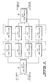
- FIG. 1 The overall system architecture of a processor node 1 is shown in Fig. 1.
- a plurality of floating point arithmetic units (FPAU) 2 are connected through a crossbar switch (XBAR) 4 to a plurality of parallel memories (PMEM) 6.
- the crossbar switch 4 of the present invention which is described in further detail below, advantageously allows any FPAU 2 to be connected to any PMEM 6.
- the processor node of the present invention comprises a 160 MFLOP system configuration.
- the processor nodes 1 can be networked together, each node being connected to its nearest neighboring nodes and to a common input-output processor 8.
- Fig. 2 shows an eight node configuration, in the preferred embodiment 64 processor nodes 1 are networked together to increase the system throughput to 10,000 MFLOPS, such that real-time operation for applications involving intensive computation and high bandwidth input/output is possible.
- the present invention is the first system of such power which is air-cooled and thus has the ability to be installed on ruggedized moveable platforms such as ships and planes.
- the host processor 10 is common to all processor nodes 1 and controls the configuration and feed of the nodes by communicating and downloading information to a micro controller executive 12 in each node.
- the host processor 10 also runs a flow graph editor and flow compiler (not shown), which provide for human interface with the system.
- the internal node architecture includes a micro controller executive 12, which monitors and schedules tasks within each node and coordinates the input and output of each node to and from its nearest neighbor nodes.
- Each processor node is constructed modularly to allow incremental adjustment of "number crunching" power.
- each of the nodes can provide between 20 and 160 MFLOPS of computing power.
- the unique architecture of the present invention also achieves the following performance characteristics per node : - a bus bandwidth of 80 million words per second is achieved when all 8 FPAU's are continuously reading from or writing to all 8 PMEM memories.
- the algorithms which control the switching of the crossbar are designed for maximum usage of system hardware. For most algorithms, the percentage of full bas bandwidth achieved during algorithm execution is nearly 100%.
- a system performance of 80 million instructions per second is attained through the use of eight fully synchronized, concurrently running FPAU's, each of which is continuously executing at a rate of 10 million instructions per second.
- Each FPAU is capable of performing 2 floating point operations (any combination of multiplies & adds) and one fixed point arithmetic/logic operation per instruction cycle. If all FPAU's are concurrently performing floating point operations at their peak rates, then a total system throughput of 160 MFLOP can be achieved. In practice, the number of floating point operations performed is dependent on the algorithm being executed. For example, the radix-2 FFT algorithm, which transfers data to and from memory at the peak rate of 80 million words per second, requires an arithmetic throughput of only 120 MFLOP. As a second example, a convolution algorithm transfers data to and from memory at nearly 100% of full bus bandwidth, and it also performs arithmetic at nearly 100% of peak MFLOP rating.
- the processor of the present invention achieves its high performance over a wide range of signal processing algorithms through the use of a novel crossbar switch (XBAR) 4.
- the XBAR allows each of up to 8 FPAU's to extend their address, data and read/write control buses to any one of up to 8 different memory modules (PMEM's) ; the memory selected by an individual FPAU can be changed dynamically on a cycle-by-cycle basis. No more than one FPAU can write to the same memory during the same bus transfer cycle. Howevever, all FPAU's may read from the same address of any single memory during what is referred to as a "broadcast read" cycle. In order to avoid bus clash, the signal processing algorithms must be developed so that these rules are not violated.
- the processor is run by upper level language callable subroutines of standard vector processor types such as the Fast Fourier Transform (FFT), Matrix Inversion, Singular Value algorithms such as adaptive filtering and image enhancement.
- FFT Fast Fourier Transform
- Matrix Inversion Matrix Inversion
- Singular Value algorithms such as adaptive filtering and image enhancement.
- System resources are allocated by the host 10 to assure that maximum throughput occurs thus minimizing any possible resource idling. If the use of the host 10 as an operator interface is not desired, it can be disconnected. The output of the host 10 can then be burned into PROM located in the executive controller 12 for embedded applications such as sonar or radar.
- any single algorithm such as the FFT
- all FPAU's are programmed to concurrently perform their own portion of the algorithm. Once an algorithm is developed,it may then be used in any application without the need for any additional planning of crossbar utilization. In other words, once a family of signal processing algorithms has been developed, the XBAR 4 becomes transparent to any subsequent applications utilizing these processing algorithms, and the 8 FPAU's appear to the user as one single processor with 8 times the performance of the individual FPAU's.
- Memory selection among the PMEM's is accomplished by decoding the three least significant bits of the address output from each of the FPAU's. If all 8 FPAU's are concurrently performing a memory access (other than a broadcast read, described above), the three LSB's of their respective output addresses must all be unique in order to obey the crossbar usage rule.
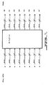
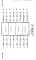
- FIG. 3 A memory address mapping diagram is presented in Fig. 3. Each of the eight columns represents a different physical memory, and the number inside each cell of any column is the address value required to access that cell of memory.
- the mapping pattern of data vectors and matrices into memory is presented in Figs. 4 and 5, respectively. Note that vectors and matrix rows are distributed over all memories. Each matrix column, on the other hand, is completely contained in one of the 8 memories.
- the crossbar rules can now be explained in relation to these data types.
- vectors For one dimensional data arrays (vectors), more than one FPAU cannot concurrently access the same vector element, nor can the FPAU's concurrently access vector elements which are displaced from one another by integer multiples of eight locations.
- more than one FPAU cannot concurrently access any elements either from the same column vector of from column vectors which are displaced from one another by integer multiples of 8 columns.
- the first step in the data flow sequence involves the transfer of the first eight column vectors of matrix "B" from PMEM memory into coefficient memories within the FPAU's.
- Each FPAU reads one of the 8 column vectors (each located in a separate PMEM), and since none of these vectors are integer multiples of eight locations from one another, all 8 FPAU's can read their respective vectors concurrently without bus clash.
- the second step in the sequence involves the broadcast read of the first row vector of matrix "A" into all 8 FPAU's accompanied by the computation of the sum of products of the vector elements. Since each FPAU can perform a multiply and an add during each instruction cycle, the vector inner products are computed as fast as the "A" vector elements can be transferred from memory to the FPAU. At the end of the data transfer cycle, each of the 8 FPAU's has computed one element of the product matrix. These elements constitute the first eight elements of the first row of the "C" matrix and they can all be written simultaneously into PMEM memory since they are contained within contiguous columns.
- crossbar switch 4 can be used at its peak efficiency and, except for the occasional occurrence of the first processing step, the FPAU's are also operating at their peak computational efficiency.
- a crossbar switch is a type of interconnection network. In its purest form, it allows all devices to communicate simultaneously.
- the switch consists of two sections: a multiplexer and a control section.
- the multiplexer section does the actual switching of signal paths. In general, there is a path from every device into the switch. The configuration of the switch determines which pairs of devices (i.e., which PMEM and FPAU) will be connected. In a true crossbar, all connections are possible.
- the control section of the switch determines which connections are made at any one time.
- Each FPAU provides its own portion of the control field to the crossbar switch on every memory access cycle.
- the set of all of the FPAU control fields determines the configuration of the switch during any given memory access cycle.
- the crossbar switch configuration is, therefore, predetermined at the time that the FPAU microcode algorithms are developed. This approach eliminates the need for arbitration of access to PMEM's during run time, thereby allowing the crossbar switch to operate at or near 100% efficiency.
- XBAR 4 is comprised entirely of "off the shelf” parts and uses only two printed circuit designs.
- One design is a backplane (mother board) and the other is a daughter board.
- the crossbar size is referenced by three numbers.
- the first number is the number of FPAU's in a system.
- the second is the number of PMEMS and the third is the number of bits carried on each bus.
- XBAR 4 is an 8x8x64 crossbar connecting 64 signals from 8 FPAU's to 8 PMEM's.
- the daughter board design actually comprises a miniature of the crossbar section itself. It can be characterized as an 8x8x4 bit crossbar connecting eight FPAU buses of four bits each to eight PMEM buses of four bits each (Fig. 7).
- the total number of signals in and out of the multiplexer section of this card is 64 signals. (All signals are ECL 10K differential so a signal requires two wires. This detail will be discussed later).
- the daughter board also receives 40 control signals. There are five bits of control for each of the eight buses (three bits of PMEM select, one bit of PMEM enable land a direction control bit).
- an 8x8x64 bit crossbar can be achieved in much the same way that a 64 bit wide memory may be built of 1, 4 or 8 bit wide memory devices.
- This 8x8x4 bit daughter board card is more than sufficient for a 4x4 crossbar. Only 4 of the 8 FPAU connections and 4 of the 8 PMEM connections will be used. The other connections will be wasted (Fig. 8). In this way, 16 of these cards can form a 4x4x64 crossbar. However, those other connections need not be wasted.
- the upper half of the 8x8 multiplier section is being used as a 4x4 multiplexer. The lower half could also be used as a 4x4 multiplexer.
- the 8x8x4 card can also function as two 4x4x4 "cards". It can be thought of as a 4x4x8 card because there are 4 FPAU buses, 4 PMEM buses and eight bits being carried on each bus (Fig. 9).
- an 8x8x4 card can be made to function as a 2x2x16 card (Fig. 10).
- the 8x8x4 card if properly designed, can function as a 16x16x2 card or a 32x32x1 card; even larger switches are possible.
- the only limitations are physical : the size of the card, the number of logic devices required and the number of I/0 connector pins available. As the number of buses increases, the number of control lines required increases, while the signal lines remains constant : Signal Lines Minimum of Control Lines Required 2x2x16 64 6 4x4x8 64 16 8x8x4 64 40 16x16x2 64 96 32x32x1 64 224 64x64x1 128 512
- the 64 bits of information that pass through the multiplexer portion of XBAR 4 contain : 32 bits of data, 4 bits of byte-wise data parity, 24 bits of vertical address, 3 bits of byte-wise address parity, and 1 bit of pipeline control. These 64 bits are sent as ECL 10K differential signals. They are carried by eight 20 conductor twisted-pair ribbon cables from each FPAU 2 to XBAR 4 and over an equal number of cables from the XBAR 4 to the PMEMS.
- the 36 bits of data and parity are bidirectional, allowing each FPAU to read or write to its selected PMEM 6.
- the 27 bits of vertical address are unidirectional flowing from the FPAU's 2 to the PMEM's 6.
- the XBAR cards carrying the address bits are identical to all the others but their direction controls are not exercised.
- Each FPAU 2 sends a number of control signals to XBAR 4. These are : the 3 horizontal address bits that select which PMEM the FPAU is accessing (the steering vector), 1 Write strobe and 1 PMEM enable bit that is used in "broadcast” read mode. (This mode allows all FPAUs 2 to read the same location in the same PMEM 6 simultaneously).
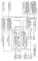
- a unit FPAU when a unit FPAU reads data from a selected PMEM, a programmably selectable delay of either four or six instruction cycles is interposed between the transfer of the memory address over the crossbar address bus to PMEM, and the subsequent transfer of PMEM output data over the crossbar data bus to the FPAU.
- the crossbar steering vector (the 3LSB of the address), which is provided by the FPAU along with the memory address (and parity), is initially sent through uni-directional crossbar switch 110 to select the proper PMEM module.
- the steering vector is also saved in a programmable length shift register 112 which provides the variable pipeline delay for subsequent steering of the memory output data to the requesting FPAU after the selected number of instruction cycle delays (either four or six) have elapsed. If a six cycle delay is selected, then two additional delay cycles must be added by programmable length shift register 114 to the data returning from memory (four delays are inherent, as set forth in Fig. 12 and the discussion which follows). Both data written into memory and read from memory passes across bidirectional bus 116 and through bidirectional crossbar switch 118.
- FIG. 12 A timing diagram illustrating the activity on the crossbar address bus and data bus for a memory read sequence of five samples with a four-cycle delay is presented in Fig. 12.
- Interlaced patterns of memory reads and writes may be achieved as long as a processor does not attempt to write to a memory four cycles after a memory read has been initiated. To do so would cause a data bus clash since the processor cannot simultaneously transmit and receive data on crossbar data bus during the same instruction cycle. Similarly, if a six-cycle delay is selected, then no memory write cycle can be performed six cycles after a memory read has been initiated.
- the memory access sequence consists of a repetitive pattern of two memory read cycles followed by a memory write cycle ; this three cycle memory access pattern is repeated for every vector element.
- a timing diagram illustrating crossbar bus activity for this memory access pattern with a four-cycle delay is shown in Fig. 13, where the i and j notation represents the flow of data through the crossbar switch during the i th read cycle and j th write cycle, respectively.
- Fig. 13 with a four-cycle delay, extra instruction cycles are required to prevent bus clash.
- a six-cycle delay select feature illustrated in Fig. 14, the execution time of this algorithm is decreased by 25%.
Landscapes
- Engineering & Computer Science (AREA)
- Theoretical Computer Science (AREA)
- Physics & Mathematics (AREA)
- Software Systems (AREA)
- Computer Hardware Design (AREA)
- General Engineering & Computer Science (AREA)
- General Physics & Mathematics (AREA)
- Mathematical Physics (AREA)
- Multi Processors (AREA)
- Complex Calculations (AREA)
- Advance Control (AREA)
- Use Of Switch Circuits For Exchanges And Methods Of Control Of Multiplex Exchanges (AREA)
Applications Claiming Priority (2)
| Application Number | Priority Date | Filing Date | Title |
|---|---|---|---|
| US11756487A | 1987-11-06 | 1987-11-06 | |
| US117564 | 1987-11-06 |
Publications (2)
| Publication Number | Publication Date |
|---|---|
| EP0315550A2 true EP0315550A2 (de) | 1989-05-10 |
| EP0315550A3 EP0315550A3 (de) | 1989-10-25 |
Family
ID=22373592
Family Applications (1)
| Application Number | Title | Priority Date | Filing Date |
|---|---|---|---|
| EP88402787A Ceased EP0315550A3 (de) | 1987-11-06 | 1988-11-04 | Hochparallele Rechnerbauweise unter Verwendung eines Koordinatenschalters mit ausgewählter Pipelineverzögerung |
Country Status (2)
| Country | Link |
|---|---|
| EP (1) | EP0315550A3 (de) |
| JP (1) | JPH021086A (de) |
Cited By (4)
| Publication number | Priority date | Publication date | Assignee | Title |
|---|---|---|---|---|
| EP0608663A1 (de) * | 1993-01-25 | 1994-08-03 | BULL HN INFORMATION SYSTEMS ITALIA S.p.A. | Multiprozessorsystem mit gemeinschaftlichem Speicher |
| EP0602916A3 (en) * | 1992-12-14 | 1994-08-10 | Hewlett Packard Co | Cross-bar interconnect apparatus. |
| US5410300A (en) * | 1991-09-06 | 1995-04-25 | International Business Machines Corporation | Distributed crossbar switch architecture |
| US5692139A (en) * | 1988-01-11 | 1997-11-25 | North American Philips Corporation, Signetics Div. | VLIW processing device including improved memory for avoiding collisions without an excessive number of ports |
Families Citing this family (3)
| Publication number | Priority date | Publication date | Assignee | Title |
|---|---|---|---|---|
| KR20100114942A (ko) * | 2002-05-13 | 2010-10-26 | 페어차일드 세미컨덕터 코포레이션 | 직렬화기 및 비직렬화기 기능을 갖는 교차점 스위치 |
| US8966457B2 (en) | 2011-11-15 | 2015-02-24 | Global Supercomputing Corporation | Method and system for converting a single-threaded software program into an application-specific supercomputer |
| US11989591B2 (en) * | 2020-09-30 | 2024-05-21 | Advanced Micro Devices, Inc. | Dynamically configurable overprovisioned microprocessor |
Family Cites Families (7)
| Publication number | Priority date | Publication date | Assignee | Title |
|---|---|---|---|---|
| US3997896A (en) * | 1975-06-30 | 1976-12-14 | Honeywell Information Systems, Inc. | Data processing system providing split bus cycle operation |
| JPS54140438A (en) * | 1978-04-24 | 1979-10-31 | Toshiba Corp | Information processor |
| JPS559217A (en) * | 1978-06-30 | 1980-01-23 | Fujitsu Ltd | Connection system for multiprocessor |
| FR2474199B1 (fr) * | 1980-01-21 | 1986-05-16 | Bull Sa | Dispositif pour superposer les phases successives du transfert des informations entre plusieurs unites d'un systeme de traitement de l'information |
| JPS57209569A (en) * | 1981-06-19 | 1982-12-22 | Fujitsu Ltd | Memory access device in vector processor system |
| JPS58154059A (ja) * | 1982-03-08 | 1983-09-13 | Omron Tateisi Electronics Co | 並列処理システムのメモリアクセス方式 |
| JPS618785A (ja) * | 1984-06-21 | 1986-01-16 | Fujitsu Ltd | 記憶装置アクセス制御方式 |
-
1988
- 1988-11-04 EP EP88402787A patent/EP0315550A3/de not_active Ceased
- 1988-11-07 JP JP28114588A patent/JPH021086A/ja active Pending
Cited By (5)
| Publication number | Priority date | Publication date | Assignee | Title |
|---|---|---|---|---|
| US5692139A (en) * | 1988-01-11 | 1997-11-25 | North American Philips Corporation, Signetics Div. | VLIW processing device including improved memory for avoiding collisions without an excessive number of ports |
| US5410300A (en) * | 1991-09-06 | 1995-04-25 | International Business Machines Corporation | Distributed crossbar switch architecture |
| EP0602916A3 (en) * | 1992-12-14 | 1994-08-10 | Hewlett Packard Co | Cross-bar interconnect apparatus. |
| EP0608663A1 (de) * | 1993-01-25 | 1994-08-03 | BULL HN INFORMATION SYSTEMS ITALIA S.p.A. | Multiprozessorsystem mit gemeinschaftlichem Speicher |
| US5701413A (en) * | 1993-01-25 | 1997-12-23 | Bull Hn Information Systems Italia S.P.A. | Multi-processor system with shared memory |
Also Published As
| Publication number | Publication date |
|---|---|
| JPH021086A (ja) | 1990-01-05 |
| EP0315550A3 (de) | 1989-10-25 |
Similar Documents
| Publication | Publication Date | Title |
|---|---|---|
| US5081575A (en) | Highly parallel computer architecture employing crossbar switch with selectable pipeline delay | |
| US5428803A (en) | Method and apparatus for a unified parallel processing architecture | |
| US5815723A (en) | Picket autonomy on a SIMD machine | |
| KR970001899B1 (ko) | 메모리연결형 파면어레이 프로세서 | |
| Rettberg et al. | Contention is no obstacle to shared-memory multiprocessing | |
| KR0147060B1 (ko) | 데이타 프로세서 시스템과 이를 이용한 비디오 프로세서 시스템 | |
| EP0085520B1 (de) | Architektur von Datenfeldprozessoren mit modularen Elementarprozessoren | |
| US5809292A (en) | Floating point for simid array machine | |
| US5903771A (en) | Scalable multi-processor architecture for SIMD and MIMD operations | |
| US4942517A (en) | Enhanced input/output architecture for toroidally-connected distributed-memory parallel computers | |
| US5805915A (en) | SIMIMD array processing system | |
| US4773038A (en) | Method of simulating additional processors in a SIMD parallel processor array | |
| US5247613A (en) | Massively parallel processor including transpose arrangement for serially transmitting bits of data words stored in parallel | |
| US5148547A (en) | Method and apparatus for interfacing bit-serial parallel processors to a coprocessor | |
| US5630162A (en) | Array processor dotted communication network based on H-DOTs | |
| GB2122781A (en) | Multimicroprocessor systems | |
| KR100280854B1 (ko) | 데이타 처리 장치 및 데이타 처리 방법 | |
| JPH04267466A (ja) | 連想並列処理システム | |
| EP0532700A4 (en) | Multi-dimensional processor system and processor array with massively parallel input/output | |
| EP0263500B1 (de) | Vektordatenverarbeitungssystem mit einer E/A-Steuerung für jeden Vektordatenprozessor und einer anderen E/A-Steuerung für mindestens einen anderen Vektordatenprozessor | |
| EP0315550A2 (de) | Hochparallele Rechnerbauweise unter Verwendung eines Koordinatenschalters mit ausgewählter Pipelineverzögerung | |
| US20040078093A1 (en) | Array-type processor | |
| EP1792258B1 (de) | Verbindungen in simd-prozessorarchitekturen | |
| US20040250047A1 (en) | Method and apparatus for a shift register based interconnection for a massively parallel processor array | |
| Schimmler et al. | The instruction systolic array—Implementation of a low-cost parallel architecture as add-on board for personal computers |
Legal Events
| Date | Code | Title | Description |
|---|---|---|---|
| PUAI | Public reference made under article 153(3) epc to a published international application that has entered the european phase |
Free format text: ORIGINAL CODE: 0009012 |
|
| AK | Designated contracting states |
Kind code of ref document: A2 Designated state(s): AT BE CH DE ES FR GB GR IT LI LU NL SE |
|
| 17P | Request for examination filed |
Effective date: 19890627 |
|
| PUAL | Search report despatched |
Free format text: ORIGINAL CODE: 0009013 |
|
| AK | Designated contracting states |
Kind code of ref document: A3 Designated state(s): AT BE CH DE ES FR GB GR IT LI LU NL SE |
|
| 17Q | First examination report despatched |
Effective date: 19900727 |
|
| STAA | Information on the status of an ep patent application or granted ep patent |
Free format text: STATUS: THE APPLICATION HAS BEEN REFUSED |
|
| 18R | Application refused |
Effective date: 19910824 |