EP0316059A2 - Mikrowellen-Impulsgenerator - Google Patents
Mikrowellen-Impulsgenerator Download PDFInfo
- Publication number
- EP0316059A2 EP0316059A2 EP88307520A EP88307520A EP0316059A2 EP 0316059 A2 EP0316059 A2 EP 0316059A2 EP 88307520 A EP88307520 A EP 88307520A EP 88307520 A EP88307520 A EP 88307520A EP 0316059 A2 EP0316059 A2 EP 0316059A2
- Authority
- EP
- European Patent Office
- Prior art keywords
- pulses
- signal generator
- signal
- providing
- coupled
- Prior art date
- Legal status (The legal status is an assumption and is not a legal conclusion. Google has not performed a legal analysis and makes no representation as to the accuracy of the status listed.)
- Withdrawn
Links
- 230000003287 optical effect Effects 0.000 claims abstract description 21
- 239000000758 substrate Substances 0.000 claims abstract description 9
- 230000005540 biological transmission Effects 0.000 claims abstract description 8
- GPXJNWSHGFTCBW-UHFFFAOYSA-N Indium phosphide Chemical compound [In]#P GPXJNWSHGFTCBW-UHFFFAOYSA-N 0.000 claims description 4
- JBRZTFJDHDCESZ-UHFFFAOYSA-N AsGa Chemical compound [As]#[Ga] JBRZTFJDHDCESZ-UHFFFAOYSA-N 0.000 claims description 2
- 229910001218 Gallium arsenide Inorganic materials 0.000 claims description 2
- 229910003460 diamond Inorganic materials 0.000 claims description 2
- 239000010432 diamond Substances 0.000 claims description 2
- 238000005286 illumination Methods 0.000 claims description 2
- 229910052710 silicon Inorganic materials 0.000 claims description 2
- 239000010703 silicon Substances 0.000 claims description 2
- 230000008878 coupling Effects 0.000 abstract description 3
- 238000010168 coupling process Methods 0.000 abstract description 3
- 238000005859 coupling reaction Methods 0.000 abstract description 3
- 238000000926 separation method Methods 0.000 abstract 1
- 239000007787 solid Substances 0.000 description 6
- 239000003990 capacitor Substances 0.000 description 5
- 238000011084 recovery Methods 0.000 description 5
- 230000001747 exhibiting effect Effects 0.000 description 3
- XEEYBQQBJWHFJM-UHFFFAOYSA-N Iron Chemical compound [Fe] XEEYBQQBJWHFJM-UHFFFAOYSA-N 0.000 description 2
- 238000000034 method Methods 0.000 description 2
- 235000014676 Phragmites communis Nutrition 0.000 description 1
- 238000013459 approach Methods 0.000 description 1
- 230000015556 catabolic process Effects 0.000 description 1
- 239000004020 conductor Substances 0.000 description 1
- 230000006866 deterioration Effects 0.000 description 1
- 238000010586 diagram Methods 0.000 description 1
- 238000007599 discharging Methods 0.000 description 1
- 238000010438 heat treatment Methods 0.000 description 1
- 229910052742 iron Inorganic materials 0.000 description 1
- QSHDDOUJBYECFT-UHFFFAOYSA-N mercury Chemical compound [Hg] QSHDDOUJBYECFT-UHFFFAOYSA-N 0.000 description 1
- 229910052753 mercury Inorganic materials 0.000 description 1
Images
Classifications
-
- H—ELECTRICITY
- H03—ELECTRONIC CIRCUITRY
- H03K—PULSE TECHNIQUE
- H03K17/00—Electronic switching or gating, i.e. not by contact-making and –breaking
- H03K17/51—Electronic switching or gating, i.e. not by contact-making and –breaking characterised by the components used
- H03K17/78—Electronic switching or gating, i.e. not by contact-making and –breaking characterised by the components used using opto-electronic devices, i.e. light-emitting and photoelectric devices electrically- or optically-coupled
Definitions
- the subject of the invention pertains to the field of short pulse generators and more particularly to short pulse generators capable of providing bursts of microwave energy without the utilization of an active microwave oscillator.
- Short baseband pulses of sub-nanosecond duration have bandwidths that extend from d. c. well into the microwave region.
- Hertzian spark gap generators. These devices can supply pulses with amplitudes in the order of one thousand volts and rise times in the order of one hundred picoseconds at repetition frequencies above two hundred hertz. Hertzian generators, however, have a lifetime limited by the width of the spark gap which determines the width of the generated pulse.
- Nano-second pulses with rise times in the order of twenty-five picoseconds are achievable with tunnel diodes. These generators, however, are low amplitude devices achieving levels only in the order of 0.5 volts. Short pulses with amplitudes as high as one thousand volts have been generated with a series stack of avalanche transistors. The rise and fall times of these generators is in the order of six nanoseconds, which for many applications is too slow. A significant improvement in the pulse rise time has been achieved with the combination of avalanche transistors and step-recovery diodes. These devices exhibit rise times in the order of one hundred picoseconds but provide peak amplitudes only in the order of twenty five volts.
- a short pulse generator in the prior art capable of providing pulse widths of four hundred picoseconds at an amplitude of one hundred volts utilizes a step recovery diode fired by the discharge of three capacitors.
- the three capacitors are charged in parallel and then, by means of fast switching avalanche transistors, are connected in series for discharge to obtain a voltage that is substantially equal to the sum of the capacitor voltages when charged.
- the series coupled capacitors are then coupled via an output avalanche transistor to a differentiator causing a doublet pulse to be coupled to the step-recovery diode.
- This doublet pulse triggers the step-recovery diode stack to provide a fast rise time, high voltage pulse of sub-nanosecond duration. While this device provides high voltage sub-nanosecond pulses,the operation of charging and discharging the capacitors to trigger the avalanche transistors requires complex circuitry and components of very narrow tolerances to achieve the desired pulse widths.
- a signal generator capable of providing high energy, short pulse electrical signals in accordance with the principles of the present invention may comprise an electrical signal source coupled to a photon-excited solid state switch positioned to receive a short burst of optical energy. Upon the reception of the optical energy the photon-excited solid state switch is activated and passes the signals from the electrical signal source to an output terminal. The photon-excited solid state switch remains activated for the duration of the optical signal and returns to its original state when the optical signal is removed. These photon-excited solid state switches are sensitive to the amplitude of the optical signals, thereby providing electrical signals of an amplitude variation and time duration equal to that of the optical signal.
- the short pulse electrical signals at the output of the photon-excited solid state switch may be coupled to a bandpass filter to provide signals at desired center frequency and bandwidth at the output terminals of the bandpass filter.
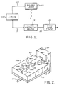
- a timing circuit 11 generates a pulse which is coupled via line 13 to a laser 15 causing the laser to emit photons for the duration of the pulse.
- the timing circuit 11 Prior to the generation of the pulse, the timing circuit 11 provides a signal of desired amplitude via line 17 to a photo-conductive switch positioned between the line 17 and an output line 20.
- the photo-conductive switch 19 may be of the suitably doped silicon, gallium arsenide, diamond or indium phosphide type and presents, in the absence of photon illumination, a high impedance between the lines 17 and 20 that approaches an open circuit.
- timing circuit 11 When photons of sufficient energy illuminate the switch the electrons in the photo-conductive material are excited into free cnduction energy bands, thereby providing a conduction path between the lines 17 and 20 causing the voltage from timing circuit 11 to be coupled through the switch 19 to the input terminals of bandpass filter 21.
- the photo conductive switch 19 reacts with sufficient rapidity to follow the photon pulse emitted by the laser 15. Sometime after the coupling of the pulse to the line 13, timing circuit 11 terminates the voltage coupled to the photo-conductive switch, thus reducing ohmic heating of the switch substrate and thereby preventing thermal runaway.
- the photo-conductive switch 19 is constructed to match the impedance of the termination at the output port of the switch.
- the output port of the photo-conductive switch 19 is constructed to provide an impedance matched to the transmission line type utilized by the bandpass filter 21.
- the switch comprises a microstrip transmission line formed by metallic strips 27a and 27b positioned on an iron doped indium phosphide substrate 29 which is backed by a conducting ground plane 31.
- a gap 33 between the metallic strips 27a and 27b is located to receive protons from the laser source 15 not shown in this figure.
- Electrodes 35a and 35b extend from the metallic the strip 27a and from the ground plane 31,respectively, for coupling to the voltage source in the timing circuit 11.
- This signal is via strip 27b and matching section 37,to the filter 21, not shown in Figure 2.
- the width of the gap 33 is an important variable in the design of the pulse generator.
- High energy pulses require a high voltage across the gap and the gap width must be sufficient to prevent dielectric breakdown (arcing) across the gap. It should be recognized, however, that the optical energy required to affect photo induced conductivity is directly proportional to the gap width. Thus it is apparent that the transmission of high-peak energy pulses require a high voltage signal source and a relatively high energy optical source.
- the shape and length of the pulse at the output port of the filter is a function of a number of factors, including the shape of the optical pulse provided by the laser and the frequency response of the filter.
- an optical pulse exhibiting a Gaussian envelope and a filter with a rectangular frequency response of sufficient bandwidth provides signals within a frequency band having an amplitude distribution with frequency that is also Gaussian.
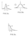
- an optical pulse 37 with a Gaussian amplitude function of time is shown.
- This function has a Fourier transform which provides signals with a Gaussian amplitude distribution 39 in the frequency domain, as shown in Figure 3b. If the signal coupled across terminals 35a and 35b is a D. C. signal, the frequency f0 is 0 and in a one-sided Fourier transform results, exhibiting a Gaussian amplitude distribution with frequency extending from D. C., as indicated by the amplitude distribution 41 in Figure 3c.
- a filter with a square frequency response transmits signals coupled thereto, within its frequency band, without varying the amplitude distribution of the coupled signals.
- a truncated band of frequencies coupled to the input terminal of the filter, exhibiting a Gaussian amplitude distribution over a frequency range only within the passband of the filter will emerge therefrom with the same truncated Gaussian distribution.
- the bandwidth of the filter is between f a and f b as shown in Figure 3c the signals emerging therefrom will have and amplitude distribution over that portion of the Gaussian envelope within the frequency band.
- the pulse length T of the Gaussian optical pulse is chosen to maximize the integrated energy within the filter passband.
Landscapes
- Semiconductor Lasers (AREA)
- Electronic Switches (AREA)
Applications Claiming Priority (2)
| Application Number | Priority Date | Filing Date | Title |
|---|---|---|---|
| US118812 | 1987-11-09 | ||
| US07/118,812 US4822991A (en) | 1987-11-09 | 1987-11-09 | Optically switched microwave pulse generator |
Publications (2)
| Publication Number | Publication Date |
|---|---|
| EP0316059A2 true EP0316059A2 (de) | 1989-05-17 |
| EP0316059A3 EP0316059A3 (de) | 1990-05-16 |
Family
ID=22380894
Family Applications (1)
| Application Number | Title | Priority Date | Filing Date |
|---|---|---|---|
| EP88307520A Withdrawn EP0316059A3 (de) | 1987-11-09 | 1988-08-12 | Mikrowellen-Impulsgenerator |
Country Status (3)
| Country | Link |
|---|---|
| US (1) | US4822991A (de) |
| EP (1) | EP0316059A3 (de) |
| DK (1) | DK625388A (de) |
Cited By (1)
| Publication number | Priority date | Publication date | Assignee | Title |
|---|---|---|---|---|
| EP0517441A1 (de) * | 1991-06-06 | 1992-12-09 | AT&T Corp. | Dynamische optische Logik |
Families Citing this family (14)
| Publication number | Priority date | Publication date | Assignee | Title |
|---|---|---|---|---|
| US4831248A (en) * | 1987-08-07 | 1989-05-16 | Center For Innovative Technology | Electron beam controlled bulk semiconductor switch with cathodoluminescent electron activation |
| US5003168A (en) * | 1988-12-22 | 1991-03-26 | Alfano Robert R | Trigger circuit for a streak camera sweep drive circuit |
| US5153442A (en) * | 1989-06-12 | 1992-10-06 | The United States Of America As Represented By The Secretary Of The Army | High power, solid state RF pulse generators |
| US5146075A (en) * | 1991-04-08 | 1992-09-08 | The United States Of America As Represented By The Secretary Of The Army | Ligh activated high power integrated pulser |
| US5177486A (en) * | 1991-11-25 | 1993-01-05 | The United States Of America As Represented By The Secretary Of The Army | Optically activated hybrid pulser with patterned radiating element |
| US5155352A (en) * | 1991-11-25 | 1992-10-13 | The United States Of America As Represented By The Secretary Of The Army | Optically activated sub-nanosecond hybrid pulser |
| JPH09148895A (ja) * | 1995-11-20 | 1997-06-06 | Advantest Corp | 短電気パルス発生装置 |
| DE19948384B4 (de) * | 1999-10-07 | 2008-04-10 | Rohde & Schwarz Gmbh & Co. Kg | Anordnung zum Bestimmen der komplexen Übertragungsfunktion eines Messgerätes |
| US8563957B2 (en) * | 2009-05-07 | 2013-10-22 | Lawrence Livermore National Security, Llc. | Photoconductive switch package |
| KR101746799B1 (ko) | 2015-11-04 | 2017-06-14 | 주식회사 쏠리드 | 분산 안테나 시스템 |
| US11804839B1 (en) * | 2020-01-28 | 2023-10-31 | Government Of The United States As Represented By The Secretary Of The Air Force | Integrated trigger photoconductive semiconductor switch |
| US20220165905A1 (en) * | 2020-11-20 | 2022-05-26 | The Board Of Trustees Of The Leland Stanford Junior University | Devices and methods involving diamond-based photoconductive structures |
| CN113540942B (zh) * | 2021-05-31 | 2023-05-09 | 北京无线电测量研究所 | 一种快前沿微波脉冲产生装置及方法 |
| CN114545221B (zh) * | 2022-02-25 | 2025-02-18 | 西安交通大学 | 一种气体开关绝缘恢复特性测试实验装置 |
Family Cites Families (7)
| Publication number | Priority date | Publication date | Assignee | Title |
|---|---|---|---|---|
| US4135099A (en) * | 1977-09-15 | 1979-01-16 | Westinghouse Electric Corp. | High energy, short duration pulse system |
| US4218618A (en) * | 1979-02-21 | 1980-08-19 | The University Of Rochester | Apparatus for switching high voltage pulses with picosecond accuracy |
| US4396833A (en) * | 1981-01-22 | 1983-08-02 | Harris Corporation | Optomicrowave integrated circuit |
| US4691111A (en) * | 1984-04-05 | 1987-09-01 | The United States Of America As Represented By The Secretary Of The Army | Multiple gap optically activated switch |
| US4577114A (en) * | 1984-05-17 | 1986-03-18 | The United States Of America As Represented By The Secretary Of The Army | High power optical switch for microsecond switching |
| US4695733A (en) * | 1984-10-17 | 1987-09-22 | Philip Pesavento | Photoconductive power switch |
| US4749850A (en) * | 1987-04-27 | 1988-06-07 | American Telephone And Telegraph Company | High speed quantum well optical detector |
-
1987
- 1987-11-09 US US07/118,812 patent/US4822991A/en not_active Expired - Lifetime
-
1988
- 1988-08-12 EP EP88307520A patent/EP0316059A3/de not_active Withdrawn
- 1988-11-09 DK DK625388A patent/DK625388A/da not_active Application Discontinuation
Non-Patent Citations (2)
| Title |
|---|
| LASER FOCUS, vol. 18, no. 4, April 1982, pages 89-93; AUSTON et al.: "Picosecond optical electronics for high-speed instrumentation" * |
| MICRONOTES, vol. 5, no. 1, June 1967, Microwave Associates, Burlington, Massachusetts, US * |
Cited By (1)
| Publication number | Priority date | Publication date | Assignee | Title |
|---|---|---|---|---|
| EP0517441A1 (de) * | 1991-06-06 | 1992-12-09 | AT&T Corp. | Dynamische optische Logik |
Also Published As
| Publication number | Publication date |
|---|---|
| DK625388D0 (da) | 1988-11-09 |
| EP0316059A3 (de) | 1990-05-16 |
| US4822991A (en) | 1989-04-18 |
| DK625388A (da) | 1989-05-10 |
Similar Documents
| Publication | Publication Date | Title |
|---|---|---|
| US4822991A (en) | Optically switched microwave pulse generator | |
| EP0094765B1 (de) | Kurzimpulsgenerator | |
| US3917943A (en) | Picosecond semiconductor electronic switch controlled by optical means | |
| US5227621A (en) | Ultra-wideband high power photon triggered frequency independent radiator | |
| US3748528A (en) | Microwave generator | |
| US5155352A (en) | Optically activated sub-nanosecond hybrid pulser | |
| GB2043341A (en) | Apparatus for switching high voltage pulses with picosecond accuracy | |
| US5351063A (en) | Ultra-wideband high power photon triggered frequency independent radiator with equiangular spiral antenna | |
| US3612899A (en) | Generator for short-duration high-frequency pulse signals | |
| US4127784A (en) | Light activated solid state microwave generators | |
| US4691111A (en) | Multiple gap optically activated switch | |
| US5017793A (en) | Optically driven RF generator | |
| US5773817A (en) | Ultrafast, high voltage pulser using circumferentially illuminated, laser-switched radial transmission line | |
| US3881120A (en) | Pulse generating circuit | |
| US3629731A (en) | Sampling system | |
| US4053854A (en) | Q switching microwave oscillator | |
| US5283584A (en) | High power photon triggered ultra-wideband RF radiator with opposite apertures | |
| US4115708A (en) | Fast-switching pulse modulator | |
| US4633286A (en) | Multiple gap optically activated switch | |
| Patel et al. | Microstrip plasma limiter | |
| US3241076A (en) | Signal sampling circuit including a signal conductor disposed in the electromagneticfield of a shorted transmission line | |
| Hahn et al. | Nanosecond, kilovolt pulse generators | |
| US3366805A (en) | Semiconductor diode microwave pulse generator | |
| US3521197A (en) | High frequency power limiter device for a waveguide | |
| US5262657A (en) | Optically activated wafer-scale pulser with AlGaAs epitaxial layer |
Legal Events
| Date | Code | Title | Description |
|---|---|---|---|
| PUAI | Public reference made under article 153(3) epc to a published international application that has entered the european phase |
Free format text: ORIGINAL CODE: 0009012 |
|
| AK | Designated contracting states |
Kind code of ref document: A2 Designated state(s): BE DE ES FR GB NL SE |
|
| PUAL | Search report despatched |
Free format text: ORIGINAL CODE: 0009013 |
|
| AK | Designated contracting states |
Kind code of ref document: A3 Designated state(s): BE DE ES FR GB NL SE |
|
| 17P | Request for examination filed |
Effective date: 19901114 |
|
| STAA | Information on the status of an ep patent application or granted ep patent |
Free format text: STATUS: THE APPLICATION IS DEEMED TO BE WITHDRAWN |
|
| 18D | Application deemed to be withdrawn |
Effective date: 19920303 |