EP0316356B1 - Verbesserung an oder hinsichtlich messungen - Google Patents
Verbesserung an oder hinsichtlich messungen Download PDFInfo
- Publication number
- EP0316356B1 EP0316356B1 EP87905376A EP87905376A EP0316356B1 EP 0316356 B1 EP0316356 B1 EP 0316356B1 EP 87905376 A EP87905376 A EP 87905376A EP 87905376 A EP87905376 A EP 87905376A EP 0316356 B1 EP0316356 B1 EP 0316356B1
- Authority
- EP
- European Patent Office
- Prior art keywords
- pattern
- intensity
- signals
- displacement
- detectors
- Prior art date
- Legal status (The legal status is an assumption and is not a legal conclusion. Google has not performed a legal analysis and makes no representation as to the accuracy of the status listed.)
- Expired
Links
- 238000006073 displacement reaction Methods 0.000 claims abstract description 35
- 238000000034 method Methods 0.000 claims abstract description 14
- 230000005855 radiation Effects 0.000 claims description 14
- 230000004044 response Effects 0.000 claims description 10
- 230000008859 change Effects 0.000 claims description 7
- 230000005670 electromagnetic radiation Effects 0.000 claims description 3
- 238000005259 measurement Methods 0.000 claims description 2
- 238000009877 rendering Methods 0.000 claims 1
- 238000009795 derivation Methods 0.000 abstract description 3
- 230000014509 gene expression Effects 0.000 abstract 1
- 230000003287 optical effect Effects 0.000 description 16
- 239000000523 sample Substances 0.000 description 12
- IRLPACMLTUPBCL-KQYNXXCUSA-N 5'-adenylyl sulfate Chemical compound C1=NC=2C(N)=NC=NC=2N1[C@@H]1O[C@H](COP(O)(=O)OS(O)(=O)=O)[C@@H](O)[C@H]1O IRLPACMLTUPBCL-KQYNXXCUSA-N 0.000 description 6
- 230000008901 benefit Effects 0.000 description 4
- 238000005305 interferometry Methods 0.000 description 4
- 238000004364 calculation method Methods 0.000 description 3
- 238000005286 illumination Methods 0.000 description 3
- 230000010354 integration Effects 0.000 description 3
- 230000009021 linear effect Effects 0.000 description 3
- 230000010363 phase shift Effects 0.000 description 3
- 230000010287 polarization Effects 0.000 description 3
- 238000012545 processing Methods 0.000 description 3
- 230000007704 transition Effects 0.000 description 3
- 238000013459 approach Methods 0.000 description 2
- 230000002238 attenuated effect Effects 0.000 description 2
- 238000006243 chemical reaction Methods 0.000 description 2
- 230000001934 delay Effects 0.000 description 2
- 230000003111 delayed effect Effects 0.000 description 2
- 238000010586 diagram Methods 0.000 description 2
- 230000000694 effects Effects 0.000 description 2
- 238000004519 manufacturing process Methods 0.000 description 2
- 230000007935 neutral effect Effects 0.000 description 2
- 238000009825 accumulation Methods 0.000 description 1
- 230000009471 action Effects 0.000 description 1
- 230000002411 adverse Effects 0.000 description 1
- 238000010276 construction Methods 0.000 description 1
- 238000011109 contamination Methods 0.000 description 1
- 230000001419 dependent effect Effects 0.000 description 1
- 229910003460 diamond Inorganic materials 0.000 description 1
- 239000010432 diamond Substances 0.000 description 1
- 239000000428 dust Substances 0.000 description 1
- 230000002452 interceptive effect Effects 0.000 description 1
- 239000002184 metal Substances 0.000 description 1
- 238000003801 milling Methods 0.000 description 1
- 238000012544 monitoring process Methods 0.000 description 1
- 230000009022 nonlinear effect Effects 0.000 description 1
- 230000001151 other effect Effects 0.000 description 1
- 230000001360 synchronised effect Effects 0.000 description 1
- 230000002123 temporal effect Effects 0.000 description 1
Images



Classifications
-
- G—PHYSICS
- G01—MEASURING; TESTING
- G01B—MEASURING LENGTH, THICKNESS OR SIMILAR LINEAR DIMENSIONS; MEASURING ANGLES; MEASURING AREAS; MEASURING IRREGULARITIES OF SURFACES OR CONTOURS
- G01B9/00—Measuring instruments characterised by the use of optical techniques
- G01B9/02—Interferometers
- G01B9/02055—Reduction or prevention of errors; Testing; Calibration
- G01B9/02075—Reduction or prevention of errors; Testing; Calibration of particular errors
- G01B9/02078—Caused by ambiguity
- G01B9/02079—Quadrature detection, i.e. detecting relatively phase-shifted signals
- G01B9/02081—Quadrature detection, i.e. detecting relatively phase-shifted signals simultaneous quadrature detection, e.g. by spatial phase shifting
-
- G—PHYSICS
- G01—MEASURING; TESTING
- G01B—MEASURING LENGTH, THICKNESS OR SIMILAR LINEAR DIMENSIONS; MEASURING ANGLES; MEASURING AREAS; MEASURING IRREGULARITIES OF SURFACES OR CONTOURS
- G01B9/00—Measuring instruments characterised by the use of optical techniques
- G01B9/02—Interferometers
- G01B9/02083—Interferometers characterised by particular signal processing and presentation
Definitions
- This invention relates to measuring, and more particularly, but not exclusively, it relates to interferometers.
- phase term, 8 0 is related to the path length difference, ⁇ L, between the two light beam paths, i.e., the path of fixed length (L R ) and the path of variable length (L T ).
- L R path of fixed length
- L T path of variable length
- TPSI Temporal Phase Shift Interferometry
- FP Four Photodetector
- the FP technique uses four photodetectors disposed in a linear array extending perpendicularly to the fringe pattern.
- the centers of the individual detectors are spaced apart distance d with d being equal to i.e., one-fourth the fringe period.
- the intensity detected instantaneously by the four photodetectors is where
- SPSI Spatial Phase Shift Interferometry
- German Patent Specification 21 59 134 describes means for creating a first beam of monochromatic electromagnetic radiation and beam splitting means disposed in the first beam for creating second and third beams.
- second directing means for directing the third beam along a second path of variable length to be incident on the sensing means whereat it interferes with the second beam and creates a straight line interference pattern.
- each of the detectors is adapted to provide a signal indicative of the intensity of radiation incident on it.
- the signals from the aforesaid four detectors include a term varying sinusoidally as the pattern moves across the detectors responsive to a variation in length of the second path.
- the sinusoidally varying term is the product of a component indicative of the sensed amplitude of the sinusoidal variation of the radiation intensity and a sinusoidal factor including a spactial variable and the path length difference.
- the outputs from detectors are manipulated so that the fringe irradiance values B x , are made equal.
- the phase can be defined using only three detectors disposed on centers at as follows:
- To determine the displacement associated with the phase calculated requires deriving the difference between the currently determined phase and the immediately previously determined phase. The difference is then multiplied by the conversion factor and the result is accumulated.
- An interferometric instrument embodying the present invention will now be described which is intended for measuring displacement of a part during a manufacturing operation.
- the interferometer 10 includes a source of electromagnetic radiation of a single, constant wavelength, in the present embodiment a wavelength-stabilized laser diode 12.
- the actual wavelength of the radiation emitted by the laser diode 12 is not important to the invention but, in the present case wherein the laser diode is a Hitachi Model 8312, the wavelength of the radiation it produces is 0.824 1-1.
- the beam of radiation emitted by the laser diode is passed through an expander collimater 14 which directs an expanded and collimated beam 15 towards a splitter 16 by which the beam 15 is split into second and third means 20 and 22, respectively.
- a polarizing plate 18 which polarizes the radiation beam at 45° so that the intensities of the transmitted and reflected beams 20 and 22, respectively, are equal.
- a neutral density filter 13 between the collimator 14 and the polarizing plate 18 there is a neutral density filter 13 to strongly attenuate any return beam to prevent any optical feedback to the laser diode 12.
- the reflected beam 22 passes through a quarter-wave plate 24 and is then incident on a stationary reflector 26 which reflects the beam back along its path through the quarter-wave plate 24 to the beam splitter 16.
- Stationary mirror 26 is slightly tilted from a plane normal to the beam so that a pattern of interference fringes is generated in the interferometer 10.
- the beam is transmitted by the beam splitter 16 with minimal reflection towards the plate 18.
- the beam reflected by the reflector 26 passes on from the splitter 16, as beam 29, through a polarizing plate 28 and is incident upon a sensor array 30.
- the beam 20, which had been transmitted by the splitter 16 passes through a quarter-wave plate 32 and is incident on a reflector 34 which, in the present embodiment, is in the form of a catseye retroreflector.
- the reflector 34 reflects the beam back upon itself through the quarter-wave plate 32 to the splitter 16 wherein, by virtue of its polarization imposed by the plate 32, it is substantially entirely reflected, as beam 36, towards the sensor array 30 upon which it is incident with only minimal energy being transmitted. This transmitted energy is attenuated by the neutral density filter 13.
- the reflector 26 is stationary but the reflector 34 is associated with a probe 38 in contact with the surface 40 of a part 42 being operated upon and liable to displacement, during a manufacturing operation.
- the polarizing plate 28 imposes the same polarization on the two beams 29 and 36 so that they inherently have the capability of interfering.
- the paths 15, 22, 29 and 15, 20, 36 have path lengths which may be termed L R and L T , respectively.
- L R is of fixed length and LT is of variable length.
- the difference in path lengths is AL. Because there is a difference in path length the two beams interfere and create a straight line fringe pattern, a portion of which is represented in Fig. 2.
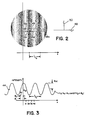
- Fig. 2 represents a portion of the fringe pattern which is of sinusoidal intensity, as represented by the sine curve 44 in Fig. 3.
- the period of the curve 44, in the x direction, is shown in Figs. 2 and 3 as (f o being the spatial frequency of the fringes).
- Fig. 2 also shows the sensor array 30 which includes a plurality of detectors 46a, 46b, 46c, 46d ... 46n.
- the detectors are shown as contiguous for the sake of convenience. However, they are more accurately represented in Figs. 4, 5 and 6, wherein they are small and discrete but can still be formed in an array.
- the array 30 is in a plane perpendicular to the beams 29 and 36 and the individual detectors 46 are disposed along a line 48 perpendicular to lines 50 of uniform intensity in the fringe pattern.
- the detectors 46 have their centers spaced distance d apart.
- Dimension 'd' is equal to a quarter of a fringe period, i.e.
- Fig. 3 is a sinusoidal curve representing the perfect case intensity of illumination in the fringe pattern of Fig. 2.
- the curve might be that generated by the signal from a single small detector scanned through the fringe pattern as produced by two uniform beams.
- the purpose of Fig. 3 is to show the relationship of various terms and parameters.
- Adjacent detectors have different intensities of light incident on them by virtue of the sinusoidal form of the fringe pattern. If no other effects were involved, these intensities would be given by
- Fig. 4 shows a curve for intensity against distance for a single ideal fringe whose spatial period is exactly matched to the length of the array of four detectors.
- the detectors are represented in Fig. 4 and it will be seen that they are relatively small and spaced rather than contiguous.
- Fig. 5 represents a possible intensity profile 51 which would be present over the detectors if the two beams 29 and 36 were present without interference.
- the lack of uniformity of intensity may be due to dust, hot spots, internal reflections, etc.
- the line 52 at intensity of 1 represents an ideal intensity.
- the plot is of the actual intensity and it can be seen that there is an optical gain (OG) in the intensity of the four detectors of 0.9; 1.3; 1.0; and 1.03, respectively.
- OG optical gain
- Fig. 10 represents a voltage against phase plot for the four detectors with adjustments having been made to give the same AC response, i.e., to make the B x terms equal at 0.3.
- the desired AC response is chosen arbitrarily. It should be noted that simply matching the gain of each of the detectors will not provide the results shown, since the detector gain is only one source of gain error. With these adjustments:
- the detector outputs (I 1 , I 2 , I 3 and I 4 ) are defined solely by the product of the gain terms (optical and electrical) and the intensity incident on the detectors.
- the procedure described to make equal the AC amplitude response of the detectors (B x terms) also resulted in equal DC response (A X terms).
- the result demonstrated is not impossible but highly unlikely.
- the output of a detector is in actuality, derived due to the integrating of the incident light over the aperture of the detector's active area.
- the action of integration is related to ratio of the size of the active area to the center- to-center spacing and has. significant non-linear effects on the detector's response.
- a term P related to the optical power is given by:
- the value of P 1 is directly proportional to P 2 . Therefore, the value of A,'; A 2 '; A 3 ' and A 4 ' can all be determined from either P 1 , or P 2 . Therefore, where
- phase can be determined using only three detectors, e.g., 46a, 46b, 46c as follows:
- To determine the displacement associated with the phase calculated requires deriving the difference between the currently determined phase and the immediately previously determined phase. The difference is then multiplied by the conversion factor and the result is accumulated.
- FIG 11 illustrates schematically the principles of a manner of processing signals from the detectors, in accordance with the present invention.
- Input currents I 1 , I 2 and 1 3 are the outputs of photodiodes 46a, 46b and 46c (see Fig. 12) respectively, with each of the signals taking the following forms:
- variable gain amplifier 74 has as its output voltage 1 3 ', that is A 3 ' -B cos ⁇ 1 .
- This is combined with the output of variable gain amplifier 70 which is I', that is A 1 ' + B cos ⁇ 1 .
- the signals I 1 ' and I 3 ' are combined in adder 78, the output of which is -P or -(A 1 ' + A 3 '), a term which relates to the optical power of the system.
- variable gain amplifier 70 A portion of the output from variable gain amplifier 70 is fed to an adder 80.
- the output P of adder 78 is directed through a multiplier circuit 82 which may take the form of a variable resistor.
- the output of the multiplier circuit 82 is A 1 ', or -K,P, which is added to the I 1 ' signal by the adder 80, resulting in -B cos ⁇ 1 , being sent to the denominator input of an arctangent device 84.
- variable gain amplifier 72 The output of variable gain amplifier 72 is 1 2 ', or A 2 ' + B si ⁇ 1 , which is directed to one of the inputs of adder 86.
- the output signal -P of adder 78 is directed to the input of multiplier circuit 88 which multiplies the input signal -P by a constant -K 2 ' resulting in an output of A 2 '.
- the output of the multiplier circuit 88 is subtracted from 1 2 ' in the adder 86, resulting in the output of the adder 86 being -B sin ⁇ 1 which is then fed to the numerator input of arctangent device 84 which provides an output signal equal to ⁇ 1 . If desired, and not shown in Fig.
- this signal ⁇ 1 may be converted to a digital signal the value of which may be combined with the sign of the -B sin ⁇ 1 , and -B cos ⁇ 1 , terms and compared to those in a look-up table to provide ⁇ 1 , between 0° and 360°.
- Figure 12 is a diagram which illustrates a circuit for the implemtnation of the block diagram in Figure 11.
- the output signals of the detectors 46a, 46b, 46c which, in the present example are photodiodes, provide the input signals to operational amplifiers (OP AMPS) 91, 92, and 93, respectively, which amplify the signals from the respective photodiodes with variable gain such that the AC function, i.e. the "B" term, in the three equations set forth earlier, are made equal.
- the current to laser diode 12 (see Fig. 1) was varied slightly to shift the wavelength while the outputs of OP AMP I 1 ', 1 2 ' and 1 3 ' were monitored.
- the gains of the OP AMPS 91, 92, and 93 were adjusted via variable resistors 300, 301, 302, respectively, to make the peak-to-peak variations of I 1 , I 2 and 1 3 equal.
- the variation in current was selected so that the wavelength change produced at least a 360° phase shift in the interference fringe pattern.
- the outputs of OP AMPS 91 and 93 are added to provide a sum -P which, if the period of the fringes are matched to the spacing of the photodiodes, should result in a function which relates to the optical power of the system. From this power-related function one may derive A 1 ', A 2 ', and A 3 '.
- the combined output signals from OP AMPS 91 and 93 are fed to the input of OP AMP 94 which provides a fixed gain to the signal with its primary function resulting in the sum of I 1 ' and 1 3 ' and the reversa of the arithmetic sign.
- the portion of the circuit within the dotted line 96a performs the same function as multiplexer K 1 shown in Fig. 11.
- K 1 is established during the operation whether the B x terms are being made equal. Once the B x terms have been made equal and with the moving fringe still available, the variable resistor 96 is adjusted for zero average value at the output of OP AMP 98. K 1 need never be changed if A,' changes due solely to optical
- variable resistor 96 and the output of OP AMP 91 are combined and placed on the negative input of OP AMP 98 which provides a fixed gain and is primarily used to sum -k,P and the output of OP AMP 91 to provide -B cos ⁇ 1 , at the output of OP AMP 98.
- a portion of the output signal from OP AMP 94 is directed to the negative input of variable gain OP AMP 102.
- Variable resistor 104 is larger than resistor 106 so that both attenuation and gain may be accomplished by adjusting the gain of OP AMP 102 appropriately using variable resistor 104.
- the output of OP AMP 102 is passed through a voltage divider comprising resistors 108 and 110 which have the same resistance value and result in attenuating the signal by a factor of two resulting in a signal +A 2 '/2.
- the output of OP AMP 92 is brought in on the positive input of OP AMP 112 and subtracted from to form -B sin ⁇ 1 , at output of OP AMP 112.
- power-related term -P is related to the outputs from OP AMPS 91 and 93, A,' and A 3 ' will always be in the form of an attenuation constant. Sicne the power-related term was not obtained using the output from OP AMP 92, A 2 ' either can be an attenuation or can even require a slight gain factor. This is equivalent to shown in Figure 11 and is essentially that portion shown within the dotted lines 120. k 2 ', like k 1 , is also established with the use of a moving fringe. Variable resistor 104 is adjusted for zero average value at the output of OP AMP 112. Once k 2 is defined, it need not be changed if A 2 ' changes due solely to optical power fluctuations.
- k, and k 2 ' are not affected by optical power fluctuation due to the power-related term P, they are susceptible to changes in the background noise. Changes will occur due to misalignment of the interferring beams, contamination of optical surfaces and even improper spatial frequency. Logical combinations of the -B cos ⁇ , -B sin 8 and -P terms can be used to indicate when these conditions exist and the technique is being violated thereby introducing error.
- the outputs of OP AMPS 98 and 112 are used to determine the value of ⁇ 1 .
- Each output signal is fed to a sample and hold device 130 and 132, respectively.
- the sample and hold devices are primarily intended to provide a stable input and prevent any adverse affects that may result from propogation delays or timing shifts that may occur between the different signal paths.
- each of the sample and hold devices 130 and 132 are directed to the negative inputs of respective comparators 134 and 136 each of which use feedback hysteresis to prevent the comparator from oscillating when the signal levels are near zero volts.
- Use of this feedback technique insures a sharp vertical edge whenever the signal level makes a transition at or near a zero voltage level.
- each of the comparators 134 and 136 are fed to a pair of flip flops 138, 140 and 142, 144 respectively which delays the respective signals by one clock period with the final flip flops inverting the signal which had been once inverted by the respective comparators 134 and 136.
- the output of flip flop 140 is fed to the A N+1 bit of the look-up table 160.
- the output of the flip flop 144 is fed to the AN bit of the look-up table 160. It is important to keep in mind that the tangent function repeats itself every 180 degrees. Therefore, in order to keep track of the phase and to have 0-360 degree resolution, the arithmetic signs of "B cos" and "13 sin” terms should be maintained accurately.
- a portion of the output of sample and hold device 130 is fed to the denominator input of an arctangent device 162 (Analog Device Model G39).
- a portion of the output of sample and hold device 132 is fed to the numerator input of the arctangent device 162 which performs the arctangent function between numerator and denominator and outputs the phase ⁇ 1 which provides voltages indicative of -90° to +90°.
- This output signal is fed to an analog to digital converter 166 which in turn sends a digital output signal to the (A N-1 ) - (A o ) address bits in the ROM look-up table 160. It should be recognized that because the arctan function is asymptotic near + or -90°, the higher the resolution of the analog to digital converter 166, the higher will be the resolution of the quantitised phase.
- the look-up table 160 uses the sign of the cosine term which has been delayed one clock period on AN+, input. This signal correlates with the quantitized data appearing at the output of the analog to digital converter 166. The sign of the sine term which was also delayed one clock period is fed in the AN address bit. Shown in Figure 15, is a set of orthogonal axes which form four quadrants. The sign information contained in the sine and cosine inputs will make a determination with respect to the proper quadrant and will provide information concerning the proper angle from zero to 360 degrees and the look-up table will determine the value of the angle ⁇ 1 either in radians or degrees.
- clock 170 Also shown in Figure 13 is the clock 170 and the necessary clocking liens that are needed to provide the required timing.
- phase displacement information is derived from difference of successive phase values. Because 8 1 normally ranges from 0 to 360°, error can result if successive phases were derived from different sinusoid cycles. The error results during the difference operation, since crossing cycles results in repetition of the range of phase values rather than an increment or decrement. To combat the problem, the direction of travel must be sensed using the signs of -B sin 8 and -B cos 6, in a manner known to those skilled in the art, and the phase modified to allow for logical phase differences. To aid understanding, an example will now be given:
- phase inputs assumed to be modified, present at either ⁇ ' 1 n or ⁇ 1 n-1 the difference in phase ⁇ 1 n , is then input to the adder/counter circuit block 202, which adds the lower significant bits of previously accumulated phase differences to the current phase difference.
- the adder/counter counts both up and down to relay both positive and negative displacement from a reference (start) point.
- the adder/counter must be synchronized to the events of the A/D and other functional blocks. Therefore, the clock input is essential to the blocks operation.
- the computer/display interface 204 performs the conversion This block normally operates at much slower rates than blocks 200 and 202 and is usually not implemented until the data is needed. This is important since the faster the phase calculation and accumulation rate, the higher the acceptable rate of travel of the probe. Therefore, the conversion/acquisition cycle does not limit the bandwidth of the system and accurate data is available on request. The eventual accuracy and resolution obtained using this technique are highly dependent on the uniformity of the detector spacing as well as the levels of quantitization used in the analog to digital converter.
- the fringe pattern is created by interference of two beams, one having a path of fixed length and the other having a path for a length variable in proportion to a parameter being measured. Displacement information is derived from changes in the difference in the paths lengths. It is to be understood that the present invention includes also embodiments in which the fringe pattern is not created by interference of two beams but is formed by directing radiation onto or through any sinusoidally varying pattern such as a grating or a modified Ronchi ruling. Thus, in such cases as these, the invention might be expressed as a method of measuring the displacement of an object by analyzing a sinusoidal grating pattern the phase of which changes in direct proportion to displacement of the object.
- the three or more detectors would be disposed to view the pattern on a line perpendicular to the pattern and with the detectors disposed on centers spaced apart by one-fourth the period of the fringe pattern.
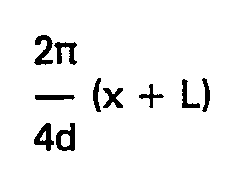
- the intensity sensed by each detector instead of the intensity sensed by each detector being expressed by with the displacement information being gained from changes in AL (the difference in lengths of the paths of the interferometer), the intensity is expresed by wherein L is a parameter which varies with the displacement of the object.
- L is a parameter which varies with the displacement of the object.
- the value of the displacement is derived by accumulating changes in the value of L.
- the derivation again involves the step of adjusting the signals from the detectors so that the B x terms are rendered equal. This technique has the great advantage of allowing the frequency of the grating pattern to be greatly reduced while maintaining and even improving the resolution.
- the interferometric instrument described above is suitable for monitoring the position of the back of the tool in a diamond milling operation for creating a metal surface which is to be used to form an optical surface, amongst many other usages.
Landscapes
- Physics & Mathematics (AREA)
- General Physics & Mathematics (AREA)
- Engineering & Computer Science (AREA)
- Signal Processing (AREA)
- Length Measuring Devices By Optical Means (AREA)
- Instruments For Measurement Of Length By Optical Means (AREA)
- Optical Transform (AREA)
Claims (5)
Priority Applications (1)
| Application Number | Priority Date | Filing Date | Title |
|---|---|---|---|
| AT87905376T ATE54749T1 (de) | 1986-08-04 | 1987-08-03 | Verbesserung an oder hinsichtlich messungen. |
Applications Claiming Priority (2)
| Application Number | Priority Date | Filing Date | Title |
|---|---|---|---|
| US06/893,431 US4776698A (en) | 1986-08-04 | 1986-08-04 | Measuring |
| US893431 | 2001-06-29 |
Publications (2)
| Publication Number | Publication Date |
|---|---|
| EP0316356A1 EP0316356A1 (de) | 1989-05-24 |
| EP0316356B1 true EP0316356B1 (de) | 1990-07-18 |
Family
ID=25401555
Family Applications (1)
| Application Number | Title | Priority Date | Filing Date |
|---|---|---|---|
| EP87905376A Expired EP0316356B1 (de) | 1986-08-04 | 1987-08-03 | Verbesserung an oder hinsichtlich messungen |
Country Status (4)
| Country | Link |
|---|---|
| US (1) | US4776698A (de) |
| EP (1) | EP0316356B1 (de) |
| JP (1) | JPH01503406A (de) |
| WO (1) | WO1988001044A1 (de) |
Families Citing this family (22)
| Publication number | Priority date | Publication date | Assignee | Title |
|---|---|---|---|---|
| US4988886A (en) * | 1989-04-06 | 1991-01-29 | Eastman Kodak Company | Moire distance measurement method and apparatus |
| US5098190A (en) * | 1989-08-07 | 1992-03-24 | Optra, Inc. | Meterology using interferometric measurement technology for measuring scale displacement with three output signals |
| US5018862A (en) * | 1989-11-02 | 1991-05-28 | Aerotech, Inc. | Successive fringe detection position interferometry |
| US5213965A (en) * | 1990-07-16 | 1993-05-25 | Cholestech Corporation | Solid-phase precipitation assay device |
| US5075562A (en) * | 1990-09-20 | 1991-12-24 | Eastman Kodak Company | Method and apparatus for absolute Moire distance measurements using a grating printed on or attached to a surface |
| US5075560A (en) * | 1990-09-20 | 1991-12-24 | Eastman Kodak Company | Moire distance measurements using a grating printed on or attached to a surface |
| DE69325799T2 (de) * | 1992-05-05 | 2000-04-13 | Microe, Inc. | Apparat zum detektieren einer relativen bewegung |
| US5486923A (en) * | 1992-05-05 | 1996-01-23 | Microe | Apparatus for detecting relative movement wherein a detecting means is positioned in the region of natural interference |
| US5317385A (en) * | 1992-12-16 | 1994-05-31 | Federal Products Corporation | Portable extended life metrology system for measuring scale displacement with three output signals using a pulsed source |
| US5444538A (en) * | 1994-03-10 | 1995-08-22 | New Vision Systems, Inc. | System and method for optimizing the grid and intrafield registration of wafer patterns |
| US5530543A (en) * | 1994-07-06 | 1996-06-25 | Optra, Inc. | Detector array for use in interferometric metrology systems |
| US7551288B1 (en) | 1997-10-28 | 2009-06-23 | Rockwell Automation Technologies, Inc. | System for monitoring bearing wear |
| US6111643A (en) | 1997-10-28 | 2000-08-29 | Reliance Electric Industrial Company | Apparatus, system and method for determining wear of an article |
| US6455838B2 (en) * | 1998-10-06 | 2002-09-24 | The Regents Of The University Of California | High sensitivity deflection sensing device |
| US6401052B1 (en) * | 1999-08-02 | 2002-06-04 | Siemens Aktiengesellschaft | Determination method for a position signal and/or for correction values for measurement signals |
| US6912435B2 (en) | 2002-08-28 | 2005-06-28 | Inficon Lt Inc. | Methods and systems for controlling reticle-induced errors |
| US7557932B2 (en) * | 2005-04-19 | 2009-07-07 | Texas Instruments Incorporated | Characterization of micromirror array devices using interferometers |
| US20060232784A1 (en) * | 2005-04-19 | 2006-10-19 | Regis Grasser | Interferometers of high resolutions |
| US7630085B2 (en) * | 2005-04-19 | 2009-12-08 | Texas Instruments Incorporated | Interferometers of high resolutions |
| EP1980843A1 (de) * | 2007-04-13 | 2008-10-15 | Essilor International (Compagnie Generale D'optique) | Verfahren und Vorrichtung zur Schadensdetektion bei optischen Komponenten |
| US7990542B2 (en) * | 2007-10-25 | 2011-08-02 | Mitsubishi Electric Research Laboratories, Inc. | Memory-based high-speed interferometer |
| CN120363257B (zh) * | 2025-06-29 | 2025-09-16 | 成都工业学院 | 一种基于莫尔条纹的机械臂运动精度检测系统及方法 |
Family Cites Families (10)
| Publication number | Priority date | Publication date | Assignee | Title |
|---|---|---|---|---|
| US2462292A (en) * | 1943-08-13 | 1949-02-22 | Rca Corp | Light interference distance measuring device having photoelectric means |
| GB991907A (en) * | 1961-02-08 | 1965-05-12 | Cooke Conrad Reginald | Apparatus for detecting and indicating the extent of relative movement |
| US3796494A (en) * | 1970-11-30 | 1974-03-12 | Anritsu Electric Co Ltd | Apparatus for interferometric measurement of displacements |
| US4225240A (en) * | 1978-06-05 | 1980-09-30 | Balasubramanian N | Method and system for determining interferometric optical path length difference |
| US4212073A (en) * | 1978-12-13 | 1980-07-08 | Balasubramanian N | Method and system for surface contouring |
| GB2075180A (en) * | 1980-05-02 | 1981-11-11 | Balasubramanian N | Method and system for determining interferometric optical path length difference |
| US4566794A (en) * | 1981-04-22 | 1986-01-28 | Honeywell Inc. | Apparatus for interference fringe shift sensing |
| US4552457A (en) * | 1983-02-01 | 1985-11-12 | Giallorenzi Thomas G | Fiber optic interferometer using two wavelengths or variable wavelength |
| DE3334460A1 (de) * | 1983-09-23 | 1985-04-11 | Fa. Carl Zeiss, 7920 Heidenheim | Mehrkoordinaten-messmaschine |
| US4641972A (en) * | 1984-09-14 | 1987-02-10 | New York Institute Of Technology | Method and apparatus for surface profilometry |
-
1986
- 1986-08-04 US US06/893,431 patent/US4776698A/en not_active Expired - Fee Related
-
1987
- 1987-08-03 JP JP62504825A patent/JPH01503406A/ja active Pending
- 1987-08-03 WO PCT/US1987/001863 patent/WO1988001044A1/en not_active Ceased
- 1987-08-03 EP EP87905376A patent/EP0316356B1/de not_active Expired
Also Published As
| Publication number | Publication date |
|---|---|
| JPH01503406A (ja) | 1989-11-16 |
| WO1988001044A1 (en) | 1988-02-11 |
| EP0316356A1 (de) | 1989-05-24 |
| US4776698A (en) | 1988-10-11 |
Similar Documents
| Publication | Publication Date | Title |
|---|---|---|
| US4776698A (en) | Measuring | |
| Wang | Fourier transform method for self-mixing interference signal analysis | |
| US5737085A (en) | Precision optical displacement measurement system | |
| EP0226658B1 (de) | Verfahren und Anordnung für das optische Bestimmen von Oberflächenprofilen | |
| US4886363A (en) | Quadratic frequency modulated absolute distance measuring interferometry | |
| EP0164181A2 (de) | Frequenzmoduliertes Laser-Radar | |
| US5146293A (en) | Phase-stepping fiber-optic projected fringe system for surface topography measurements | |
| US5546184A (en) | Single-frequency bidirectional fringe-counting interferometer | |
| US5098190A (en) | Meterology using interferometric measurement technology for measuring scale displacement with three output signals | |
| GB2297838A (en) | Interferometer | |
| US4995726A (en) | Surface profile measuring device utilizing optical heterodyne interference | |
| US5165045A (en) | Method and apparatus for measuring displacement having parallel grating lines perpendicular to a displacement direction for diffracting a light beam | |
| US6462823B1 (en) | Wavelength meter adapted for averaging multiple measurements | |
| Rakels | Recognised surface finish parameters obtained from diffraction patterns of rough surfaces | |
| US4687332A (en) | Self-referencing scan-shear interferometer | |
| US4606639A (en) | Broad bandwidth interferometric gauging system | |
| JP2997765B2 (ja) | 高感度空間位置決め方法 | |
| RU2175753C1 (ru) | Способ определения отклонений от прямолинейности | |
| JPH03146803A (ja) | 距離測定方法及び装置 | |
| Dobosz | High-resolution laser transducer of linear displacements | |
| JPH0342401B2 (de) | ||
| GB2236178A (en) | Monitoring arrangements | |
| Thalmann et al. | Limitations of interpolation accuracy in heterodyne interferometry | |
| JPH0719842A (ja) | 表面形状の光学的測定装置 | |
| Kiyono et al. | Subnanometric calibration of a differential interferometer |
Legal Events
| Date | Code | Title | Description |
|---|---|---|---|
| PUAI | Public reference made under article 153(3) epc to a published international application that has entered the european phase |
Free format text: ORIGINAL CODE: 0009012 |
|
| 17P | Request for examination filed |
Effective date: 19890202 |
|
| AK | Designated contracting states |
Kind code of ref document: A1 Designated state(s): AT BE CH DE FR GB IT LI LU NL SE |
|
| 17Q | First examination report despatched |
Effective date: 19891026 |
|
| GRAA | (expected) grant |
Free format text: ORIGINAL CODE: 0009210 |
|
| AK | Designated contracting states |
Kind code of ref document: B1 Designated state(s): AT BE CH DE FR GB IT LI LU NL SE |
|
| REF | Corresponds to: |
Ref document number: 54749 Country of ref document: AT Date of ref document: 19900815 Kind code of ref document: T |
|
| ITF | It: translation for a ep patent filed | ||
| REF | Corresponds to: |
Ref document number: 3763846 Country of ref document: DE Date of ref document: 19900823 |
|
| ET | Fr: translation filed | ||
| PLBE | No opposition filed within time limit |
Free format text: ORIGINAL CODE: 0009261 |
|
| STAA | Information on the status of an ep patent application or granted ep patent |
Free format text: STATUS: NO OPPOSITION FILED WITHIN TIME LIMIT |
|
| 26N | No opposition filed | ||
| PGFP | Annual fee paid to national office [announced via postgrant information from national office to epo] |
Ref country code: GB Payment date: 19920722 Year of fee payment: 6 |
|
| PGFP | Annual fee paid to national office [announced via postgrant information from national office to epo] |
Ref country code: SE Payment date: 19920818 Year of fee payment: 6 Ref country code: AT Payment date: 19920818 Year of fee payment: 6 |
|
| PGFP | Annual fee paid to national office [announced via postgrant information from national office to epo] |
Ref country code: FR Payment date: 19920819 Year of fee payment: 6 |
|
| PGFP | Annual fee paid to national office [announced via postgrant information from national office to epo] |
Ref country code: LU Payment date: 19920826 Year of fee payment: 6 Ref country code: DE Payment date: 19920826 Year of fee payment: 6 |
|
| PGFP | Annual fee paid to national office [announced via postgrant information from national office to epo] |
Ref country code: BE Payment date: 19920827 Year of fee payment: 6 |
|
| ITTA | It: last paid annual fee | ||
| PGFP | Annual fee paid to national office [announced via postgrant information from national office to epo] |
Ref country code: NL Payment date: 19920831 Year of fee payment: 6 |
|
| EPTA | Lu: last paid annual fee | ||
| PG25 | Lapsed in a contracting state [announced via postgrant information from national office to epo] |
Ref country code: LU Free format text: LAPSE BECAUSE OF NON-PAYMENT OF DUE FEES Effective date: 19930803 Ref country code: GB Effective date: 19930803 Ref country code: AT Effective date: 19930803 |
|
| PG25 | Lapsed in a contracting state [announced via postgrant information from national office to epo] |
Ref country code: SE Effective date: 19930804 |
|
| PGFP | Annual fee paid to national office [announced via postgrant information from national office to epo] |
Ref country code: CH Payment date: 19930809 Year of fee payment: 7 |
|
| PG25 | Lapsed in a contracting state [announced via postgrant information from national office to epo] |
Ref country code: BE Effective date: 19930831 |
|
| BERE | Be: lapsed |
Owner name: EASTMAN KODAK CY (A NEW JERSEY CORP.) Effective date: 19930831 |
|
| PG25 | Lapsed in a contracting state [announced via postgrant information from national office to epo] |
Ref country code: NL Effective date: 19940301 |
|
| GBPC | Gb: european patent ceased through non-payment of renewal fee |
Effective date: 19930803 |
|
| NLV4 | Nl: lapsed or anulled due to non-payment of the annual fee | ||
| PG25 | Lapsed in a contracting state [announced via postgrant information from national office to epo] |
Ref country code: FR Effective date: 19940429 |
|
| PG25 | Lapsed in a contracting state [announced via postgrant information from national office to epo] |
Ref country code: DE Effective date: 19940503 |
|
| REG | Reference to a national code |
Ref country code: FR Ref legal event code: ST |
|
| PG25 | Lapsed in a contracting state [announced via postgrant information from national office to epo] |
Ref country code: LI Effective date: 19940831 Ref country code: CH Effective date: 19940831 |
|
| EUG | Se: european patent has lapsed |
Ref document number: 87905376.7 Effective date: 19940310 |
|
| REG | Reference to a national code |
Ref country code: CH Ref legal event code: PL |
|
| PG25 | Lapsed in a contracting state [announced via postgrant information from national office to epo] |
Ref country code: IT Free format text: LAPSE BECAUSE OF NON-PAYMENT OF DUE FEES;WARNING: LAPSES OF ITALIAN PATENTS WITH EFFECTIVE DATE BEFORE 2007 MAY HAVE OCCURRED AT ANY TIME BEFORE 2007. THE CORRECT EFFECTIVE DATE MAY BE DIFFERENT FROM THE ONE RECORDED. Effective date: 20050803 |