EP0316871B1 - Bildwiedergabevorrichtung - Google Patents
Bildwiedergabevorrichtung Download PDFInfo
- Publication number
- EP0316871B1 EP0316871B1 EP88119027A EP88119027A EP0316871B1 EP 0316871 B1 EP0316871 B1 EP 0316871B1 EP 88119027 A EP88119027 A EP 88119027A EP 88119027 A EP88119027 A EP 88119027A EP 0316871 B1 EP0316871 B1 EP 0316871B1
- Authority
- EP
- European Patent Office
- Prior art keywords
- electrode
- electron beams
- focusing
- image display
- display apparatus
- Prior art date
- Legal status (The legal status is an assumption and is not a legal conclusion. Google has not performed a legal analysis and makes no representation as to the accuracy of the status listed.)
- Expired - Lifetime
Links
Images


Classifications
-
- H—ELECTRICITY
- H01—ELECTRIC ELEMENTS
- H01J—ELECTRIC DISCHARGE TUBES OR DISCHARGE LAMPS
- H01J31/00—Cathode ray tubes; Electron beam tubes
- H01J31/08—Cathode ray tubes; Electron beam tubes having a screen on or from which an image or pattern is formed, picked up, converted, or stored
- H01J31/10—Image or pattern display tubes, i.e. having electrical input and optical output; Flying-spot tubes for scanning purposes
- H01J31/12—Image or pattern display tubes, i.e. having electrical input and optical output; Flying-spot tubes for scanning purposes with luminescent screen
- H01J31/123—Flat display tubes
- H01J31/125—Flat display tubes provided with control means permitting the electron beam to reach selected parts of the screen, e.g. digital selection
- H01J31/126—Flat display tubes provided with control means permitting the electron beam to reach selected parts of the screen, e.g. digital selection using line sources
Definitions
- the present invention relates to an image display apparatus according to the first part of Claim 1.
- a cathode ray tube has mainly been used as an image display apparatus of a color television set. Since the cathode ray tube has very long depth in comparison with size of its faceplate, it has been impossible to make a flat type television set.
- An EL (electro-luminescent) display device, a plasma display device or a liquid crystal display device etc. have been presented to offer the flat type TV set, but neither of them has been able to offer satisfactory performances such as luminance, contrast and color reproducibility.
- an image display apparatus wherein the image on a fluorescent screen is divided into plural sections of matrix arrangement with no gap therebetween is presented. The electron beams are deflected and scanned within each divided section, and the whole image of color TV is formed by arranging all divided sectional images.
- FIG.6 is an internal perspective view of the conventional image display apparatus disclosed in Japanese examined patent publication JP-B-58032897 or in the equivalent US-A-4 227 117.
- electrons are generated from line cathodes 2a, 2b, 2c and 2d and formed into a predetermined number of separate electron beams 11 by passing through a hole 10 formed in an electron beam extraction electrode 3.
- the electron beams 11 are further controlled, focused and deflected by passing through a control electrode 4, a focusing electrode 5, a vertical deflection electrode 6, a horizontal deflection electrode 7 and a shield electrode 8, and finally scan respective sectional screens 12 which are formed by dividing a flat plate-shaped screen 9 into matrix arrangement.
- the whole image is obtained on the screen 9 as a combination of images on all sectional screens 12 with no gap therebetween.
- a colour display device in which electron beams from horizontally extending line cathods are first vertically focussed by a vertically focussing electrode consisting of a plate electrode with horizontally extending oblong gaps and thereafter vertically deflected. The beams afterwards pass through a control electrode, and are horizontally focussed by a horizontally focussing electrode consisting of vertically extending stripes with uniformous gaps therebetween, and horizontally deflected by horizontally deflecting electrodes. The electron beams finally impinge on a phosphor colour screen with a predetermined number of horizontally divided sections.
- the object of the present invention is to offer an image display apparatus which can display high quality image.
- an image display apparatus in accordance with the present invention is defined by claim 1.
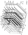
- FIG.1 is an internal perspective view showing an image display apparatus of a first embodiment of the present invention.
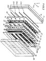
- FIG.2 is an internal perspective view showing an image display apparatus of a second embodiment of the present invention.
- FIG.3(a) is a cross-sectional illustration taken on Y-Z plane in FIG.1.
- FIG.3(b) is a cross-sectional illustration taken on X-Z plane in FIG.1.
- FIG.4 is the cross-sectional illustration taken on X-Z plane in FIG.6.
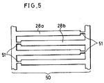
- FIG.5 is a plane view showing a conductive sheet 50 before making a pair of vertical deflection electrodes 28a and 28b.
- FIG.6 is the internal perspective view showing the conventional image display apparatus.
- FIG.1 is an internal perspective view showing an image display apparatus of a first embodiment.
- a back electrode 21, line cathodes 22a, 22b, 22c and 22d, an electron beam extraction electrode 23, a control electrode 24, a first focusing electrode 25, a second focusing electrode 26, a pair of horizontal deflection electrodes 27a and 27b, a pair of vertical deflection electrodes 28a and 28b and a screen 29 are held between a rear plate 31 and a front plate 30 in this order in Z-axis of X-Y-Z coordinates shown in the figure and enclosed by both plates 30 and 31 together with upper and bottom plates (not shown) and side plates (not shown).
- An inside space of the enclosure is evacuated.
- the line cathodes 22a--22d are parallelly disposed to each other in the vertical direction (Y-axis) and fixed by holding means (not shown), and each of the line cathodes 22a--22d is extended in the horizontal direction (X-axis) so that electron-flow of nearly uniform current-density-distribution is produced in the horizontal direction. Although only four pieces of line cathodes 22a--22d are shown in the figure, there are actually many line cathodes (e.g. 24 pieces).
- the line cathodes 22a--22d are made of a tungsten wire and coated with an oxide.
- the back electrode 21 is made of flat plate-shaped conductor and disposed in parallel with the line cathodes 22a--22d.
- the electron beam extraction electrode 23 made of conductive sheet is disposed to oppose against the back electrode 21 across the line cathodes 22a--22d.
- Plural holes 33 are formed in the electron beam extraction electrode 23 and aligned in the horizontal direction at regular intervals to correspond to each line cathode 22a, 22b, 22c or 22d, thereby making matrix arrangement as a whole.
- these holes 33 are circular-shaped in the present embodiment, other shapes of aperture such as ellipse-shaped or rectangular-shaped aperture can be also used.
- the control electrode 24 comprises plural oblong strips 24a, 24b, 24c . . . which are elongated in the vertical (Y-axis) direction and aligned in the horizontal (X-axis) direction at predetermined intervals, thereby forming stripe-shaped configuration on a X-Y plane.
- Plural holes 34 are formed in each of the strips 24a, 24b, 24c . . . at the positions which correspond to the holes 33 of the electron beam extraction electrode 23 in the Z-axis direction, thereby forming the same matrix arrangement on X-Y coordinates as that of the electron beam extraction electrode 23.
- the shape of the holes 34 ellipse or rectangular etc. may be also adopted.
- the first focusing electrode 25 is made of conductive sheet and has plural apertures 35 therein. Each of the apertures 35 is elongated in the horizontal (X-axis) direction to correspond to the line cathodes 22a--22d in the Z-axis direction through the holes 33 and 34.
- the second focusing electrode 26 is also made of conductive sheet and has plural apertures 36 therein. Each of the apertures 36 is elongated in the vertical (Y-axis) direction to correspond to the strips 24a, 24b, 24c . . . in the Z-axis direction.
- the horizontal deflection electrode 27a is made of conductive sheet which is formed into comb-shape comprising comb-teeth parts 37c and a stem part 37a connecting all the comb-teeth parts 37c.
- the horizontal deflection electrode 27b is made of conductive sheet which is formed into comb-shape comprising comb-teeth parts 37d and a stem part 37b connecting all the comb-teeth parts 37d.
- Both horizontal deflection electrodes 27a and 27b are insulatedly disposed to each other on a common X-Y plane in a manner that each of the comb-teeth parts 37c and each of the comb-teeth parts 37d are alternately aligned in parallel with each other (hereinafter is referred as "interdigitated") in the vertical direction. Since potentials applied to both horizontal deflection electrodes 27a and 27b are different from each other, potential difference is given between adjacent two comb-teeth parts 37c and 37d, thereby horizontally deflecting the electron beams 40.
- the vertical deflection electrode 28a is made of conductive sheet which is formed into comb-shape wherein comb-teeth parts 38c and a stem part 38a connecting all the comb-teeth parts 38c are provided.
- the vertical deflection electrode 28b is made of conductive sheet which is formed into comb-shape wherein comb-teeth parts 38d and a stem part 38b connecting all the comb-teeth parts 38d are provided.
- Both vertical deflection electrodes 28a and 28b are insulatedly disposed to each other on a common X-Y plane in a manner that each of the comb-teeth parts 38c and each of the comb-teeth parts 38d are interdigitated with each other in the horizontal direction. Since potentials applied to both vertical deflection electrodes 28a and 28b are different from each other, potential difference is given between adjacent two comb-teeth parts 38c and 38d, thereby vertically deflecting the electron beams 40.
- a fluorescent material layer 39 which emits light by irradiation of the electron beams 40 is coated over an inner surface of the faceplate 30, and thereon a metal-back layer (not shown) is attached, thereby constituting the screen 29.
- Voltage V1 is applied to the back electrode 21 and voltage V2 higher than V1 is applied to the electron beam extraction electrode 23.
- the line cathodes 22a--22d are heated by heater-current in order to easily emit electrons and impressed with voltage V0 (V1 ⁇ V0 ⁇ V2). At that time, electric field on the line cathodes 22a--22d becomes positive to the environment, and thereby the electron beams are emitted and accelerated toward the electron beam extraction electrode 23.
- each of the line cathodes 22a--22d emits the electron beams during a predetermined time period from the upper one (22a) to the bottom one (22d) repeatedly. And thereby, each of the line cathodes 22a--22d forms a sheet-shaped electron beam plane (X-Z plane) having a uniform current-density-distribution in the horizontal direction.
- the above-mentioned sheet-shaped electron beams are divided into plural separate electron beams 40 in the horizontal direction by passing through the holes 33 of the electron beam extraction electrode 23. Thereafter, plural electron beams 40 arrive at the holes 34 of the control electrode 24. Upon this arrival, by setting voltage V3 on the control electrode 24 to have a relation of V3 > V0, the electron beams 40 are allowed to pass through the holes 34, whereas by setting the voltage V3 to be a relation of V3 ⁇ V0, the electron beams 40 lose kinetic energy thereof and cannot pass therethrough. By continuously controlling the voltage V3 in response to video signals, amount of each electron beam 40 which passes through the holes 34 is controlled.
- the electron beams 40 After passing through the control electrode 24, the electron beams 40 arrive at the first focusing electrode 25. At that time, the electron beams 40 are focused in the direction of Y-axis by electrostatic-lens-effect presented by the apertures 35. Next, the electron beams 40 arrive at the second focusing electrode 26 and are accelerated toward the direction of Z-axis by potential applied to the second focusing electrode 26. Further, the electron beams 40 are shaped by passing through the second focusing electrode 26. After that, the electron beams 40 arrive at the horizontal deflection electrodes 27a and 27b and are focused in the direction of X-axis by electrostatic-lens-effect of the horizontal deflection electrodes 27a and 27b.
- the electron beams 40 are electrostatically deflected in the direction of X-axis in response to the potential difference.
- the electron beams 40 arrive at the vertical deflection electrodes 28a and 28b and are focused in the direction of Y-axis by electrostatic-lens-effect of the vertical deflection electrodes 28a and 28b.
- potential difference deflection voltage
- the electron beams 40 are electrostatically deflected in the direction of Y-axis in response to the potential difference.
- the electron beams 40 are accelerated to have high energy by high voltage (e.g. 10kV) applied to the metal-back layer of the screen 29. These electron beams 40 having high energy collide with the metal-back layer, thereby emitting light from the fluorescent material layer 39.
- high voltage e.g. 10kV
- the screen 29 are horizontally and vertically divided into the matrix arrangement of plural sectional screen 41.
- Each of the sectional screens 41 is scanned by deflecting one electron beam which is separated from other electron beams. Thereby, the whole image is displayed on the screen 29.
- R, G and B video signals corresponding to respective picture elements are continuously controlled by the voltage applied to the control electrode 24, and thereby television image is reproduced.
- FIG.2 is an internal perspective view showing the image display apparatus of a second embodiment.
- first focusing electrode 25 and the second focusing electrode 26 rectangular holes 45 and 46 are formed into matrix arrangements, respectively. Positions of the holes 45 and 46 in a X-Y plane correspond to the holes 33 of the electron beam extraction electrode 23 and the holes 34 of the control electrode 24.
- the hole 45 is elongated in the horizontal (X-axis) direction and the hole 46 is elongated in the vertical (Y-axis) direction.
- Electrostatic-lens-effects on respective center positions of the holes 45 and 46 are substantially equal to those of the apertures 35 and 36 in FIG.1, respectively.
- every parts which constitute the image display apparatus are thin plate-shaped or sheet-shaped. Depth (in Z-axis) of the image display apparatus is thereby shortened as a whole, and a flat screen is offered.
- FIG.3(a) is a cross-sectional illustration taken on a plane Y-Z in FIG.1
- FIG.3(b) is a cross-sectional illustration taken on a plane X-Z in FIG.1.
- Corresponding parts to FIG.1 are shown by the same numerals and marks, and the description thereon made in FIG.1 similarly applies.
- Thermions having initial velocity responding to heat energies thereof are nondirectionally emitted from around the line cathode 22a. Therefore, there exist not only a flow of electron beam 40a but also another flow of electron beam 40b. That is, some thermions emitted from the line cathode 22a obliquely enters the hole 33 of the electron beam extraction electrode 23 as shown by the electron beam 40b.
- the voltage V2 of the electron beam extraction electrode 23 the voltage V3 of the control electrode 24 and the voltage V4 of the first focusing electrode 25 are set to be nearly equal to each other and the voltage V5 of the second focusing electrode 26 is set to be considerably higher than the voltages V2, V3 and V4, electric-field-gap is formed in the aperture 35 (FIG.1) of the first focusing electrode 25.
- the aperture 35 is narrow and long in the direction of X-axis, electrostatic-focusing-effect is effective only in the direction of Y-axis and electric field is little changed in the direction of X-axis.
- the electron beams 40a and 40b are accelerated toward the direction of Z-axis by the voltage of the second focusing electrode 26 without focusing, thereby desirably fixing electron flow.
- the horizontal deflection electrodes 27a and 27b provide electrostatic-focusing-effect only in the direction of X-axis by setting the voltage V6 of the horizontal deflection electrodes 27a and 27b to be lower than the voltage V5, thereby obtaining a beam spot of horizontally (i.e. on X-Z plane) minimum diameter d on the screen 29. A desirable small beam spot is thus realized.
- FIG.4 is a cross-sectional illustration taken on an X-Z plane of the conventional image display apparatus shown in FIG.6.
- a cross-sectional illustration taken on a Y-Z plane is similar to FIG.3(a).
- an electrostatic lens is formed in the hole 13 of the focusing electrode 5 on the X-Z plane owing to the fact that apertures of the first focusing electrode 5 are circular holes 13, oblique electron beam 40b is focused before fixing of travelling direction toward the direction of Z-axis. Consequently, position of a focus 41a of the electron beam 40a is away from that of a focus 41b of the electron beam 40b on the screen 9. Thereby, a diameter D of beam spot on the horizontal (X-Z) plane is enlarged, and quality of image is deteriorated.
- the vertical deflection electrodes 28a and 28b in the present invention are disposed in the final step to pass the electron beam.
- the vertical deflection electrode 6 is disposed before the horizontal deflection electrode 7 as shown in FIG.4
- vertical focusing of the electron beams becomes dull because the subsequent horizontal deflection electrode 7 undesirably has a slight influence on the electron beams in the vertical direction, thereby resulting in decline of sensitivity of deflection. It is possible to decrease such an influence by limiting deflection angle.
- the above-mentioned disposition of the present invention is advantageous to precisely deflect the electron beam in the vertical direction, and thereby excellent sensitivity of deflection is obtained.
- control electrode 24 comprising plural conductive sheets.
- the control electrode 24 is made of one sheet wherein plural strips and crosspieces connecting the strips are provided by etching.
- respective electrodes 23--28a, 28b are fixedly laminated with insulation spacers put therebetween.
- the crosspieces are removed by irradiating laser beam, thereby making a stripe-shaped control electrode 24.
- respective electrodes are precisely worked and assembled with low manufacturing cost.
- FIG.5 is a plane view showing a conductive sheet 50 before making a pair of vertical deflection electrodes 28a and 28b.
- a piece of conductive sheet 50 is formed by etching pattern into the configuration shown in the figure, wherein the vertical deflection electrode 28a and the vertical deflection electrode 28b are connected with each other via thin crosspieces 51.
- respective electrodes 23--28a, 28b (FIG.1) are laminated and fixed.
- the crosspieces 51 are removed by irradiating laser beam, thereby making a pair of comb-shaped vertical deflection electrodes 28a and 28b which are isolated from each other.
Landscapes
- Cathode-Ray Tubes And Fluorescent Screens For Display (AREA)
Claims (6)
- Eine Bildanzeigevorrichtung, die aufweist:
eine Vielzahl von Linienkathoden (22a-22d), die parallel miteinander verlaufen, um Elektronen auszusenden;
eine Elektronenstrahlextraktionselektrode (23) zum Extrahieren bzw. Ausziehen von Elektronenstrahlen aus den Linienkathoden;
eine Steuerelektrode (24) zum wahlweisen Steuern der Durchtrittsmenge von Elektronenstrahlen, die durch die Elektronenstrahlextraktionselektrode hindurchgetreten sind;
eine Fokussierelektrodeneinrichtung (25,26) zum elektrostatischen Fokussiereen von Elektronenstrahlen, die durch die Steuerelektrode hindurchgetreten sind;
eine Ablenkelektrodeneinrichtung (27a,27b,28a,28b) zum Ablenken von Elektronenstrahlen, die durch die Fokussierelektrodeneinrichtung (25,26) hindurchgelangt sind, wobei die Ablenkelektrodeneinrichtung eine Horizontalablenkelektrode (27a,27b) zum elektrostatischen Ablenken von Elektronenstrahlen in einer verlängerten Richtung der Linienkathoden aufweist; und
eine Vertikalablenkelektrode (28a,28b) zum elektrostatischen Ablenken von Elektronenstrahlen in einer zu der verlängerten Richtung der Linienkathoden senkrechten Richtung; und
eine Anzeigeeinrichtung (29) zum Aussenden von Licht durch Empfangen von Elektronenstrahlen, die durch die Vertikalablenkelektrode hindurchgelangt sind;
wobei die oben genannten Komponenten in dieser Reihenfolge angeordnet sind,
dadurch gekennzeichnet, daß in der Ablenkelektrodeneinrichtung (27a,27b,28a,28b)
die Horizontalablenkelektrode (27a,27b) angeordnet ist, um Elektronenstrahlen abzulenken, die durch die Fokussierelektrodeneinrichtung (25,26) gelangt sind, und
die Vertikalablenkelektrode (28a,28b) angeordnet ist, um Elektronenstrahlen abzulenken, die durch die Horizontalablenkelektrode (27a,27b) gelangt sind. - Eine Bildanzeigevorrichtung nach Anspruch 1, dadurch gekennzeichnet, daß die Fokussierelektrodeneinrichtung eine leitfähige Platte oder Scheibe aufweist, wobei eine Vielzahl von länglichen Öffnungen (35,45), die sich in einer verlängerten Richtung der Linienkathoden erstrecken, ausgebildet ist.
- Eine Bildanzeigevorrichtung nach Anspruch 2, dadurch gekennzeichnet, daß
die Fokussierelektrodeneinrichtung eine erste Fokussierelektrode (25) aufweist, die aus der leitenden Scheibe gebildet ist, in der die Vielzahl von Öffnungen (35,45) ausgebildet ist,
wobei die Öffnungen (35,45) längliche Öffnungen (35,45) sind, die sich in einer verlängerten Richtung der Linienkathoden (22a-22d) erstrecken, und
daß die Fokussierelektrodeneinrichtung eine zweite Fokussierelektrode (26) zum elektrostatischen Fokussieren von Elektronenstrahlen, die durch die erste Fokussierelektrode gelangt sind, in der verlängerten Richtung der Linienkathoden (22a-22d) aufweist. - Eine Bildanzeigevorrichtung nach Anspruch 3, dadurch gekennzeichnet, daß die zweite Fokussierelektrode (26) aus einer leitenden Scheibe oder Platte hergestellt ist, wobei eine Vielzahl von länglichen Öffnungen (36,46) sich in einer zu der verlängerten Richtung der Linienkathoden senkrechten Richtung erstreckt.
- Eine Bildanzeigevorrichtung nach einem der Ansprüche 1 bis 4, dadurch gekennzeichnet, daß die Horizontalablenkelektrode ein Paar von kammförmigen leitenden Scheiben (27a,27b) oder Platten aufweist, die in einer vertikalen Richtung auf der gleichen Ebene miteinander isoliert kammartig verschachtelt sind.
- Eine Bildanzeigevorrichtung nach einem der Ansprüche 1 bis 5, dadurch gekennzeichnet, daß die Vertikalablenkelektrode ein Paar von kammförmigen leitenden Scheiben (28a,28b) aufweist, die miteinander in einer Horizontalrichtung auf der gleichen Ebene isoliert kammartig verschachtelt sind.
Applications Claiming Priority (4)
| Application Number | Priority Date | Filing Date | Title |
|---|---|---|---|
| JP62288762A JPH01130453A (ja) | 1987-11-16 | 1987-11-16 | 画像表示装置 |
| JP288762/87 | 1987-11-16 | ||
| JP184962/88 | 1988-07-25 | ||
| JP63184962A JPH0233839A (ja) | 1988-07-25 | 1988-07-25 | 画像表示装置 |
Publications (3)
| Publication Number | Publication Date |
|---|---|
| EP0316871A2 EP0316871A2 (de) | 1989-05-24 |
| EP0316871A3 EP0316871A3 (en) | 1990-01-10 |
| EP0316871B1 true EP0316871B1 (de) | 1994-11-30 |
Family
ID=26502816
Family Applications (1)
| Application Number | Title | Priority Date | Filing Date |
|---|---|---|---|
| EP88119027A Expired - Lifetime EP0316871B1 (de) | 1987-11-16 | 1988-11-15 | Bildwiedergabevorrichtung |
Country Status (3)
| Country | Link |
|---|---|
| US (1) | US4955681A (de) |
| EP (1) | EP0316871B1 (de) |
| DE (1) | DE3852276T2 (de) |
Families Citing this family (28)
| Publication number | Priority date | Publication date | Assignee | Title |
|---|---|---|---|---|
| JPH02306527A (ja) * | 1989-05-19 | 1990-12-19 | Matsushita Electric Ind Co Ltd | 平板型画像表示装置 |
| US5160871A (en) * | 1989-06-19 | 1992-11-03 | Matsushita Electric Industrial Co., Ltd. | Flat configuration image display apparatus and manufacturing method thereof |
| US5189335A (en) * | 1989-10-20 | 1993-02-23 | Matsushita Electric Industrial Co., Ltd. | Method of controlling electron beams in an image display apparatus |
| CN1026943C (zh) * | 1990-03-06 | 1994-12-07 | 杭州大学 | 平板彩色显示器 |
| JP2590618B2 (ja) * | 1990-05-31 | 1997-03-12 | 松下電器産業株式会社 | 画像表示装置 |
| JPH04169047A (ja) * | 1990-11-01 | 1992-06-17 | Matsushita Electric Ind Co Ltd | 表示装置 |
| US5859508A (en) * | 1991-02-25 | 1999-01-12 | Pixtech, Inc. | Electronic fluorescent display system with simplified multiple electrode structure and its processing |
| WO1994011896A1 (fr) * | 1992-11-06 | 1994-05-26 | Mitsubishi Denki Kabushiki Kaisha | Affichage d'images |
| JPH0745218A (ja) * | 1993-05-26 | 1995-02-14 | Matsushita Electric Ind Co Ltd | 平面型画像表示装置 |
| US5446337A (en) * | 1993-07-28 | 1995-08-29 | Matsushita Electric Industrial Co., Ltd. | Image display apparatus and method of making the same |
| JP3119052B2 (ja) * | 1993-09-30 | 2000-12-18 | 松下電器産業株式会社 | 平板状画像表示装置 |
| JP3189531B2 (ja) * | 1993-10-01 | 2001-07-16 | 松下電器産業株式会社 | 平板電極ユニットおよびその製造方法 |
| GB2285168B (en) * | 1993-12-22 | 1997-07-16 | Marconi Gec Ltd | Electron field emission devices |
| GB2304984B (en) * | 1995-08-25 | 1999-08-25 | Ibm | Electron source |
| GB2304981A (en) * | 1995-08-25 | 1997-03-26 | Ibm | Electron source eg for a display |
| JP2001523375A (ja) | 1995-10-26 | 2001-11-20 | ピックステック インコーポレイテッド | 冷陰極電界放出極フラットスクリーンディスプレイ |
| US6208072B1 (en) | 1997-08-28 | 2001-03-27 | Matsushita Electronics Corporation | Image display apparatus with focusing and deflecting electrodes |
| JP3457162B2 (ja) | 1997-09-19 | 2003-10-14 | 松下電器産業株式会社 | 画像表示装置 |
| US6630782B1 (en) * | 1997-12-01 | 2003-10-07 | Matsushita Electric Industrial Co., Ltd. | Image display apparatus having electrodes comprised of a frame and wires |
| US6236381B1 (en) * | 1997-12-01 | 2001-05-22 | Matsushita Electronics Corporation | Image display apparatus |
| US6441543B1 (en) * | 1998-01-30 | 2002-08-27 | Si Diamond Technology, Inc. | Flat CRT display that includes a focus electrode as well as multiple anode and deflector electrodes |
| US6509687B1 (en) * | 1999-11-30 | 2003-01-21 | International Business Machines Corporation | Metal/dielectric laminate with electrodes and process thereof |
| KR100453294B1 (ko) * | 2002-03-12 | 2004-10-15 | 엘지.필립스디스플레이(주) | 평판형 디스플레이 장치의 수평 편향 전극 구조 |
| JP5243793B2 (ja) * | 2004-07-05 | 2013-07-24 | シーイービーティー・カンパニー・リミティッド | マルチマイクロコラムにおける電子ビームの制御方法及びこの方法を利用したマルチマイクロコラム |
| KR100926748B1 (ko) * | 2004-08-11 | 2009-11-16 | 전자빔기술센터 주식회사 | 멀티 에스에프이디 |
| US20080012461A1 (en) * | 2004-11-09 | 2008-01-17 | Nano-Proprietary, Inc. | Carbon nanotube cold cathode |
| US20100024353A1 (en) * | 2008-07-29 | 2010-02-04 | Green Horizon Manufacturing Llc | Method for deploying prefabricated structures arranged in a complementary layout |
| CN114068267B (zh) * | 2020-08-04 | 2023-03-28 | 清华大学 | 偏转电极组件、x射线源和x射线成像系统 |
Family Cites Families (5)
| Publication number | Priority date | Publication date | Assignee | Title |
|---|---|---|---|---|
| JPS5853462B2 (ja) * | 1976-09-20 | 1983-11-29 | 松下電器産業株式会社 | 画像表示装置 |
| US4227117A (en) * | 1978-04-28 | 1980-10-07 | Matsuhita Electric Industrial Co., Ltd. | Picture display device |
| JPS5772234A (en) * | 1980-10-20 | 1982-05-06 | Matsushita Electric Ind Co Ltd | Production of electrode structure |
| KR850000970B1 (ko) * | 1981-02-10 | 1985-07-02 | 야마시다 도시히꼬 | 화상표시 장치 |
| KR850000958B1 (ko) * | 1981-02-10 | 1985-06-29 | 야마시다 도시히꼬 | 화상표시장치 |
-
1988
- 1988-11-15 EP EP88119027A patent/EP0316871B1/de not_active Expired - Lifetime
- 1988-11-15 DE DE3852276T patent/DE3852276T2/de not_active Expired - Fee Related
- 1988-11-16 US US07/271,821 patent/US4955681A/en not_active Expired - Lifetime
Also Published As
| Publication number | Publication date |
|---|---|
| US4955681A (en) | 1990-09-11 |
| EP0316871A2 (de) | 1989-05-24 |
| EP0316871A3 (en) | 1990-01-10 |
| DE3852276D1 (de) | 1995-01-12 |
| DE3852276T2 (de) | 1996-01-04 |
Similar Documents
| Publication | Publication Date | Title |
|---|---|---|
| US4955681A (en) | Image display apparatus having sheet like vertical and horizontal deflection electrodes | |
| EP0079108B1 (de) | Bildröhre | |
| EP0982756A1 (de) | Flache Anzeigetafel mit Mikro-Elektronenlinsenstruktur | |
| EP0434054B1 (de) | Flache Bildanzeigevorrichtung | |
| US20040227452A1 (en) | Field emission display having grid plate | |
| JP2982222B2 (ja) | 平面型表示装置 | |
| JP2754546B2 (ja) | 画像表示装置 | |
| EP0631296B1 (de) | Apparat für Flachbildwiedergabe | |
| JPH0233839A (ja) | 画像表示装置 | |
| EP0143669B1 (de) | Bildwiedergabevorrichtung | |
| JP3189513B2 (ja) | 画像表示装置の製造方法 | |
| JP2830190B2 (ja) | 画像表示装置 | |
| JP2890572B2 (ja) | 平面型表示装置 | |
| JP2549108B2 (ja) | 受像管装置 | |
| JP3082290B2 (ja) | 平面型表示装置 | |
| JP3158868B2 (ja) | 画像表示装置 | |
| KR940009191B1 (ko) | 평면형 냉음극선관 | |
| JP2890571B2 (ja) | 平面型表示装置 | |
| JPH01130453A (ja) | 画像表示装置 | |
| JPS59146142A (ja) | 平板型画像表示装置 | |
| JPH06139925A (ja) | 画像表示装置の製造方法 | |
| JPH05182584A (ja) | 画像表示装置の製造方法 | |
| JPH07335151A (ja) | 平板型画像表示装置 | |
| JPH07176279A (ja) | 平板型画像表示装置 | |
| JPH05182585A (ja) | 画像表示装置の製造方法 |
Legal Events
| Date | Code | Title | Description |
|---|---|---|---|
| PUAI | Public reference made under article 153(3) epc to a published international application that has entered the european phase |
Free format text: ORIGINAL CODE: 0009012 |
|
| 17P | Request for examination filed |
Effective date: 19881115 |
|
| AK | Designated contracting states |
Kind code of ref document: A2 Designated state(s): DE FR GB |
|
| PUAL | Search report despatched |
Free format text: ORIGINAL CODE: 0009013 |
|
| AK | Designated contracting states |
Kind code of ref document: A3 Designated state(s): DE FR GB |
|
| 17Q | First examination report despatched |
Effective date: 19920323 |
|
| GRAA | (expected) grant |
Free format text: ORIGINAL CODE: 0009210 |
|
| AK | Designated contracting states |
Kind code of ref document: B1 Designated state(s): DE FR GB |
|
| REF | Corresponds to: |
Ref document number: 3852276 Country of ref document: DE Date of ref document: 19950112 |
|
| ET | Fr: translation filed | ||
| PLBE | No opposition filed within time limit |
Free format text: ORIGINAL CODE: 0009261 |
|
| STAA | Information on the status of an ep patent application or granted ep patent |
Free format text: STATUS: NO OPPOSITION FILED WITHIN TIME LIMIT |
|
| PGFP | Annual fee paid to national office [announced via postgrant information from national office to epo] |
Ref country code: GB Payment date: 19951106 Year of fee payment: 8 |
|
| PGFP | Annual fee paid to national office [announced via postgrant information from national office to epo] |
Ref country code: FR Payment date: 19951109 Year of fee payment: 8 |
|
| PGFP | Annual fee paid to national office [announced via postgrant information from national office to epo] |
Ref country code: DE Payment date: 19951113 Year of fee payment: 8 |
|
| 26N | No opposition filed | ||
| PG25 | Lapsed in a contracting state [announced via postgrant information from national office to epo] |
Ref country code: GB Effective date: 19961115 |
|
| GBPC | Gb: european patent ceased through non-payment of renewal fee |
Effective date: 19961115 |
|
| PG25 | Lapsed in a contracting state [announced via postgrant information from national office to epo] |
Ref country code: FR Effective date: 19970731 |
|
| PG25 | Lapsed in a contracting state [announced via postgrant information from national office to epo] |
Ref country code: DE Effective date: 19970801 |
|
| REG | Reference to a national code |
Ref country code: FR Ref legal event code: ST |