EP0317464B1 - Dispositif intermédiaire enfichable et support de carte de circuit imprimé - Google Patents
Dispositif intermédiaire enfichable et support de carte de circuit imprimé Download PDFInfo
- Publication number
- EP0317464B1 EP0317464B1 EP88480024A EP88480024A EP0317464B1 EP 0317464 B1 EP0317464 B1 EP 0317464B1 EP 88480024 A EP88480024 A EP 88480024A EP 88480024 A EP88480024 A EP 88480024A EP 0317464 B1 EP0317464 B1 EP 0317464B1
- Authority
- EP
- European Patent Office
- Prior art keywords
- enclosure
- circuit card
- connector
- interposer assembly
- housing
- Prior art date
- Legal status (The legal status is an assumption and is not a legal conclusion. Google has not performed a legal analysis and makes no representation as to the accuracy of the status listed.)
- Expired
Links
Images



Classifications
-
- H—ELECTRICITY
- H05—ELECTRIC TECHNIQUES NOT OTHERWISE PROVIDED FOR
- H05K—PRINTED CIRCUITS; CASINGS OR CONSTRUCTIONAL DETAILS OF ELECTRIC APPARATUS; MANUFACTURE OF ASSEMBLAGES OF ELECTRICAL COMPONENTS
- H05K9/00—Screening of apparatus or components against electric or magnetic fields
- H05K9/0062—Structures of standardised dimensions, e.g. 19" rack, chassis for servers or telecommunications
-
- H—ELECTRICITY
- H05—ELECTRIC TECHNIQUES NOT OTHERWISE PROVIDED FOR
- H05K—PRINTED CIRCUITS; CASINGS OR CONSTRUCTIONAL DETAILS OF ELECTRIC APPARATUS; MANUFACTURE OF ASSEMBLAGES OF ELECTRICAL COMPONENTS
- H05K7/00—Constructional details common to different types of electric apparatus
- H05K7/14—Mounting supporting structure in casing or on frame or rack
- H05K7/1461—Slidable card holders; Card stiffeners; Control or display means therefor
-
- Y—GENERAL TAGGING OF NEW TECHNOLOGICAL DEVELOPMENTS; GENERAL TAGGING OF CROSS-SECTIONAL TECHNOLOGIES SPANNING OVER SEVERAL SECTIONS OF THE IPC; TECHNICAL SUBJECTS COVERED BY FORMER USPC CROSS-REFERENCE ART COLLECTIONS [XRACs] AND DIGESTS
- Y10—TECHNICAL SUBJECTS COVERED BY FORMER USPC
- Y10S—TECHNICAL SUBJECTS COVERED BY FORMER USPC CROSS-REFERENCE ART COLLECTIONS [XRACs] AND DIGESTS
- Y10S174/00—Electricity: conductors and insulators
- Y10S174/34—PCB in box or housing
Definitions
- This invention relates generally to a shielded, plugable, mounting enclosure for printed circuit cards such as used in a computer.
- Improvements in semiconductor technology have contributed to a manyfold increase in the number of electronic devices used in everyday life.
- the reduced size and cost of transistors and integrated circuits have made many electronic devices virtual necessities to every day life.
- the expansion of electronic devices has occurred in the work place as well as the home, bringing people with virtually no electronic experience or skills into contact as purchasers and users.
- DE-A-3 604 860 describes an arrangement for electromagnetically shielding a plurality of pluggable electric elements, each of which comprises a grounding spring for engaging the inner surface of the invention.
- EP-A-188 968 describes a write/read device comprising several pluggable electronic memory modules comprising a locking mechanism.
- the principle object of the invention is to provide a shielded interposer assembly as defined in claim 1.
- This invention provides a package for large and small printed circuit cards, easily handled and plugged by the unskilled user, which provides a very high degree of electromagnetic shielding and can serve as an interposer to accommodate the connection of cables as well.
- the package includes a book-like housing, which can totally enclose and shield a circuit card, adapted to be plugged into a host assembly such as a computer backplane.
- the housing is easily adapted to polarization to prevent individual housings from being plugged into inappropriate slots in the backplane.
- the housing may include camming handles which serve to force the housing into the receiving socket, hold the housing in place after plugging, and serve to cam the housing out of the socket when the housing is to be removed.
- the housing includes a socket adapted for the connection of additional card enclosures or cables.
- the housing has accommodation for the flow of cooling air over the enclosed circuit card to prevent overheating.
- Fig. 1 is a partial isometric view of a portion of an assembly showing a plugable printed circuit card enclosure according to the invention.
- Fig. 1a is a partial front view of the right rear corner of the system backplane showing the arrangement of the connector and grounding springs.
- Fig. 1b is a sectional view of a grounding spring shown in Fig. 1a taken along the line 1b-1b.
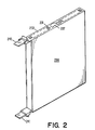
- Fig. 2 is an isometric view of a plugable printed circuit card enclosure according to the invention.
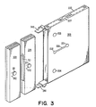
- Fig. 3 is an isometric view of a plugable printed circuit card enclosure according to the invention wherein multiple cards may be serially plugged into the enclosure.
- Fig. 4 is an isometric view of a plugable printed circuit card enclosure according to the invention wherein multiple cards may be adjacently plugged into the enclosure.
- Fig. 5 is an isometric view of a plugable printed circuit card enclosure according to the invention wherein multiple cards may be plugged into the enclosure and held in position with a lever type latch which assists in the plugging and unplugging operation.
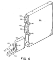
- Fig. 6 is an isometric view of a plugable printed circuit card enclosure according to the invention wherein multiple cards may be plugged into the enclosure for the accommodation of plugable printed circuit card enclosures shown in Fig. 5.
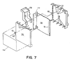
- Fig. 7 is an exploded view of a smaller pluggable printed circuit card enclosure showing the arrangement of the printed circuit card and identifying label.
- a computer backplane assembly comprises an enclosure 1 having a plurality of positions for card enclosures separated by guide rails 2. Cooling air holes 3 are located on the top surface 5 and the bottom surface 6. The rear of the enclosure 1 includes a plurality of connectors and grounding springs as shown in Fig. 1a.
- a connector is positioned to accept a complementary connector 21 on a plugable card assembly 20.
- a plurality of grounding springs 12 are positioned around the connector to provide shielding.
- the shape of grounding springs 12 is shown in Fig. 1b, which is a partial sectional view taken along the line 1b-1b of Fig. 1a.
- Each of the grounding springs 12 has a curved portion 13 which is deflected backwardly toward rear wall 14 by the rear surface of the plugable enclosure.
- the grounding springs 12 are fastened to the rear wall 14 by appropriate fasteners such as screws 15 which pass through the flat portion 16.
- Plugable card assembly 20 is adapted to fit between the guide rails 2. If it is desired to restrict the plugable card assembly 20 to a single plug position, suitable keys can be provided on the enclosure 1 to prevent misplugging. For example, an enlarged corner key 25, which is adapted to fit a plugable card assembly having the upper left corner recessed to fit the corner key 25, can be provided to prevent plugging of assemblies which lack the correct key.
- the plugable card assembly 20 includes a back, or first end, 30 on which the complementary connector 21 is mounted.
- the back end 30 is essentially flat to provide a good grounding surface for grounding springs 12.
- the top 31 of the enclosure contains a plurality of openings 32 having a maximum dimension of 2,54 cm (one inch) to accommodate the flow of cooling air.
- the bottom 35 contains a plurality of openings 36 to accommodate the flow of cooling air. Suitable means, such as a fan, may be used to force cooling air through the cooling air holes 3, the plugable card assembly 20 and out the openings 36.
- a grounding spring 37 is positioned on the top of plugable card assembly 20 for engaging the inner surface of the enclosure 1, and providing an improved connection to ground for shielding purposes.
- a printed circuit card 84 having connections to complementary connector 21, is mounted within plugable card assembly 20.
- the embodiment shown in Fig. 1 is illustrative of an embodiment in which the circuit card occupies only a portion of the plugable card assembly 20. Alternatively, the circuit card can occupy the entire enclosure, in which case the open front portion 38 would be replaced with a solid face as will be later described.
- a pair of handles 40 and 41 are pivotally mounted on bosses supported by projections 43 extending from the sides of plugable card assembly 20. These handles may be used to disengage the enclosure from the backplane by forcing handle 40 upwardly and handle 41 downwardly. The shorter portions 45 and 46 are thus brought to bear against the abutting front surface of the enclosure 1 and serve to cam the enclosure for disengagement with the enclosure 1.
- a smaller, plugable "daughter" printed circuit card enclosure 60 is adapted to fit with the plugable card assembly 20 and make contact with the connector 61, mounted on partition 64 by means of a complementary connector, not shown, on the rear of the assembly.
- Enclosure 60 has holes 63 in the top surface 62, which coact with the openings 32 to provide a flow of cooling air over the electronic circuitry within the enclosure.
- the bottom surface of enclosure 60 also contains holes, not shown, for the passage of cooling air.
- a handle 65 pivoted at points 66 and 67, has a pair of ears 70 and 71 which coact with the slots 72 and 73 in the sides of plugable card assembly 20.
- the enclosure 60 is pushed inwardly until the ends of ears 70 and 71 come to bear against the back edge of slots 72 and 73. At this point the finger tab 74 is moved upwardly, causing the ears 70 and 71 to bear against the inner edges 80 and 81 of slots 72 and 73. Continued movement of finger tab 74 in the clockwise direction causes the pivot points 66 and 67 to cam against the inner edges 80 and 81 and force the connector of enclosure 60 into engagement with connector 61.
- Fig. 2 shows an alternative form of enclosure for plugging into the enclosure 1.
- the printed circuit card enclosure 200 is proportioned to accommodate a larger card than the enclosure 60 previously described. Typical of such a larger card would be the card containing the processor circuitry or basis increment of memory for a small computer.
- the enclosure 200 contains no accommodation for the plugging of additional enclosures and therefore has a solid cover throughout.
- the enclosure 200 would be plugged into a slot similar to the slot which receives the plugable card assembly 20.
- the enclosure 200 has a grounding spring 237 on the top for coaction with the inner portion of the top of backplane assembly 1.
- Enclosure 200 also has handles 240 and 241 which serve the same purpose as the comparable elements of plugable card assembly 20.
- the shape of the holes 231 in the top 232 of enclosure 200 is somewhat different than the shape of the openings 32 in the plugable card assembly 20.
- the smaller, thinner holes may be desired when the circuitry contained within the enclosure is more sensitive to interference or has a greater tendency to emit radiation in an undesired spectrum.
- Fig. 3 is illustrative of another embodiment of the plugable enclosure. It is desirable in some circumstances to provide a "piggyback" arrangement for optional printed circuit cards when those added later must rely on certain circuit features in earlier added cards, or where a plurality of cards share a common bus, such as memory cards.
- the basic enclosure 300 occupies the full depth of the enclosure 1. It has the same type of holes 332 in the top for air flow and the same type of handles 340 and 341 for extraction of the enclosure from the backplane.
- the front of the enclosure 300 has an opening of sufficient width to accommodate the insertion of the smaller plugable assemblies 320 and 330, each of which may have a suitable connector 321 and a connector on the back of enclosure 320 which is not shown.
- a slot 350 in the side of enclosure 300 has a pair of holes 351 and 352 at the extremities.
- the holes are slightly larger than the corresponding buttons 371 and 381 on enclosures 320 and 330, respectively.
- Each of the buttons is mounted on a flexible tab portion of the side of the smaller enclosure.
- Tab portion 372 of enclosure 320 allows the button 371, and its counterpart on the opposite side of enclosure 320, to be deflected inwardly to allow the enclosure 320 to be inserted into the open end of the enclosure 300.
- the smaller enclosure is pushed into the larger until the connector, not shown, mates with the connector, not shown, on the inside of enclosure 300.
- button 371 lines up with slot 351 and pops out into slot 351 to retain the enclosure 320 in place. It will be appreciated that the button 371 will first pop out into the hole 352 and must be again deflected inwardly to allow completion of the insertion process.
- the enclosure 330 may then be inserted into enclosure 300 in like fashion, locking into place when the button 381, on tab 382, pops out into hole 352.
- Removal of the piggyback enclosures is accomplished by depressing the buttons, inwardly to disengage them from the holes and urging the enclosure outwardly.
- the additional holes 353 and 354 are positioned to accommodate three piggyback enclosures having one third the length of those shown. Each one of the enclosures would then latch into one of the holes 352, 353, and 354.
- FIG. 4 A further alternative embodiment of plugable enclosure is shown in Fig. 4.
- the top 431 of enclosure 400 has a plurality of air holes 432.
- Latches 440 and 441 provide the same function as previously described.
- a grounding spring 437 functions in the same manner as that for the earlier described embodiments.
- the enclosure 400 is designed to accommodate the plugging of three smaller enclosures 470, 480 and 490.
- Each of these smaller enclosures has the same sort of locking buttons 471, 481 and 491 as that described with reference to the embodiment of Fig. 3.
- the locking buttons are mounted on flexible tongues 472, 482 and 492, respectively, to allow them to be deflected inwardly during the process of insertion into enclosure 400.
- the front of enclosure 400 has three cut-out portions 401, 402 and 403 to provide an area where the fingers can easily grasp the enclosure 470, 480 and 490 during the insertion and removal process.
- the holes 453, 452 and 454 coact with the buttons 471, 481 and 491 to lock the smaller enclosures in place.
- one of the enclosures may have a socket 460 for the connection of a cable leading to a printer or other peripheral device.
- guide rails 410 and 411 are located with the enclosure 400 to accurately position the individual smaller enclosures as they slid into place.
- Fig. 5 shows a larger plugable enclosure 500 with one smaller enclosure 520 in position for insertion and one smaller enclosure 530 in the plugged position, illustrating the manner in which the handle 565 locks the enclosure in the plugged position.
- the embodiment of Fig. 6 is similar to that of Figs. 4 and 5.
- the larger plugable enclosure 600 includes a provision for insertion of a variety of smaller plugable enclosures 620, 630, and 640, each of which has a corresponding slot 621, 631, and 641 in the side walls of enclosure 600 for the locking handles 623, 633 and 643, respectively.
- the connector 626 is plugged into socket 627 after insertion of the enclosure 620 into enclosure 600 and after handle 623 is locked in place as described with reference to Fig. 1. This locks enclosure 620 in place and it cannot be removed without first removing connector 626 from socket 627. This is desirable because of the adverse effect on system operation caused by the inadvertent disconnection of an I/O module such as contained in enclosure 620 during operation of a system.
- the error condition caused by such disconnection is one from which a typical computer system has a difficult time recovering, and it is therefore desirable to avoid.
- Fig. 7 is an exploded view of a smaller plugable enclosure such as enclosure 520 shown in Fig. 5.
- This enclosure is suitable for holding a printed circuit card for the implantation of a feature which may be optional. That is, a standard minimum computer configuration might not require inclusion of the feature contained in this enclosure.
- the enclosure includes a left side 710, a right side 720, and a printed circuit card 730 mounted in the front 740.
- the circuit card 730 is spaced from side 710 by molding projections 711 and 712.
- a plurality of holes 731 connected to handles, not shown, on the circuit board 730 accommodate the lead wires to a connector mounted on the back of the enclosure.
- the handle 750 is pivotally mounted on bosses 751 extending from the ears 752. Holes for cooling air are provided by the opposing interlocking fingers 723 and 713 on sides 720 and 710, respectively.
- a label 760 may be affixed to the side 720 for identification purposes.
Landscapes
- Engineering & Computer Science (AREA)
- Microelectronics & Electronic Packaging (AREA)
- Mounting Of Printed Circuit Boards And The Like (AREA)
- Cooling Or The Like Of Electrical Apparatus (AREA)
- Shielding Devices Or Components To Electric Or Magnetic Fields (AREA)
- Details Of Connecting Devices For Male And Female Coupling (AREA)
- Coupling Device And Connection With Printed Circuit (AREA)
Claims (8)
- Dispositif interposeur (20), contenant une carte de circuit, pour connexion d'une carte de circuit supplémentaire ou d'un câble à un plan de fond de système, caractérisé en ce qu'il comprend :(a) un boîtier métallique d'interposition, comportant une paroi supérieure (31), une paroi inférieure (35), des parois latérales, une paroi arrière (30) et un premier connecteur (21) placé sur sa dite paroi arrière pour accouplement et connexion avec le plan de fond du système ;(b) un deuxième connecteur (61) fixé à une cloison (64), positionné à l'intérieur dudit boîtier et connecté à ladite carte de circuit (84) qui y est contenue, ladite cloison étant un élément métallique solide qui coopère avec lesdites parois latérales et ladite paroi arrière pour guider l'air qui circule dans ladite enceinte, de ladite paroi supérieure à ladite paroi inférieure, et pour assurer un blindage électromagnétique de ladite carte de circuit placée à l'intérieur de l'enceinte ; et(c) une pluralité d'ouvertures (32,36) ménagées dans la paroi supérieure et la paroi inférieure du dit boîtier pour la circulation d'air de refroidissement, lesdites ouvertures ayant une dimension maximale de 2,54 cm.
- Dispositif interposeur suivant la revendication 1, dans lequel lesdites ouvertures produisent une circulation d'air sur les deux faces de la carte placée dans le boîtier.
- Dispositif interposeur suivant la revendication 2, caractérisé en ce qu'il comporte au moins un ressort de mise à la terre (32) fixé audit boîtier pour venir en prise avec le support dudit plan de fond de système.
- Dispositif interposeur suivant l'une quelconque des revendications 1 à 3, caractérisé en ce que ladite paroi arrière (30) comporte une région plane entourant ledit connecteur, pour engagement avec des ressorts de mise à la terre (12) prévus sur le support du dit plan de fond de système.
- Dispositif interposeur suivant l'une quelconque des revendications 1 à 4, caractérisé en ce qu'il comprend en outre :(a) deux prolongements (43) s'étendant vers l'avant à partir dudit dispositif ;(b) un bossage tourné vers l'intérieur, sur chacun desdits prolongements ; et(c) une poignée (40,41) montée de façon pivotante entre chacun desdits bossages.
- Cassette de carte de circuit imprimé (60) pour connexion à un dispositif interposeur blindé suivant l'une quelconque des revendications 1 à 5, le dispositif (20) comportant un connecteur (61) situé à l'intérieur, caractérisé en ce qu'elle comprend :(a) un boîtier métallique comportant des parois supérieure (62), inférieure, latérales, arrière et avant ;(b) un autre connecteur placé sur ladite paroi arrière, qui s'accouple avec le connecteur situé à l'intérieur dudit dispositif interposeur ;(c) des moyens de verrouillage (65,70,71,74) placés sur ledit boîtier pour venir en prise avec ledit dispositif interposeur de manière à retenir ladite cassette dans ledit dispositif interposeur ; et(d) une pluralité d'ouvertures (63) ménagées dans lesdites parois supérieure et inférieure pour coopérer avec des ouvertures correspondantes (32,36) prévues dans ledit dispositif interposeur afin de permettre la circulation d'air de refroidissement à travers ladite cassette.
- Cassette de carte de circuit imprimé suivant la revendication 6, caractérisée en ce qu'elle comprend en outre :(a) un connecteur de câble à emboîtement (460;627) placé sur ladite paroi avant, pour accouplement avec un câble d'interconnexion.
- Cassette de carte de circuit imprimé suivant la revendication 7, caractérisée en ce que :
lesdits moyens de verrouillage sont empêchés de se déplacer d'une position verrouillée à une position déverrouillée, lorsqu'un câble est branché dans ledit connecteur de câble à emboîtement.
Applications Claiming Priority (2)
| Application Number | Priority Date | Filing Date | Title |
|---|---|---|---|
| US121482 | 1987-11-17 | ||
| US07/121,482 US4821146A (en) | 1987-11-17 | 1987-11-17 | Plugable interposer and printed circuit card carrier |
Publications (3)
| Publication Number | Publication Date |
|---|---|
| EP0317464A2 EP0317464A2 (fr) | 1989-05-24 |
| EP0317464A3 EP0317464A3 (en) | 1990-01-03 |
| EP0317464B1 true EP0317464B1 (fr) | 1992-11-19 |
Family
ID=22396998
Family Applications (1)
| Application Number | Title | Priority Date | Filing Date |
|---|---|---|---|
| EP88480024A Expired EP0317464B1 (fr) | 1987-11-17 | 1988-09-13 | Dispositif intermédiaire enfichable et support de carte de circuit imprimé |
Country Status (13)
| Country | Link |
|---|---|
| US (1) | US4821146A (fr) |
| EP (1) | EP0317464B1 (fr) |
| JP (1) | JP2514241B2 (fr) |
| KR (1) | KR910007514Y1 (fr) |
| CN (2) | CN1016040B (fr) |
| BR (1) | BR8805982A (fr) |
| CA (1) | CA1297975C (fr) |
| DE (1) | DE3876076T2 (fr) |
| ES (1) | ES2035356T3 (fr) |
| GB (1) | GB8814632D0 (fr) |
| HK (1) | HK140593A (fr) |
| MY (1) | MY103453A (fr) |
| PH (1) | PH24402A (fr) |
Families Citing this family (59)
| Publication number | Priority date | Publication date | Assignee | Title |
|---|---|---|---|---|
| US5218519A (en) * | 1987-09-08 | 1993-06-08 | Digital Equipment Corporation | Card cage system |
| US5164119A (en) * | 1988-09-23 | 1992-11-17 | Johnson Matthey Inc. | Silver-glass pastes |
| US5184282A (en) * | 1989-02-27 | 1993-02-02 | Mips Co., Ltd. | IC card adapter |
| US5136467A (en) * | 1989-02-27 | 1992-08-04 | Mips Co., Ltd. | IC card adapter with card receptors in the sides of the housing |
| AU5941990A (en) * | 1989-06-30 | 1991-01-17 | Poqet Computer Corporation | Memory card tray for portable computer |
| US5321827A (en) * | 1989-08-02 | 1994-06-14 | Advanced Logic Research, Inc. | Computer system with modular upgrade capability |
| US5006959A (en) * | 1989-09-22 | 1991-04-09 | Unisys Corp. | Cooling of circuit boards |
| US5027254A (en) * | 1989-11-09 | 1991-06-25 | International Business Machines Corporation | Apparatus for cooling electronics components |
| US5053613A (en) * | 1990-05-29 | 1991-10-01 | Mitsubishi Denki Kabushiki Kaisha | IC card |
| DE4030455A1 (de) * | 1990-09-26 | 1992-04-09 | Siemens Nixdorf Inf Syst | Vorrichtung zum aufnehmen von karten mit integrierten schaltkreisen |
| US5159534A (en) * | 1991-01-22 | 1992-10-27 | Johnson Service Company | Electronic/electromechanical packaging arrangement for facility management system |
| JPH04329415A (ja) * | 1991-04-30 | 1992-11-18 | Fujitsu Ltd | カード型入出力インタフェース装置及びシステム |
| US5544007A (en) * | 1991-07-19 | 1996-08-06 | Kabushiiki Kaisha Toshiba | Card-shaped electronic device used with an electronic apparatus and having shield plate with conductive portion on a lateral side |
| CA2071381C (fr) * | 1991-07-19 | 1998-12-15 | Youji Satou | Appareil electronique, element electronique du type carte utilise avec cet appareil et systeme electronique a dispositif d'expansion de fonctions |
| US5404271A (en) * | 1991-07-30 | 1995-04-04 | Kabushiki Kaisha Toshiba | Electronic apparatus having a card storing section formed within a body between a support frame and an upper case of the body and having functional elements mounted between the support frame and a lower case of the body |
| US5504648A (en) * | 1991-09-06 | 1996-04-02 | Kabushiki Kaisha Toshiba | Electronic apparatus and electronic system with expanding apparatus having interlock, ejector, grounding, and lock mechanisms, for expanding function of electronic apparatus |
| EP0682322B1 (fr) * | 1991-09-09 | 2001-09-26 | Itt Manufacturing Enterprises, Inc. | Carte à puce |
| DE69202948T2 (de) * | 1991-09-11 | 1996-02-01 | Intel Corp., Santa Clara, Calif. | Speicherkarten-Erdungseinrichtung. |
| US5207586A (en) * | 1991-10-24 | 1993-05-04 | Intel Corporation | Integral connector system for credit card size I/O card external connector |
| US5243493A (en) * | 1992-04-29 | 1993-09-07 | Industrial Technology Research Institute | Fanless convection cooling design for personal computers |
| US5333100A (en) * | 1992-06-29 | 1994-07-26 | Itt Corporation | Data card perimeter shield |
| US5349132A (en) * | 1993-02-08 | 1994-09-20 | Apple Computer, Inc. | Methods and apparatus for modular computer construction |
| US5446622A (en) * | 1993-08-06 | 1995-08-29 | Digital Equipment Corporation | PC board cartridge for a computer terminal |
| US5818696A (en) * | 1994-03-14 | 1998-10-06 | Siemens Nixdorf Informationssysteme Aktiengesellschaft | Mounting panel for assemblies |
| FR2719740B1 (fr) * | 1994-05-06 | 1996-06-21 | Schneider Electric Sa | Dispositif d'automatisation modulaire. |
| US5606704A (en) * | 1994-10-26 | 1997-02-25 | Intel Corporation | Active power down for PC card I/O applications |
| MY114883A (en) * | 1994-11-14 | 2003-02-28 | Ibm | Method and apparatus for providing a remotely located outrigger card electrically coupled to a control card |
| US5617296A (en) * | 1995-05-17 | 1997-04-01 | International Business Machines Corporation | Printed circuit board covers for an electronics package |
| KR0169840B1 (ko) * | 1995-11-14 | 1999-04-15 | 양승택 | 정전기 방지기능이 부가된 인쇄회로기판 가이드레일 시스템 |
| US6171120B1 (en) * | 1998-01-09 | 2001-01-09 | Silicon Graphics, Inc. | Modular card cage with connection mechanism |
| US6587354B1 (en) * | 1998-09-18 | 2003-07-01 | Duane B. Kutsch | Telecommunication assembly |
| US6188573B1 (en) | 1998-09-25 | 2001-02-13 | Fujitsu Limited | Information processing device, peripheral device and attachment device |
| US6836810B1 (en) * | 2001-03-29 | 2004-12-28 | Fairchild Semiconductor Corporation | Backplane system using incident waveform switching |
| US6461170B1 (en) * | 2001-05-17 | 2002-10-08 | 3Com Corporation | Stacked electronic integrated card assembly with multi-function shared interface |
| US6603657B2 (en) * | 2001-06-29 | 2003-08-05 | Hewlett-Packard Development Company | Systems for mounting data storage devices |
| US6597577B1 (en) | 2001-11-16 | 2003-07-22 | Hewlett-Packard Development Company, L.P. | Systems with pedestal stands for mounting components |
| EP1318709B1 (fr) | 2001-12-07 | 2004-03-24 | Tektronix Berlin GmbH & Co. KG | Appareil muni d'une carte support et au moins une carte-fille |
| US6636422B1 (en) | 2001-12-11 | 2003-10-21 | Hewlett-Packard Development Company, L.P. | Data storage systems with enhanced cooling |
| US6661651B1 (en) | 2001-12-11 | 2003-12-09 | Hewlett-Packard Development Company, L.P. | Mounting of data storage devices with compliant storage module covers |
| US6608759B1 (en) * | 2002-02-28 | 2003-08-19 | International Business Machines Corporation | Docking cassette for printed circuit boards |
| US20030193781A1 (en) * | 2002-04-10 | 2003-10-16 | Mori Robert F. | System structure for convenient service access in a rack/cabinet |
| US6814590B2 (en) | 2002-05-23 | 2004-11-09 | Fci Americas Technology, Inc. | Electrical power connector |
| US6660932B1 (en) | 2002-06-05 | 2003-12-09 | International Business Machines Corporation | Dynamically moveable exhausting EMC sealing system |
| US6680851B1 (en) * | 2002-08-30 | 2004-01-20 | Valere Power, Inc. | Positive latching combination handle and insertion/removal tool method and apparatus |
| US6597189B1 (en) | 2002-11-27 | 2003-07-22 | Lsi Logic Corporation | Socketless/boardless test interposer card |
| DE102004007740B4 (de) * | 2004-02-16 | 2014-02-13 | Dspace Digital Signal Processing And Control Engineering Gmbh | Modulplatine und Trennbügel |
| US7414856B2 (en) | 2005-05-10 | 2008-08-19 | Scientific-Atlanta, Inc. | Electronics module assembly |
| EP1871155A1 (fr) * | 2006-06-21 | 2007-12-26 | Alcatel Lucent | Baie électronique avec systéme de refroidissement |
| US7499286B2 (en) * | 2006-08-31 | 2009-03-03 | Hewlett-Packard Development Company, L.P. | Mounting adapter for electronic modules |
| JP4433036B2 (ja) * | 2007-11-08 | 2010-03-17 | 富士ゼロックス株式会社 | 電子モジュール及び電子機器 |
| US8760875B2 (en) * | 2009-11-24 | 2014-06-24 | Telect, Inc. | High density digital signal cross-connect system |
| CN102111955B (zh) * | 2010-12-22 | 2013-04-24 | 广东大普通信技术有限公司 | Pcb板连接结构及连接方法 |
| JP5724674B2 (ja) * | 2011-06-24 | 2015-05-27 | 富士通株式会社 | 電子機器収納装置 |
| US8947878B2 (en) * | 2011-09-30 | 2015-02-03 | Mao-Yuan Lo | Apparatus with a handle having a release mechanism |
| TWI482584B (zh) * | 2012-05-03 | 2015-04-21 | Wistron Corp | 易拆裝的電磁屏蔽裝置 |
| CN102984923B (zh) * | 2012-11-20 | 2016-01-27 | 华为技术有限公司 | 一种通信单板及通信设备 |
| TWI662876B (zh) * | 2018-01-22 | 2019-06-11 | 緯創資通股份有限公司 | 後罩模組 |
| CN114253362B (zh) * | 2020-09-23 | 2023-09-26 | 戴尔产品有限公司 | 支承嵌套的可更换硬件部件的承载器 |
| US12526948B2 (en) * | 2024-01-31 | 2026-01-13 | Hewlett Packard Enterprise Development Lp | Cable modules with pogo pins for identification of cable module mounting location on cabled backplane panel |
Family Cites Families (19)
| Publication number | Priority date | Publication date | Assignee | Title |
|---|---|---|---|---|
| US2602842A (en) * | 1949-06-07 | 1952-07-08 | Motorola Inc | Railroad communication system |
| US2944864A (en) * | 1957-08-14 | 1960-07-12 | South Chester Corp | Chassis and rack apparatus |
| GB888944A (en) * | 1959-07-09 | 1962-02-07 | Decca Record Co Ltd | Improvements in or relating to electronic apparatus |
| US3218518A (en) * | 1961-07-24 | 1965-11-16 | Ex Cell O Corp | Packaging of electronic components |
| US3311863A (en) * | 1964-05-25 | 1967-03-28 | Scanbe Mfg Corp | Printed circuit board hardware |
| DE2047134B2 (de) * | 1970-09-24 | 1972-11-30 | Aufnahmevorrichtung fuer geraeteeinheiten der elektrischen nachrichtenuebertragungstechnik | |
| CA1092695A (fr) * | 1977-04-25 | 1980-12-30 | Odo J. Struger | Support d'interface e/s pour systeme de commande a semiconducteur |
| JPS5636191U (fr) * | 1979-08-28 | 1981-04-07 | ||
| US4313150A (en) * | 1979-09-24 | 1982-01-26 | Northern Telecom Limited | Latching lever for printed circuit boards |
| DE3038719C2 (de) * | 1980-10-14 | 1984-01-26 | Nixdorf Computer Ag, 4790 Paderborn | Baugruppenträger für elektronische Baugruppen |
| US4386388A (en) * | 1981-09-04 | 1983-05-31 | Northern Telecom Limited | Printed circuit board assembly |
| DE3322856A1 (de) * | 1983-06-24 | 1985-01-03 | Siemens AG, 1000 Berlin und 8000 München | Frontsystem fuer in baugruppentraeger einschiebbare steckbaugruppen und rahmenartige baugruppentraeger zu deren aufnahme |
| IN164043B (fr) * | 1984-05-21 | 1988-12-31 | Siemens Ag | |
| JPS6115399A (ja) * | 1984-06-30 | 1986-01-23 | 株式会社東芝 | 熱対流放熱形筐体構造による電子機器 |
| FR2576131B1 (fr) * | 1985-01-17 | 1987-03-20 | Dassault Electronique | Dispositif d'enregistrement/lecture a memoire electronique modulaire |
| FR2580452B1 (fr) * | 1985-04-12 | 1987-07-10 | Data Sud Systemes | Cartes electroniques et mini-ordinateurs equipes de ces cartes |
| US4631641A (en) * | 1985-07-18 | 1986-12-23 | Northern Telecom Limited | Electronic apparatus with electro-magnetic interference screening |
| JPS6260097U (fr) * | 1985-10-03 | 1987-04-14 | ||
| DE3604860C3 (de) * | 1986-02-15 | 1997-11-13 | Daimler Benz Aerospace Ag | Anordnung zur hochfrequenzdichten Abschirmung der Frontplatte eines Geräte-Einschubs |
-
1987
- 1987-11-17 US US07/121,482 patent/US4821146A/en not_active Expired - Fee Related
-
1988
- 1988-06-20 GB GB888814632A patent/GB8814632D0/en active Pending
- 1988-09-13 DE DE8888480024T patent/DE3876076T2/de not_active Expired - Fee Related
- 1988-09-13 EP EP88480024A patent/EP0317464B1/fr not_active Expired
- 1988-09-13 ES ES198888480024T patent/ES2035356T3/es not_active Expired - Lifetime
- 1988-09-16 CA CA000577729A patent/CA1297975C/fr not_active Expired - Lifetime
- 1988-11-02 MY MYPI88001253A patent/MY103453A/en unknown
- 1988-11-09 PH PH37790A patent/PH24402A/en unknown
- 1988-11-12 KR KR8818471U patent/KR910007514Y1/ko not_active Expired
- 1988-11-14 CN CN88107809A patent/CN1016040B/zh not_active Expired
- 1988-11-14 CN CN88215965U patent/CN2057551U/zh not_active Withdrawn
- 1988-11-16 BR BR888805982A patent/BR8805982A/pt not_active Application Discontinuation
- 1988-11-17 JP JP63289031A patent/JP2514241B2/ja not_active Expired - Lifetime
-
1993
- 1993-12-23 HK HK1405/93A patent/HK140593A/en not_active IP Right Cessation
Also Published As
| Publication number | Publication date |
|---|---|
| CA1297975C (fr) | 1992-03-24 |
| KR910007514Y1 (en) | 1991-09-27 |
| CN1016040B (zh) | 1992-03-25 |
| US4821146A (en) | 1989-04-11 |
| PH24402A (en) | 1990-06-13 |
| GB8814632D0 (en) | 1988-07-27 |
| BR8805982A (pt) | 1989-08-08 |
| CN1035601A (zh) | 1989-09-13 |
| ES2035356T3 (es) | 1993-04-16 |
| JP2514241B2 (ja) | 1996-07-10 |
| EP0317464A3 (en) | 1990-01-03 |
| DE3876076D1 (de) | 1992-12-24 |
| CN2057551U (zh) | 1990-05-23 |
| MY103453A (en) | 1993-06-30 |
| JPH01168099A (ja) | 1989-07-03 |
| DE3876076T2 (de) | 1993-06-03 |
| EP0317464A2 (fr) | 1989-05-24 |
| HK140593A (en) | 1993-12-31 |
Similar Documents
| Publication | Publication Date | Title |
|---|---|---|
| EP0317464B1 (fr) | Dispositif intermédiaire enfichable et support de carte de circuit imprimé | |
| EP0317467B1 (fr) | Ensemble enfichable pour cartes de circuit imprimé | |
| US5734551A (en) | Method to install SIMMs without causing discomfort to the user | |
| US4901205A (en) | Housing for electronic components | |
| US6811415B2 (en) | Connector protecting device | |
| US6198633B1 (en) | Computer system and enclosure thereof | |
| US6808411B2 (en) | Fan holder with electrical connector socket | |
| EP1072178B1 (fr) | Systeme d'insertion et de retrait de carte a circuits | |
| US6195262B1 (en) | Low profile computer or communications network interconnecting device and housing therefor | |
| KR100298812B1 (ko) | 모듈러회로기판배치시스템 | |
| US5161169A (en) | Dcd with reprogramming instructions contained in removable cartridge | |
| GB2369600A (en) | A system configuration or smart card with a notch for security | |
| US6816383B2 (en) | Cassette housing for printed circuit cards | |
| US7037136B1 (en) | Connector module | |
| US7258574B2 (en) | Snap-fit electromagnetic shield | |
| US4941835A (en) | Machine-pluggable electronic package having a mechanical interlock | |
| US6449163B1 (en) | Inboard retention system for processor enclosure assemblies with substrate alignment | |
| CN113782064B (zh) | 硬盘固定组件 | |
| US11683921B2 (en) | Tool for installation of OCP form factor card | |
| EP0720135B1 (fr) | Dispositif de traitement d'informations | |
| US6627812B2 (en) | Apparatus for containing electro-magnetic interference | |
| US4155109A (en) | Planar board and card-on-board electronic package assembly | |
| HK1014284B (en) | Information processing apparatus |
Legal Events
| Date | Code | Title | Description |
|---|---|---|---|
| PUAI | Public reference made under article 153(3) epc to a published international application that has entered the european phase |
Free format text: ORIGINAL CODE: 0009012 |
|
| AK | Designated contracting states |
Kind code of ref document: A2 Designated state(s): BE CH DE ES FR GB IT LI NL SE |
|
| 17P | Request for examination filed |
Effective date: 19890906 |
|
| PUAL | Search report despatched |
Free format text: ORIGINAL CODE: 0009013 |
|
| AK | Designated contracting states |
Kind code of ref document: A3 Designated state(s): BE CH DE ES FR GB IT LI NL SE |
|
| 17Q | First examination report despatched |
Effective date: 19900925 |
|
| GRAA | (expected) grant |
Free format text: ORIGINAL CODE: 0009210 |
|
| AK | Designated contracting states |
Kind code of ref document: B1 Designated state(s): BE CH DE ES FR GB IT LI NL SE |
|
| PG25 | Lapsed in a contracting state [announced via postgrant information from national office to epo] |
Ref country code: SE Effective date: 19921119 |
|
| REF | Corresponds to: |
Ref document number: 3876076 Country of ref document: DE Date of ref document: 19921224 |
|
| ITF | It: translation for a ep patent filed | ||
| ET | Fr: translation filed | ||
| REG | Reference to a national code |
Ref country code: ES Ref legal event code: FG2A Ref document number: 2035356 Country of ref document: ES Kind code of ref document: T3 |
|
| PGFP | Annual fee paid to national office [announced via postgrant information from national office to epo] |
Ref country code: BE Payment date: 19930617 Year of fee payment: 6 |
|
| PG25 | Lapsed in a contracting state [announced via postgrant information from national office to epo] |
Ref country code: ES Free format text: LAPSE BECAUSE OF THE APPLICANT RENOUNCES Effective date: 19930914 |
|
| PLBE | No opposition filed within time limit |
Free format text: ORIGINAL CODE: 0009261 |
|
| STAA | Information on the status of an ep patent application or granted ep patent |
Free format text: STATUS: NO OPPOSITION FILED WITHIN TIME LIMIT |
|
| 26N | No opposition filed | ||
| PGFP | Annual fee paid to national office [announced via postgrant information from national office to epo] |
Ref country code: CH Payment date: 19931216 Year of fee payment: 6 |
|
| PG25 | Lapsed in a contracting state [announced via postgrant information from national office to epo] |
Ref country code: NL Effective date: 19940401 |
|
| NLV4 | Nl: lapsed or anulled due to non-payment of the annual fee | ||
| PG25 | Lapsed in a contracting state [announced via postgrant information from national office to epo] |
Ref country code: LI Effective date: 19940930 Ref country code: CH Effective date: 19940930 Ref country code: BE Effective date: 19940930 |
|
| BERE | Be: lapsed |
Owner name: INTERNATIONAL BUSINESS MACHINES CORP. Effective date: 19940930 |
|
| REG | Reference to a national code |
Ref country code: CH Ref legal event code: PL |
|
| PGFP | Annual fee paid to national office [announced via postgrant information from national office to epo] |
Ref country code: FR Payment date: 19950911 Year of fee payment: 8 |
|
| PGFP | Annual fee paid to national office [announced via postgrant information from national office to epo] |
Ref country code: DE Payment date: 19950921 Year of fee payment: 8 |
|
| PG25 | Lapsed in a contracting state [announced via postgrant information from national office to epo] |
Ref country code: FR Effective date: 19960930 |
|
| PG25 | Lapsed in a contracting state [announced via postgrant information from national office to epo] |
Ref country code: DE Effective date: 19970603 |
|
| REG | Reference to a national code |
Ref country code: FR Ref legal event code: ST |
|
| REG | Reference to a national code |
Ref country code: FR Ref legal event code: ST |
|
| PGFP | Annual fee paid to national office [announced via postgrant information from national office to epo] |
Ref country code: GB Payment date: 19990826 Year of fee payment: 12 |
|
| PG25 | Lapsed in a contracting state [announced via postgrant information from national office to epo] |
Ref country code: GB Free format text: LAPSE BECAUSE OF NON-PAYMENT OF DUE FEES Effective date: 20000913 |
|
| REG | Reference to a national code |
Ref country code: ES Ref legal event code: FD2A Effective date: 20001102 |
|
| GBPC | Gb: european patent ceased through non-payment of renewal fee |
Effective date: 20000913 |
|
| PG25 | Lapsed in a contracting state [announced via postgrant information from national office to epo] |
Ref country code: IT Free format text: LAPSE BECAUSE OF NON-PAYMENT OF DUE FEES Effective date: 20050913 |