EP0317879A1 - Dispositif pour détecter un marquage magnétique - Google Patents
Dispositif pour détecter un marquage magnétique Download PDFInfo
- Publication number
- EP0317879A1 EP0317879A1 EP88119015A EP88119015A EP0317879A1 EP 0317879 A1 EP0317879 A1 EP 0317879A1 EP 88119015 A EP88119015 A EP 88119015A EP 88119015 A EP88119015 A EP 88119015A EP 0317879 A1 EP0317879 A1 EP 0317879A1
- Authority
- EP
- European Patent Office
- Prior art keywords
- magnetic
- detector
- carrier
- markings
- detector elements
- Prior art date
- Legal status (The legal status is an assumption and is not a legal conclusion. Google has not performed a legal analysis and makes no representation as to the accuracy of the status listed.)
- Granted
Links
Images

Classifications
-
- G—PHYSICS
- G01—MEASURING; TESTING
- G01R—MEASURING ELECTRIC VARIABLES; MEASURING MAGNETIC VARIABLES
- G01R33/00—Arrangements or instruments for measuring magnetic variables
- G01R33/02—Measuring direction or magnitude of magnetic fields or magnetic flux
- G01R33/025—Compensating stray fields
-
- G—PHYSICS
- G06—COMPUTING OR CALCULATING; COUNTING
- G06K—GRAPHICAL DATA READING; PRESENTATION OF DATA; RECORD CARRIERS; HANDLING RECORD CARRIERS
- G06K7/00—Methods or arrangements for sensing record carriers, e.g. for reading patterns
- G06K7/08—Methods or arrangements for sensing record carriers, e.g. for reading patterns by means detecting the change of an electrostatic or magnetic field, e.g. by detecting change of capacitance between electrodes
- G06K7/082—Methods or arrangements for sensing record carriers, e.g. for reading patterns by means detecting the change of an electrostatic or magnetic field, e.g. by detecting change of capacitance between electrodes using inductive or magnetic sensors
- G06K7/083—Methods or arrangements for sensing record carriers, e.g. for reading patterns by means detecting the change of an electrostatic or magnetic field, e.g. by detecting change of capacitance between electrodes using inductive or magnetic sensors inductive
- G06K7/084—Methods or arrangements for sensing record carriers, e.g. for reading patterns by means detecting the change of an electrostatic or magnetic field, e.g. by detecting change of capacitance between electrodes using inductive or magnetic sensors inductive sensing magnetic material by relative movement detecting flux changes without altering its magnetised state
Definitions
- the present invention relates to a method for the suppression of the effect of magnetic interference fields during the detection of marks or markings applied to a carrier.
- the invention also relates to an arrangement for the realization of the method and the utilization of detector devices indicated for the detection of magnetic marks in a medium where strong magnetic interference fields occur.
- magnetic sensors or detector elements can be used for establishing and recording the occurrence of magnetic fields and it is also known that magnetic markings can be arranged on a carrier which are readable by magnetic sensors.
- Examples of such carriers and sensing arrangements are tickets for general means of transport which are provided with magnetizable coatings which may carry information concerning boarding station, fare paid etc., this information in code form being readable by sensors which can sense the occurrence of magnetic fields and arrangements by means of which the information sensed can be decoded.
- sensors which are capable of detecting, reading and recording magnetic fields are known.
- the most frequently encountered and known arrangement for this purpose is probably the ordinary playback head which is present on most tape recorders.
- Other and more sensitive sensors for the detection of magnetic fields also exists, however, such as the so-called magnetoresistive sensors which in principle consist of an insulating core upon which is placed a thin layer of an iron-nickel alloy. If a magnetic sensor of known type is used for the detection of magnetic markings which have been applied to e.g. a packing material web in order to control the forwards feed of the web or control some other working operation, difficulties frequently occur owing to the presence of strong magnetic interference fields.
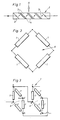
- the magnetoresistive sensor 1 shown in Fig.1 consists of a core 2 of insulating material to which has been applied a thin layer 3 of an alloy, preferably an iron-nickel alloy with approx. 20% by weight of iron and 80% by weight of nickel.
- the electric resistance of a thin layer of a ferromagnetic alloy is a function of the direction of current in the layer and the direction of a magnetic field which may be constituted of the magnetic field caused by the current on passage through the metal layer and by the outer magnetic field. This effect is largely independent of the frequency and is sensitive also to weak magnetic fields. If the metal layer consists of an alloy of the abovementioned composition very stable properties are obtained over a certain temperature range and the change in resistance may be as great as 2-3%.
- a so-called Wheatstone bridge to form a detector element 6. If all the sensors 1 in the detector element 6 are equal, the bridge is in balance. If the bridge detector element 6 is subjected to an outer magnetic field, however, the sensors 1 which are affected most by the magnetic field (the direction of the magnetic field forms the greatest angle with the sensor 1) will be subject to a resistance change. The bridge detector element 6 will then become unbalanced and a voltage difference will arise between the corner points of the bridge when the two remaining corner points of the bridge are connected via a voltage source. This change in voltage is a measure for the strength of the magnetic field , and in order to allow a more accurate detection to take place, the voltage difference on the bridge is usually amplified in amplifiers before final indication, measurement or other signalling procedure takes place.
- detector elements 6 In order to be able to function in accordance with the invention several, preferably two, detector elements 6 have to be asssembled and joined to a detector device in the manner as shown in Figure 3.
- the detector device 7 which is shown in Fig.3 is built up of two detector elements 6 which in turn, in the manner mentioned earlier, are built up of four identical sensors 1 each.
- the bridges can be joined asymmetrically as shown in the Figure. The current in both bridges or detector elements goes from a to b, if it is assumed that a is coupled to a positive potential and b is earthed.
- the detector device 7 can be formed in that two detector elements 6, which are supplied commercially cast in a plastic capsule, are assembled and fixed to one another with the help of an adhesive of some kind. Naturally it is also possible to order from the manufacturer of sensors 1 and detector elements 6 a detector device 7 consisting of two bridges 6 of sensors 1 arranged at some distance from one another.
- FIG 4 is shown how a detector device 7 consisting of two detector elements arranged adjoining one another is located close to a travelling web 8 of, for example, packing material, this web 8 being a carrier of magnetic marks or markings 9.
- the detector device 7 is provided with a guiding device 10 in the form of an arm 11 with a sliding shoe or roll 12.
- the magnetic marks 9 can have an optional function and they may be constituted, for example, of marks adapted to control and guide the forwards feed of the web in register with a printed pattern applied to the web 8 or a creaseline pattern which has been applied in order to facilitate the forming through folding of the packing material.
- the forwards feed should be monitored and be in register with the print and the creaseline pattern, since otherwise the printed information on the package becomes displaced and the forming occurs along folding lines other than those intended.
- the magnetic fields from the passing magnetic markings 9 are indicated on both the detector elements 6 included in the detector device 7.
- the detector 7 is continuously exposed to strong magnetic interference fields emanating from motors, transformers and, in packing machines of the type referred to here, from induction sealing arrangements which comprise coils or inductors generating strong, high-frequency magnetic fields by means of which heat required for the sealing is generated along the sealing zones.
- the magnetic fields from the said magnetic marks 9 or markings are of a wholly different magnitude than the interference fields and are substantially weaker. In actual fact it is so that the detector device 7 has to be located quite close to the web 8 in order that the magnetic fields from the said magnetic marks 9 should be detectable.
- the reading of the magnetic fields of the said marks 9 thus is very "distance-dependent" owing to the magnetic field being weak, and this means that the indication of magnetic fields from a mark 9 shows great differences depending on whether the detector element adjoins the mark 9 or whether the detector element 6 is a few millimetres away from the web 8.
- the detector device 7 is arranged adjoining the web 8, with specially arranged guiding devices 10 consisting of an arm 11 joined to the detector device which has a sliding shoe or roll 12 adapted to slide against the web 8 continuously controlling the position of the detector device 7 in relation to the web 8.
- the detector device 7 is exposed the whole time to magnetic interference fields of both continuous and intermittent character. These interference fields of course are indicated by the detector elements 6 of the setector device 7, but owing to the magnitude of the interference field the deflection, or rather the output voltage from the two detector elements 6, will be of the same size.
- the output voltage from the two detector elements 6 can by coupled in phase opposition to one another.
- the voltage from the detector elements 6 generated by the magnetic interference fields are simultaneous and moreover of the same size if it is assumed that the detector elements 6 are identical, the voltages will cancel out each other when they are coupled in phase opposition (or are subtracted from one another) and this means that the resulting voltage from the detector device 7 becomes zero or, in any case, negligible.
- the two detector elements 6 included in the detector device 7 will indicate the magnetic field from the mark 9 differently owing to the detector elements 6 being located at unequal distance from the mark 9. Since the indications of the magnetic mark 9 too are simultaneous and coupled in phase opposition to one another, the indications from the two detector elements 6 will partly extinguish one another, but owing to the one detector element 6 (that located closest to the web 8) generating a stronger indication than the other detector element 6, the result will be a weakened, but distinct, pulse which constitutes an indication that a magnetic control mark 9 has been detected.
- FIG 5 is shown a schematic coupling of a circuit by means of which the signals generated by the detector elements 6 can be subtracted from one another and amplified.
- magnetoresistive sensors 1 are joined in a bridge circuit to the detector element 6.
- the feed points a and earth connection points b respectively of the two bridges or detector elements 6 are arranged asymmetrically in relation to one another so that the voltage over the counterconnected "output points" c, d of the bridges 6 should lie in phase opposition to one another.
- This coupling in phase-opposition as such may be done in many different ways, e.g. with a so-called inverter and the example given here should be seen as only one of several possible solutions.
- the two detector elements 6 are also designated by I and II and, as can be seen, the connections a of the detector elements are coupled to a source of current with positive potential whereas the terminals b are connected to earth potential 14.
- the connections a of the detector elements are coupled to a source of current with positive potential whereas the terminals b are connected to earth potential 14.
- a voltage ensues over the junctions c,d of the bridges and the magnitude of this voltage difference is dependent on the magnitude of the influencing magnetic field.
- the junbctions c,d on each bridge or detector element 6 (I and II) are connected to so-called operational amplifiers 19 with the help of which the voltages supplied are amplified.
- the amplified voltages are joined at the point 22 where they at least partly extinguish one another, since they are in phase opposition.
- the current delivered by the operational amplifier 19 is conducted through the resistances 20 and 21, the resistance 21 being constituted of a potentiometer. With the help of the potentiometer 21 it is possible to adjust or zero the circuit, since it is difficult to get the detector elements exactly equal.
- the output signal from the arrangement can be standardized in its magnitude and in yet a further amplifier and circuits, not shown here, the output pulse can be shaped and a shape can be given to it which is such that a safe control of e.g. the forwards advance of the web is performed when pulses from a magnetic mark 9 are generated.
Landscapes
- Physics & Mathematics (AREA)
- Engineering & Computer Science (AREA)
- General Physics & Mathematics (AREA)
- Condensed Matter Physics & Semiconductors (AREA)
- Computer Vision & Pattern Recognition (AREA)
- Theoretical Computer Science (AREA)
- Artificial Intelligence (AREA)
- Geophysics And Detection Of Objects (AREA)
- Transmission And Conversion Of Sensor Element Output (AREA)
- Measurement Of Length, Angles, Or The Like Using Electric Or Magnetic Means (AREA)
- Inspection Of Paper Currency And Valuable Securities (AREA)
- Measuring Magnetic Variables (AREA)
- Control Of Position, Course, Altitude, Or Attitude Of Moving Bodies (AREA)
Priority Applications (1)
| Application Number | Priority Date | Filing Date | Title |
|---|---|---|---|
| AT88119015T ATE87115T1 (de) | 1987-11-26 | 1988-11-15 | Vorrichtung zum erkennen eines magnetischen mediums. |
Applications Claiming Priority (2)
| Application Number | Priority Date | Filing Date | Title |
|---|---|---|---|
| SE8704704 | 1987-11-26 | ||
| SE8704704A SE459700B (sv) | 1987-11-26 | 1987-11-26 | Saett att undertrycka verkan av magnetiska stoerfaelt vid detektering av paa en baerare anbringade magnetiska maerken eller markeringar |
Publications (2)
| Publication Number | Publication Date |
|---|---|
| EP0317879A1 true EP0317879A1 (fr) | 1989-05-31 |
| EP0317879B1 EP0317879B1 (fr) | 1993-03-17 |
Family
ID=20370404
Family Applications (1)
| Application Number | Title | Priority Date | Filing Date |
|---|---|---|---|
| EP88119015A Expired - Lifetime EP0317879B1 (fr) | 1987-11-26 | 1988-11-15 | Dispositif pour détecter un marquage magnétique |
Country Status (5)
| Country | Link |
|---|---|
| EP (1) | EP0317879B1 (fr) |
| AT (1) | ATE87115T1 (fr) |
| DE (1) | DE3879397T2 (fr) |
| ES (1) | ES2039563T3 (fr) |
| SE (1) | SE459700B (fr) |
Cited By (4)
| Publication number | Priority date | Publication date | Assignee | Title |
|---|---|---|---|---|
| WO2003095198A1 (fr) * | 2002-05-10 | 2003-11-20 | Tetra Laval Holdings & Finance S.A. | Lamine d'emballage, rouleau de plissage et couche pour un lamine d'emballage |
| WO2006065631A1 (fr) * | 2004-12-16 | 2006-06-22 | Honeywell International Inc. | Circuit de sortie de millivolts utilisable avec des circuits integres programmables de compensation de detecteurs |
| WO2006093449A1 (fr) * | 2005-03-02 | 2006-09-08 | Tetra Laval Holdings & Finance S.A. | Dispositif et procede de detection de position par marquage magnetique d'un materiau d'emballage |
| JP2014502941A (ja) * | 2010-11-29 | 2014-02-06 | テトラ ラバル ホールデイングス エ フイナンス ソシエテ アノニム | 磁化可能部分を有する包装材料 |
Citations (4)
| Publication number | Priority date | Publication date | Assignee | Title |
|---|---|---|---|---|
| US3969769A (en) * | 1974-04-29 | 1976-07-13 | U.S. Philips Corporation | Magneto-resistive head |
| US4142218A (en) * | 1975-04-14 | 1979-02-27 | U.S. Philips Corporation | Magnetoresistive head |
| US4283774A (en) * | 1979-06-13 | 1981-08-11 | Burroughs Corporation | On-chip method of balancing memory detectors and balanced detectors formed thereby |
| US4603365A (en) * | 1982-03-10 | 1986-07-29 | Copal Company Limited | Magnetic detection apparatus |
-
1987
- 1987-11-26 SE SE8704704A patent/SE459700B/sv not_active IP Right Cessation
-
1988
- 1988-11-15 ES ES198888119015T patent/ES2039563T3/es not_active Expired - Lifetime
- 1988-11-15 AT AT88119015T patent/ATE87115T1/de not_active IP Right Cessation
- 1988-11-15 DE DE8888119015T patent/DE3879397T2/de not_active Expired - Fee Related
- 1988-11-15 EP EP88119015A patent/EP0317879B1/fr not_active Expired - Lifetime
Patent Citations (4)
| Publication number | Priority date | Publication date | Assignee | Title |
|---|---|---|---|---|
| US3969769A (en) * | 1974-04-29 | 1976-07-13 | U.S. Philips Corporation | Magneto-resistive head |
| US4142218A (en) * | 1975-04-14 | 1979-02-27 | U.S. Philips Corporation | Magnetoresistive head |
| US4283774A (en) * | 1979-06-13 | 1981-08-11 | Burroughs Corporation | On-chip method of balancing memory detectors and balanced detectors formed thereby |
| US4603365A (en) * | 1982-03-10 | 1986-07-29 | Copal Company Limited | Magnetic detection apparatus |
Non-Patent Citations (1)
| Title |
|---|
| IBM Technical Disclosure Bulletin Vol. 14, No. 8, January 1972, p. 2488-2489 * |
Cited By (11)
| Publication number | Priority date | Publication date | Assignee | Title |
|---|---|---|---|---|
| WO2003095198A1 (fr) * | 2002-05-10 | 2003-11-20 | Tetra Laval Holdings & Finance S.A. | Lamine d'emballage, rouleau de plissage et couche pour un lamine d'emballage |
| US7958694B2 (en) | 2002-05-10 | 2011-06-14 | Tetra Laval Holdings & Finance S.A. | Method of controlling working operation of a filling machine |
| US9248631B2 (en) | 2002-05-10 | 2016-02-02 | Tetra Laval Holdings & Finance S.A. | Method of controlling working operation of a filling machine |
| WO2006065631A1 (fr) * | 2004-12-16 | 2006-06-22 | Honeywell International Inc. | Circuit de sortie de millivolts utilisable avec des circuits integres programmables de compensation de detecteurs |
| WO2006093449A1 (fr) * | 2005-03-02 | 2006-09-08 | Tetra Laval Holdings & Finance S.A. | Dispositif et procede de detection de position par marquage magnetique d'un materiau d'emballage |
| JP2008532039A (ja) * | 2005-03-02 | 2008-08-14 | テトラ ラバル ホールデイングス エ フイナンス ソシエテ アノニム | 磁気マーキングによって包装材料の位置を検出する位置検出器および方法 |
| RU2394207C2 (ru) * | 2005-03-02 | 2010-07-10 | Тетра Лаваль Холдингз Энд Файнэнс С.А. | Устройство определения положения и способ определения положения упаковочного материала с магнитной меткой |
| CN101120229B (zh) * | 2005-03-02 | 2011-02-16 | 利乐拉瓦尔集团及财务有限公司 | 用于检测带有磁标记的包装材料位置的位置检测器及方法 |
| EP1856477A4 (fr) * | 2005-03-02 | 2012-05-30 | Tetra Laval Holdings & Finance | Dispositif et procede de detection de position par marquage magnetique d'un materiau d'emballage |
| JP2014502941A (ja) * | 2010-11-29 | 2014-02-06 | テトラ ラバル ホールデイングス エ フイナンス ソシエテ アノニム | 磁化可能部分を有する包装材料 |
| US9208422B2 (en) | 2010-11-29 | 2015-12-08 | Tetra Laval Holdings & Finance S.A. | Packaging material comprising magnetisable portions |
Also Published As
| Publication number | Publication date |
|---|---|
| SE8704704L (sv) | 1989-05-27 |
| SE8704704D0 (sv) | 1987-11-26 |
| DE3879397T2 (de) | 1993-06-24 |
| SE459700B (sv) | 1989-07-24 |
| DE3879397D1 (de) | 1993-04-22 |
| ES2039563T3 (es) | 1993-10-01 |
| ATE87115T1 (de) | 1993-04-15 |
| EP0317879B1 (fr) | 1993-03-17 |
Similar Documents
| Publication | Publication Date | Title |
|---|---|---|
| EP1856477B1 (fr) | Dispositif magnetique et procede de detection de position par marquage magnetique d'un materiau d'emballage avec compensation magnetique | |
| US5187475A (en) | Apparatus for determining the position of an object | |
| US5629619A (en) | Noncontact distance-measuring system having at least one coil and method of noncontact distance measuring operating either on the basis of eddy currents or by inductance | |
| US5610518A (en) | Method and apparatus for detecting small magnetizable particles and flaws in nonmagnetic conductors | |
| US6828779B2 (en) | Circuit for compensating for time variation of temperature in an inductive sensor | |
| JP3445362B2 (ja) | 交流電流センサ | |
| JP2846814B2 (ja) | 位置測定装置 | |
| US6040690A (en) | Electricity measurement using two conductors | |
| US7298131B2 (en) | Current sensors | |
| US4212041A (en) | Apparatus and method for removing the effect of interference magnetic fields in a magnetic transducer device for detecting information magnetically coded on a carrier | |
| JP4894040B2 (ja) | 磁気センサ | |
| US4400752A (en) | Magneto-electric transducer for a magnetic recording system and recording system comprising such a transducer | |
| EP0317879B1 (fr) | Dispositif pour détecter un marquage magnétique | |
| JPH05314313A (ja) | 磁気インク文字読取り用磁気抵抗ヘッド | |
| US4782294A (en) | Method of measuring variation in the elongation of a very long magnetizable element of small transverse dimensions, and apparatus for implementing the method | |
| JP2000055998A (ja) | 磁気センサ装置および電流センサ装置 | |
| JPS5842900B2 (ja) | 磁気情報を読取るための装置 | |
| JP2910167B2 (ja) | 搬送車の誘導方法 | |
| JPH0427512B2 (fr) | ||
| JP2663767B2 (ja) | 変態率測定方法及びその装置 | |
| EP4471446A1 (fr) | Agencement de capteur | |
| JPH03243801A (ja) | 非接触型距離計 | |
| JPS59501838A (ja) | 誘導的長さ及び角度測定装置 | |
| JP2021028596A (ja) | ゼロフラックス型磁気センサ | |
| JP4586151B2 (ja) | 紙葉類識別装置 |
Legal Events
| Date | Code | Title | Description |
|---|---|---|---|
| PUAI | Public reference made under article 153(3) epc to a published international application that has entered the european phase |
Free format text: ORIGINAL CODE: 0009012 |
|
| AK | Designated contracting states |
Kind code of ref document: A1 Designated state(s): AT BE CH DE ES FR GB IT LI NL SE |
|
| 17P | Request for examination filed |
Effective date: 19890608 |
|
| 17Q | First examination report despatched |
Effective date: 19901207 |
|
| RTI1 | Title (correction) | ||
| GRAA | (expected) grant |
Free format text: ORIGINAL CODE: 0009210 |
|
| AK | Designated contracting states |
Kind code of ref document: B1 Designated state(s): AT BE CH DE ES FR GB IT LI NL SE |
|
| ITF | It: translation for a ep patent filed | ||
| REF | Corresponds to: |
Ref document number: 87115 Country of ref document: AT Date of ref document: 19930415 Kind code of ref document: T |
|
| REF | Corresponds to: |
Ref document number: 3879397 Country of ref document: DE Date of ref document: 19930422 |
|
| ET | Fr: translation filed | ||
| REG | Reference to a national code |
Ref country code: ES Ref legal event code: FG2A Ref document number: 2039563 Country of ref document: ES Kind code of ref document: T3 |
|
| PLBE | No opposition filed within time limit |
Free format text: ORIGINAL CODE: 0009261 |
|
| STAA | Information on the status of an ep patent application or granted ep patent |
Free format text: STATUS: NO OPPOSITION FILED WITHIN TIME LIMIT |
|
| 26N | No opposition filed | ||
| EAL | Se: european patent in force in sweden |
Ref document number: 88119015.1 |
|
| PGFP | Annual fee paid to national office [announced via postgrant information from national office to epo] |
Ref country code: AT Payment date: 19981022 Year of fee payment: 11 |
|
| PGFP | Annual fee paid to national office [announced via postgrant information from national office to epo] |
Ref country code: CH Payment date: 19981027 Year of fee payment: 11 |
|
| PGFP | Annual fee paid to national office [announced via postgrant information from national office to epo] |
Ref country code: BE Payment date: 19981117 Year of fee payment: 11 |
|
| PG25 | Lapsed in a contracting state [announced via postgrant information from national office to epo] |
Ref country code: AT Free format text: LAPSE BECAUSE OF NON-PAYMENT OF DUE FEES Effective date: 19991115 |
|
| PG25 | Lapsed in a contracting state [announced via postgrant information from national office to epo] |
Ref country code: LI Free format text: LAPSE BECAUSE OF NON-PAYMENT OF DUE FEES Effective date: 19991130 Ref country code: CH Free format text: LAPSE BECAUSE OF NON-PAYMENT OF DUE FEES Effective date: 19991130 Ref country code: BE Free format text: LAPSE BECAUSE OF NON-PAYMENT OF DUE FEES Effective date: 19991130 |
|
| BERE | Be: lapsed |
Owner name: PROFOR A.B. Effective date: 19991130 |
|
| REG | Reference to a national code |
Ref country code: CH Ref legal event code: PL |
|
| PGFP | Annual fee paid to national office [announced via postgrant information from national office to epo] |
Ref country code: FR Payment date: 20001018 Year of fee payment: 13 |
|
| PGFP | Annual fee paid to national office [announced via postgrant information from national office to epo] |
Ref country code: SE Payment date: 20001019 Year of fee payment: 13 |
|
| PGFP | Annual fee paid to national office [announced via postgrant information from national office to epo] |
Ref country code: GB Payment date: 20001020 Year of fee payment: 13 |
|
| PGFP | Annual fee paid to national office [announced via postgrant information from national office to epo] |
Ref country code: NL Payment date: 20001026 Year of fee payment: 13 |
|
| PGFP | Annual fee paid to national office [announced via postgrant information from national office to epo] |
Ref country code: ES Payment date: 20001211 Year of fee payment: 13 |
|
| PG25 | Lapsed in a contracting state [announced via postgrant information from national office to epo] |
Ref country code: GB Free format text: LAPSE BECAUSE OF NON-PAYMENT OF DUE FEES Effective date: 20011115 |
|
| PG25 | Lapsed in a contracting state [announced via postgrant information from national office to epo] |
Ref country code: SE Free format text: LAPSE BECAUSE OF NON-PAYMENT OF DUE FEES Effective date: 20011116 Ref country code: ES Free format text: LAPSE BECAUSE OF NON-PAYMENT OF DUE FEES Effective date: 20011116 |
|
| REG | Reference to a national code |
Ref country code: GB Ref legal event code: IF02 |
|
| PG25 | Lapsed in a contracting state [announced via postgrant information from national office to epo] |
Ref country code: NL Free format text: LAPSE BECAUSE OF NON-PAYMENT OF DUE FEES Effective date: 20020601 |
|
| EUG | Se: european patent has lapsed |
Ref document number: 88119015.1 |
|
| PG25 | Lapsed in a contracting state [announced via postgrant information from national office to epo] |
Ref country code: FR Free format text: LAPSE BECAUSE OF NON-PAYMENT OF DUE FEES Effective date: 20020730 |
|
| NLV4 | Nl: lapsed or anulled due to non-payment of the annual fee |
Effective date: 20020601 |
|
| REG | Reference to a national code |
Ref country code: FR Ref legal event code: ST |
|
| REG | Reference to a national code |
Ref country code: FR Ref legal event code: ST |
|
| PGFP | Annual fee paid to national office [announced via postgrant information from national office to epo] |
Ref country code: DE Payment date: 20031231 Year of fee payment: 16 |
|
| REG | Reference to a national code |
Ref country code: ES Ref legal event code: FD2A Effective date: 20021213 |
|
| PG25 | Lapsed in a contracting state [announced via postgrant information from national office to epo] |
Ref country code: DE Free format text: LAPSE BECAUSE OF NON-PAYMENT OF DUE FEES Effective date: 20050601 |
|
| PG25 | Lapsed in a contracting state [announced via postgrant information from national office to epo] |
Ref country code: IT Free format text: LAPSE BECAUSE OF NON-PAYMENT OF DUE FEES;WARNING: LAPSES OF ITALIAN PATENTS WITH EFFECTIVE DATE BEFORE 2007 MAY HAVE OCCURRED AT ANY TIME BEFORE 2007. THE CORRECT EFFECTIVE DATE MAY BE DIFFERENT FROM THE ONE RECORDED. Effective date: 20051115 |