EP0317996A2 - Drucker - Google Patents
Drucker Download PDFInfo
- Publication number
- EP0317996A2 EP0317996A2 EP88119580A EP88119580A EP0317996A2 EP 0317996 A2 EP0317996 A2 EP 0317996A2 EP 88119580 A EP88119580 A EP 88119580A EP 88119580 A EP88119580 A EP 88119580A EP 0317996 A2 EP0317996 A2 EP 0317996A2
- Authority
- EP
- European Patent Office
- Prior art keywords
- font
- data
- cartridge
- printer
- address
- Prior art date
- Legal status (The legal status is an assumption and is not a legal conclusion. Google has not performed a legal analysis and makes no representation as to the accuracy of the status listed.)
- Granted
Links
Images


Classifications
-
- G—PHYSICS
- G06—COMPUTING OR CALCULATING; COUNTING
- G06K—GRAPHICAL DATA READING; PRESENTATION OF DATA; RECORD CARRIERS; HANDLING RECORD CARRIERS
- G06K15/00—Arrangements for producing a permanent visual presentation of the output data, e.g. computer output printers
- G06K15/02—Arrangements for producing a permanent visual presentation of the output data, e.g. computer output printers using printers
-
- G—PHYSICS
- G06—COMPUTING OR CALCULATING; COUNTING
- G06K—GRAPHICAL DATA READING; PRESENTATION OF DATA; RECORD CARRIERS; HANDLING RECORD CARRIERS
- G06K2215/00—Arrangements for producing a permanent visual presentation of the output data
- G06K2215/0002—Handling the output data
- G06K2215/002—Generic data access
- G06K2215/0022—Generic data access characterised by the storage means used
- G06K2215/0025—Removable memories, e.g. cartridges
Definitions
- the present invention relates to a printer, more paticularly to a method of discriminating of and using of a memory cartridge to be connected to the printer.
- a memory cartridge is described with reference to Figs. 8 through 12.
- a printer comprises a CPU 1 connected to a CPU bus 6, a programmable ROM 2 connected to the CPU bus 6, a RAM 3 for temporarily storing a received data or other necessary data and connected to the CPU bus 6, an interface (I/F) circuit 5 for receiving a data from a host unit 4 provided outside the printer, a read/development circuit 13 connected to the data bus 6 provided for increasing a throughput and enabling to directly access to a font ROM 7 or a font RAM 10 (respectively described later) without receiving instructions from the CPU 1 for reading and developing with high speed dot image data from the font ROM 7 or the font RAM 10, the font ROM 7 connected to the read/development circuit 13 for storing a resident font data provided by the printer, for example, a Ming type, a font ROM cartridge 8 connected to the read/development circuit 13 through a connector 9 for storing a down-line load font data provided by the host unit 4, for example, Italic type, the font RAM 10 connected to the read/development circuit 13 for storing there
- the read/development circuit 13 is described in detail hereafter with reference to Fig. 9.
- a bus/address control 71 is provided for accessing a font ROM 73 or a RAM (not shown).
- An address provided by the bus/address control 71 is supplied by way of a line 84 to an address counter 72 for a font ROM 73 together with a write signal 88 generated by the bus/address control 71, while an address provided by the bus/address control 71 is supplied by way of an address line 86 to an address counter 74 for a page buffer 76.
- a read/write signal 85 for a font data generated by the bus/address control 71 is supplied to the address counter 72, the font ROM 73 and a gate 89. An output of the gate 89 is supplied to the address counter 74 and the page buffer 76.
- the gate 89 is normally open.
- One output of the address counter 72 is supplied to the font ROM 73 and another output of the address counter 72 is supplied to a decoder 95.
- An output of the decoder 95 is supplied to the font ROM 73 by way of a line 26-d, and an output of the address counter 74 is supplied to the page buffer 76.
- An output of the font ROM 73 and an output of the page buffer 76 are respectively supplied to a parallel/serial converter 77 by way of a local bus 80.
- a start signal 87 is generated by the bus/address control 71 when the page buffer 76 starts to read out the data.
- the start signal 87 is supplied to the address counter 74, a 1/8 counter 78 and the parallel/serial converter 77.
- a synchronous signal 81 generated by the bus/address control 71 is the signal indicative of a block of line or an end of line for a printing data which is supplied for each block or unit of line.
- a transfer clock 82 for the printing data generated by the bus/address control 71 is supplied to the parallel/serial converter 77 and the 1/8 counter 78 output of which is supplied to the address counter 74, the page buffer 76, and the parallel/serial converter 77.
- the 1/8 counter 78 is provided for dividing the input frequency by 8 since the input of the paralle/serial converter 77 (corresponding to the local bus 80) is composed of 8 bits.
- a buffer 79 is provided for connecting the local bus 80 and the CPU bus 6, and the CPU bus 6 and the local bus 80 are not normally connected with each other.
- the buffer 79 and the gate 89 are respectively controlled by the bus/address control 71, and such control operation can be effected when the CPU 1 reads out the data on the local bus 80.
- the address of the page buffer 76 is assigned to the location at the time of outputting the data, namely, printing the character.
- a font data of a character "A" assigned to the locations indicated as 1 through 8 in Fig. 10 is stored in the font ROM 73 as shown in Fig. 11 which explains writing of the data between the font ROM 73 and the page buffer 76.
- the bus/address control 71 sets the page buffer address "nm + 4" in the address counter 74, and issues the read/write signal 85 to thereby write a data 2 of the font ROM 73 into the page buffer 76.
- "(n + 1) m + 3" is set in the address counter 74, and a data 3 of the font ROM 73 is written into the page buffer 76.
- data 4 through 8 are sequentially written in the page buffer 76.
- the bus/address control 71 issues a start signal 87 on the basis of an instruction from the CPU 1 to thereby set the address counter 74 and the 1/8 counter 78 to an initial state (the state where the address counter 74 is set to "1", the 1/8 counter 78 is reset, and the data of the address "1" of the page buffer 76 is set in the parallel/serial converter 77). Thereafter, the synchronous signal 81 and the transfer clock 82 are respectively issued by the bus/address control 71 so that the printing data is successively outputted by the transfer clock 82.
- the output of the address counter 74 increments by 1 on the basis of the output of the 1/8 counter 78.
- a data of the address.”2 ⁇ of the page buffer 76 is set in the paralle/serial converter 77 and is successively output as the printing data by the transfer clock 82.
- a value of the address "m" is the one inherent to be determined by the capability of printing to be made by the printer.
- the bus/address control 71 issues the synchronous signal showing the first of the next line of data.
- the printing data for one page is output.
- Frequencies of a read/development clock and the transfer clock can be set to several hundred nano seconds (being set to several micro seconds through several ten micro seconds when the CPU 1 directly controls the clocks), whereby such arrangement is an effective means for a dot line printer requiring for outputting the printing data with high speed.
- An operation of the read/development circuit 13 for reading and developing the data of the font RAM is same as that of the font ROM 73 as set forth above.
- the font RAM is substituted for the font RAM 73 and a write signal 90 issued by the bus/address control 71 to the font RAM is added in the arrangement of the read/development circuit 13 for the font ROM 73 in Fig. 9.
- a data from the host unit 4 is received by the I/F circuit 5 and the content of the data is analyzed by the CPU 1 which data is stored in the RAM 3.
- the CPU 1 instructs the read/development circuit 13 to execute the operation for developing and printing the data on the basis of the data stored in the RAM 3.
- the read/development circuit 13 instructed by the CPU 1 to develop and output the content of the data can access the font ROM or the font RAM without receiving the instruction from the CPU 1 and outputs the printing data with high speed.
- the font ROM cartridge or the font RAM cartridge can be connected to the read/development circuit 13 when required.
- the present invention has been made to solve the problems of the printer and provide a printer enabling to print simultaneously font types of characters extending over a plurality of memory cartridges or a variety of down line font data with low cost.
- the printer of the present invention including a plurality of font memory cartridges provided with font memories, the font memories storing therein down line load font data of characters which are not resident in the font memories incorporated in the printer but provided by a host unit outside the printer, at least one connector being connected to anyone of a plurality of font memory cartridges for outputting the down line load font data, characterized in that the printer further including a first means for forcibly reading out the font data of the characters stored in the font memory mounted on the font memory cartridge connected to one of the connectors, and a second means for discriminating kinds of the font memory cartridge connected to one of the connectors and a content of the font data of the characters stored in the font memory mounted on the font memory cartridge on the basis of the font data of characters read out from the first means.
- An embodiment of the printer of the present invention includes a font ROM cartridge 24 and a font RAM cartridge 25.
- a font ROM 7 incorporated in the printer is connected to a read/development circuit 13 connected to a bus line 6 by way of a select line 26-d and a line 27.
- a font RAM 10 incorporated in the printer is connected to the read/development circuit 13 by way of a select line 26-a and a line 28.
- Two gate circuits 22-a, 22-b are connected to the read/development circuit 13 by way of the lines 27, 28 and select lines 26-b, 26-c.
- the gate circuit 22-a is further connected to a connector 23-a for the font ROM 24 and the gate circuit 22-b is further connected to a connector 23-b for the font RAM 25.
- the signal lines in the connector 23-a comprise address lines A20 through A-0 connected to pins 1 through 21, a read (RD) signal connected to a pin 31, a write (WR) signal connected to a pin 32, an enable signal connected to a pin 30, and data lines D7 through D0 connected to pins 22 through 29.
- the data lines D7 through D0 are leveled up to a "1" level by eight resistors (34-1 through 34-8).
- a power supply (+5V) for the ROM cartridge 24 is connected to pins 33, 34 and a ground (0V) is connected to pins 35, 36.
- the arrangement of the signal lines in the connector 22-b is same as that of the connector 23-a.
- the font ROM 24 comprises a font ROM 41 and a font ROM 42 respectively connected to some of address lines A21 through A0 by way of a line 44 (varies depending on a font ROM size to be used, for example, the address lines will be seventeen, namely, A16 through A0 when it is 128K x 8 bits), and a decoder 43 connected to the address line, e.g., A17 which is located higher the address lines set forth just above namely A16 through A0.
- the decoder 43 is connected to an enable signal 30 by way of a line 45 and a read (RD) signal 31 by way of a line 46, and an output of the decoder 43 is connected to the font ROMs 41, and 42.
- the output of the font ROMs 41 and 42 are respectively connected to data lines D7 through D0 by way of a line 47. In the arrangement of the font ROM cartridge 24, the write (WR) signal is not used.
- the RAM cartridge 25 comprises RAMs 51-a, 51-b connected to addresses A21 through A0 by way of a line 55, (varies depending on a size of RAM to be used, for example, the fifteen addresses A14 through A0 are used if it is 32K x 8 bits), and a decoder 54 connected to an enable signal 30 by way of a line 58 and also to the address located higher the fifteen addresses just mentioned above.
- An output of the decoder 54 is connected to the RAMs 51-a, 51-b, and a buffer 52. Addresses assigned to the RAMs 51-a, 51-b, and a buffer 52 are located as shown in Fig. 5(b), namely, in the manner that the buffer 52 is located at the lowest position.
- the buffer 52 connected respectively to a read (RD) signal 31 by way of a line 56, and outputs of the RAMs 51-a, 51-b.
- the RAM cartridge 25 further comprises an information generation circuit 53 provided for generating one of the codes arbitrarily selected from "01HEX” through “FEHEX” for use in the font RAM cartridge. Only when the buffer 52 is selected by the decoder 54, a content of the information generation circuit 53 ("06HEX" in Fig. 5(b)) is outputted to data D7 through D0 by way of a line 59.
- the data lines D7 through D0 is connected to the input and output terminals of the RAM 51-a, and the RAM 51-b.
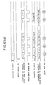
- the read/development circuit 13 forcibly generates addresses successively from the address located at the lowest in an address area asigned to the connector 23-a on the basis of the read instruction from the lowest address of the cartridge area issued by the CPU 1, so that the read data corresponding to the address is delivered to the CPU 1. Assuming that the font ROM 24 as shown in Fig. 1 is connected to the connector 23-a, the font ROM information as shown in Fig. 5(a) is delivered as the read data.
- the font ROM information means the font type, for example, a Ming (11HEX), a chinese character of JIS first standard (21HEX), or the number of characters (0DDEHEX), etc. which are all coded on the basis of the rule of the printer according to the present invention and composed of at least two codes.
- the CPU 1 can discriminate that the cartridge connected to the connector is the font ROM cartridge on the basis of the data and a content of the font. Assuming that the font RAM cartridge is connected to the connector, a cartridge information "06HEX" in "A" portion in Fig. 5(b) is successively read out as the read data so that the CPU 1 can discriminate that it is the font RAM cartridge on the basis of the data "06HEX".
- the capacity of the RAM can be also discriminated by the CPU 1, for instance, it is "06HEX : 384 K Byte RAM cartridge".
- the CPU 1 since the data lines D7 through D0 are leveled up to the "1" level by the resistors 34-1 through 34-8 as shown in Fig. 2, the read data as "FFHEX” is successively read out so that the CPU 1 can discriminate that the font ROM or font RAM cartridge is not connected to the connector. This operation is also, applicable to the connector 23-b.
- the CPU 1 can process the data received from the host unit 4 on the basis of the arrangement of the memory discriminated by the read operation mentioned above.
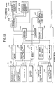
- a font ROM cartridges 101 and 103 respectively have cartridge information generation means 102, 104 (refer to Figs. 5 and 6).
- the cartridge information generation means 102 and 104 respectively connected to a cartridge information read means 106 through respectively cartridge connection means 105 (connectors).
- the cartridge information read means 106 reads out a cartridge information from the cartridge information generation means 102, 104 on the basis of an instruction of a cartridge area address arithmetic and logic means 107 and the cartridge information just read out is stored in a working register 108.
- the working register 108 is an area to store temporarily the data.
- a register address arithmetic and logic means 112 generates addresses when a register storing means 111 stores data into a register A 117, registers B-a through B-d 116, registers C-a through C-d 121, and registers Sa through Sd 118, and a register read means 113 reads out the data of the register A 117, the registers B-a through B-d 116, the registers C-a through C-d 121, and the registers Sa through Sd 118.
- a table address arithmetic and logic means 114 generates addresses when a table read means 115 reads out data of a table TA 119 and a table TB 120.
- a comparator 109 compares the data in the working register 108 with an output data from the register read means 113 and decides that both data are same or not. A result of decision is outputted to a sequence control means 110.
- the sequence control means controls sequential processes of read/decision of the cartridge information and controls to operate, when required, the cartridge area address arithmetic and logic means 112 and the table address arithmetic and logic means 114.
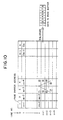
- font ROM cartridge (Ming type, JIS first standard character, 3,550 words: cartridge type data 11HEX, 21HEX, 0DHEX, DEHEX) is connected to the cartridge 1 area
- 384 K Byte RAM cartridge (cartridge type data 06HEX) is connected to the cartridge 2 area.
- a first address A1 of the cartridge 1 area (refer to Fig. 7) is outputted to the cartridge area address arithmetic and logic means 107, then in step 202, the cartridge information data D1 of the first address A1 is read out by the cartridge information read means 106.
- the data D1 is stored in the register A so that the data D1 is used to be compared with a next data to be read out.
- an address cartridge information data D2 21HEX in the address following the first address of the cartridge 1 area which has been accessed in the steps 201, 202 is read out.
- step 302 an arithmetic operation for an address of the table TB is executed by the table address arithmetic and logic means 114.
- the address of the table TB becomes "Tb + 21HEX" since 21HEX is addressed already in the working register 108.
- step 303 the content of the address of the table TB, "Tb 21HEX”, namely "JIS first standard” as the font type is read out by the table read means 115.
- the resultant read font type, namely, "JIS first standard” is stored in the register Sb by the register address arithmetic and logic means 112 and the register storing means 111.
- step 304 the data stored in the register A 117, namely, "11HEX" in step of 203 is read out by the register address arithmetic and logic means 112 and the register read means 113, then the content of the address of the table TB 120, "Tb + 11HEX", namely, "Ming type” is read out in steps of 305 and 306 in the same manner as steps of 302 and 303.
- the resultant read content, namely, "Ming type” is stored in the register Sa.
- step 307 the cartridge information of the next address (0DHEX) following the address of the cartridge 1 area accessed in step of 204 is read out, and the content thereof is stored in the register Sc in step 308.
- the cartridge information of the next address (DEHEX) is stored in the register Sd in steps 309 and 310.
- the execution of the subroutine process will be completed in the steps described above.
- a next step is returned to the step 208 in the processes as shown in Fig. 14.
- step 208 the content of the registers Sa through Sd stored in step 207 of the subroutine process is transferred to the registers Ba through Bd on the ground that the registers Sa through Sd are common registers used in each subroutine process.
- the cartridge 1 area is thus decided.
- the cartridge information data D3 and D4 of the cartridge 2 are read out in steps 209 through 212 in the same manner as steps 201 through 205.
- step 207 a subroutine process for decision of the font type is executed in step 207.
- step 401 the data (06HEX) stored in step 211 is read out by step 401, and subjected to the operations by steps 402 and 403 in the same manner as steps of 305 and 306. Then, the cartridge font type data "384 K Byte RAM cartridge" is read out of the table Ta which is stored in the register Sa.
- the data "00HEX" is stored in the registers Sb through Sd by step 404.
- This storage operation is made as a complemental process for keeping the content of the registers Sb through Sd unstable although only the data of the register Sa is enough to be stored since the RAM cartridge information is composed of a capacity thereof.
- step 214 Upon the completion of the decision of the cartridge 2 area, the step is returned to step 214 in Fig. 14.
- step 214 the contents of the registers Sa through Sd are transferred to the registers C-a through C-d in the same manner of step 208.
- the contents of the registers 2-a through 2-d are only substituted by the contents of the registers 3-a through 3-d upon execution of a series of processes set forth above.
- a connector for a plurality of cartridge memories can be arbitrarily connected to a font ROM cartridge or a font RAM cartridge so that it becomes possible to provide a printer enabling to print simultaneously font types of characters extending over a plurality of memory cartridges or a variety of down-line load font data with low cost.
- the shapes of the cartridges can be uniform so that cases and connectors can be obtained by a mass production.
- the present invention is not limited to a high speed printer having read/development circuit set forth above but can be employed by a low speed printer having no read/development circuit but elements controlled by the CPU.
- the present invention is also applicable to various printers employing any kind of printing method such as wire dot printer, a thermal printer, an inject-type printer, a facsimile printer, an electrostatic printer, etc.
Landscapes
- Engineering & Computer Science (AREA)
- General Engineering & Computer Science (AREA)
- Physics & Mathematics (AREA)
- General Physics & Mathematics (AREA)
- Theoretical Computer Science (AREA)
- Record Information Processing For Printing (AREA)
- Dot-Matrix Printers And Others (AREA)
- Storing Facsimile Image Data (AREA)
Applications Claiming Priority (2)
| Application Number | Priority Date | Filing Date | Title |
|---|---|---|---|
| JP62295099A JPH01136770A (ja) | 1987-11-25 | 1987-11-25 | プリンタ |
| JP295099/87 | 1987-11-25 |
Publications (3)
| Publication Number | Publication Date |
|---|---|
| EP0317996A2 true EP0317996A2 (de) | 1989-05-31 |
| EP0317996A3 EP0317996A3 (de) | 1991-09-18 |
| EP0317996B1 EP0317996B1 (de) | 1995-03-15 |
Family
ID=17816287
Family Applications (1)
| Application Number | Title | Priority Date | Filing Date |
|---|---|---|---|
| EP19880119580 Expired - Lifetime EP0317996B1 (de) | 1987-11-25 | 1988-11-24 | Drucker |
Country Status (3)
| Country | Link |
|---|---|
| EP (1) | EP0317996B1 (de) |
| JP (1) | JPH01136770A (de) |
| DE (1) | DE3853339T2 (de) |
Cited By (7)
| Publication number | Priority date | Publication date | Assignee | Title |
|---|---|---|---|---|
| EP0356076A3 (en) * | 1988-08-19 | 1990-12-27 | Canon Kabushiki Kaisha | Pattern output apparatus |
| EP0387039A3 (de) * | 1989-03-08 | 1991-03-06 | Canon Kabushiki Kaisha | Ausgabevorrichtung |
| FR2662833A1 (fr) * | 1990-05-31 | 1991-12-06 | Toshiba Kk | Appareil de traitement de donnees effectuant une operation de formation d'image. |
| EP0375086A3 (de) * | 1988-12-19 | 1992-03-18 | MANNESMANN Aktiengesellschaft | Verfahren zum Programmieren und zur Auswahl von Funktionen eines Computer-Peripheriegerätes, insbesondere eines Druckers |
| EP0481518A3 (en) * | 1990-10-19 | 1993-04-14 | Oki Electric Industry Company, Limited | Printer provided with power font memory card |
| EP0478357A3 (en) * | 1990-09-28 | 1993-09-15 | Xerox Corporation | Font storage management and control arrangement |
| EP0580321A1 (de) * | 1992-07-24 | 1994-01-26 | Esselte Dymo N.V. | Druckvorrichtung |
Families Citing this family (2)
| Publication number | Priority date | Publication date | Assignee | Title |
|---|---|---|---|---|
| KR930011662B1 (ko) * | 1990-11-30 | 1993-12-16 | 현대전자산업 주식회사 | 카트리지를 이용한 lbp 시스팀 |
| JP2008057756A (ja) | 2006-09-04 | 2008-03-13 | Kayaba Ind Co Ltd | 往復動用オイルシール |
Family Cites Families (2)
| Publication number | Priority date | Publication date | Assignee | Title |
|---|---|---|---|---|
| JPS6158749A (ja) * | 1984-08-31 | 1986-03-26 | Toshiba Corp | 印字処理装置 |
| JPS61225075A (ja) * | 1985-03-30 | 1986-10-06 | Toshiba Corp | 印字装置 |
-
1987
- 1987-11-25 JP JP62295099A patent/JPH01136770A/ja active Pending
-
1988
- 1988-11-24 EP EP19880119580 patent/EP0317996B1/de not_active Expired - Lifetime
- 1988-11-24 DE DE19883853339 patent/DE3853339T2/de not_active Expired - Fee Related
Cited By (12)
| Publication number | Priority date | Publication date | Assignee | Title |
|---|---|---|---|---|
| EP0356076A3 (en) * | 1988-08-19 | 1990-12-27 | Canon Kabushiki Kaisha | Pattern output apparatus |
| US5675722A (en) * | 1988-08-19 | 1997-10-07 | Canon Kabushiki Kaisha | Pattern output apparatus |
| EP0375086A3 (de) * | 1988-12-19 | 1992-03-18 | MANNESMANN Aktiengesellschaft | Verfahren zum Programmieren und zur Auswahl von Funktionen eines Computer-Peripheriegerätes, insbesondere eines Druckers |
| EP0387039A3 (de) * | 1989-03-08 | 1991-03-06 | Canon Kabushiki Kaisha | Ausgabevorrichtung |
| EP0618547A3 (de) * | 1989-03-08 | 1994-12-14 | Canon Kk | Ausgabevorrichtung. |
| US5696984A (en) * | 1989-03-08 | 1997-12-09 | Canon Kabushiki Kaisha | Output apparatus and method for varying size of cache memory area |
| FR2662833A1 (fr) * | 1990-05-31 | 1991-12-06 | Toshiba Kk | Appareil de traitement de donnees effectuant une operation de formation d'image. |
| US5394514A (en) * | 1990-05-31 | 1995-02-28 | Kabushiki Kaisha Toshiba | Image forming apparatus having detachably installed bit image forming unit |
| EP0478357A3 (en) * | 1990-09-28 | 1993-09-15 | Xerox Corporation | Font storage management and control arrangement |
| EP0481518A3 (en) * | 1990-10-19 | 1993-04-14 | Oki Electric Industry Company, Limited | Printer provided with power font memory card |
| EP0580321A1 (de) * | 1992-07-24 | 1994-01-26 | Esselte Dymo N.V. | Druckvorrichtung |
| US5700098A (en) * | 1992-07-24 | 1997-12-23 | Esselte N.V. | Printing device |
Also Published As
| Publication number | Publication date |
|---|---|
| EP0317996A3 (de) | 1991-09-18 |
| DE3853339D1 (de) | 1995-04-20 |
| DE3853339T2 (de) | 1995-07-27 |
| JPH01136770A (ja) | 1989-05-30 |
| EP0317996B1 (de) | 1995-03-15 |
Similar Documents
| Publication | Publication Date | Title |
|---|---|---|
| CA1042354A (en) | Printer | |
| US4660999A (en) | Dot-matrix printer with font cartridge unit | |
| EP0481518B1 (de) | Drucker mit Typensatz-Speicherkarte | |
| US5051925A (en) | Printer for converting character codes into bit images | |
| CA1044607A (en) | Intermixed line heights and blank line formation in a buffered printer | |
| US4466123A (en) | Apparatus and method for correcting contour line pattern images | |
| EP0317996B1 (de) | Drucker | |
| US5272768A (en) | Blank strip font compression method and device, and resulting stored, decompressible font | |
| EP0357383B1 (de) | Ausgabegerät | |
| US5029109A (en) | Image forming device with a small sized memory device employing a bit map assignment system | |
| EP0395916A2 (de) | Bildanzeigesystem mit getrenntem Schriftsatz und Bilddarstellungs-Attributen | |
| US20030193691A1 (en) | Recording apparatus and method for controlling recording apparatus | |
| US4703438A (en) | Character signal generator | |
| US5360277A (en) | Label printer with selective memory update | |
| EP0629973B1 (de) | Ausgabevorrichtung und -verfahren | |
| US6449665B1 (en) | Means for reducing direct memory access | |
| US5963713A (en) | Printer using direct memory access and refreshing | |
| EP0424885B1 (de) | Steuervorrichtung für Drucker mit hoher Geschwindigkeit und Qualität | |
| US5345314A (en) | Laser beam printing system utilizing a plurality of cartridges | |
| JP3666888B2 (ja) | カラー処理装置およびその方法 | |
| US4490058A (en) | Line printer and type carrier for use therein | |
| EP0072708A2 (de) | Drucker | |
| JP3018692B2 (ja) | 印字装置 | |
| JPS61193864A (ja) | ドツトプリンタ制御方式 | |
| JP2740197B2 (ja) | ビットマップ描画装置 |
Legal Events
| Date | Code | Title | Description |
|---|---|---|---|
| PUAI | Public reference made under article 153(3) epc to a published international application that has entered the european phase |
Free format text: ORIGINAL CODE: 0009012 |
|
| AK | Designated contracting states |
Kind code of ref document: A2 Designated state(s): DE FR GB |
|
| PUAL | Search report despatched |
Free format text: ORIGINAL CODE: 0009013 |
|
| AK | Designated contracting states |
Kind code of ref document: A3 Designated state(s): DE FR GB |
|
| RHK1 | Main classification (correction) |
Ipc: G06K 15/02 |
|
| 17P | Request for examination filed |
Effective date: 19920320 |
|
| R17P | Request for examination filed (corrected) |
Effective date: 19920424 |
|
| 17Q | First examination report despatched |
Effective date: 19930105 |
|
| GRAA | (expected) grant |
Free format text: ORIGINAL CODE: 0009210 |
|
| AK | Designated contracting states |
Kind code of ref document: B1 Designated state(s): DE FR GB |
|
| REF | Corresponds to: |
Ref document number: 3853339 Country of ref document: DE Date of ref document: 19950420 |
|
| ET | Fr: translation filed | ||
| PLBE | No opposition filed within time limit |
Free format text: ORIGINAL CODE: 0009261 |
|
| STAA | Information on the status of an ep patent application or granted ep patent |
Free format text: STATUS: NO OPPOSITION FILED WITHIN TIME LIMIT |
|
| 26N | No opposition filed | ||
| PGFP | Annual fee paid to national office [announced via postgrant information from national office to epo] |
Ref country code: FR Payment date: 19981110 Year of fee payment: 11 |
|
| PGFP | Annual fee paid to national office [announced via postgrant information from national office to epo] |
Ref country code: GB Payment date: 19981127 Year of fee payment: 11 |
|
| PGFP | Annual fee paid to national office [announced via postgrant information from national office to epo] |
Ref country code: DE Payment date: 19981130 Year of fee payment: 11 |
|
| PG25 | Lapsed in a contracting state [announced via postgrant information from national office to epo] |
Ref country code: GB Free format text: LAPSE BECAUSE OF NON-PAYMENT OF DUE FEES Effective date: 19991124 |
|
| GBPC | Gb: european patent ceased through non-payment of renewal fee |
Effective date: 19991124 |
|
| PG25 | Lapsed in a contracting state [announced via postgrant information from national office to epo] |
Ref country code: FR Free format text: LAPSE BECAUSE OF NON-PAYMENT OF DUE FEES Effective date: 20000731 |
|
| PG25 | Lapsed in a contracting state [announced via postgrant information from national office to epo] |
Ref country code: DE Free format text: LAPSE BECAUSE OF NON-PAYMENT OF DUE FEES Effective date: 20000901 |
|
| REG | Reference to a national code |
Ref country code: FR Ref legal event code: ST |