EP0318011B1 - Semiconductor memory device with discharging circuit - Google Patents
Semiconductor memory device with discharging circuit Download PDFInfo
- Publication number
- EP0318011B1 EP0318011B1 EP19880119609 EP88119609A EP0318011B1 EP 0318011 B1 EP0318011 B1 EP 0318011B1 EP 19880119609 EP19880119609 EP 19880119609 EP 88119609 A EP88119609 A EP 88119609A EP 0318011 B1 EP0318011 B1 EP 0318011B1
- Authority
- EP
- European Patent Office
- Prior art keywords
- field effect
- type field
- channel type
- effect transistors
- bit lines
- Prior art date
- Legal status (The legal status is an assumption and is not a legal conclusion. Google has not performed a legal analysis and makes no representation as to the accuracy of the status listed.)
- Expired - Lifetime
Links
- 239000004065 semiconductor Substances 0.000 title claims description 18
- 238000007599 discharging Methods 0.000 title claims description 11
- 230000005669 field effect Effects 0.000 claims description 38
- 230000001902 propagating effect Effects 0.000 claims description 3
- 239000000758 substrate Substances 0.000 claims description 3
- 230000003071 parasitic effect Effects 0.000 description 4
- 238000010586 diagram Methods 0.000 description 3
- 230000008878 coupling Effects 0.000 description 1
- 238000010168 coupling process Methods 0.000 description 1
- 238000005859 coupling reaction Methods 0.000 description 1
- 229910021419 crystalline silicon Inorganic materials 0.000 description 1
- 230000003247 decreasing effect Effects 0.000 description 1
- 230000008030 elimination Effects 0.000 description 1
- 238000003379 elimination reaction Methods 0.000 description 1
- 230000010354 integration Effects 0.000 description 1
Images

Classifications
-
- G—PHYSICS
- G11—INFORMATION STORAGE
- G11C—STATIC STORES
- G11C7/00—Arrangements for writing information into, or reading information out from, a digital store
- G11C7/12—Bit line control circuits, e.g. drivers, boosters, pull-up circuits, pull-down circuits, precharging circuits, equalising circuits, for bit lines
Definitions
- This invention relates to a semiconductor memory device and, more particularly, to a discharging circuit provided in association with the bit lines for coupling unselected bit lines to the ground.
- a semiconductor memory device comprises a plurality of memory cells arranged in rows and columns and respectively storing data bits, a plurality of bit lines each provided in association with the memory cells in each column, a plurality of word lines each coupled to the memory cells in each row for causing the memory cells to supply the bit lines with the data bits stored therein, a column selector circuit for propagating one of the data bits, and a output circuit for the data bit transferred from the column selector circuit.
- one of the word lines is activated for causing the memory cells coupled thereto to supply the bit lines with the data bits, respectively, and the column selector circuit allows one of the data bits to be latched in the output circuit. Then, the data bit is supplied from the output circuit to a destination such as a micro-processor.
- the present invention proposes to couple the unselected bit lines to the ground.
- a semiconductor memory device fabricated on a semiconductor substrate, comprising: a) a plurality of memory cells arranged in rows and columns and capable of storing data bits; b) a plurality of bit lines respectively coupled to the columns of memory cells for propagating the data bits read out from memory cells each selected from each column; c) a plurality of word lines respectively coupled to the rows of memory cells and selecting a row of memory cells for supplying the data bits to the bit lines; d) a row address decoder circuit operative to activate one of the word lines; e) a column address decoder circuit operative to produce a bit line selecting signal for specifying one of the bit lines, the bit line selecting signal having a plurality of bits; f) an output circuit operative to latch one of the data bits on said one of said bit lines; g) a column selector circuit responsive to the bit line selecting signal and operative to transfer the one of the data bits from the associated bit line to the output circuit; and h) a dischar
- Fig. 2 of the drawings there is shown a part of the circuit arrangement of a semiconductor memory device embodying the present invention.
- the semiconductor memory device illustrated in Fig. 2 is fabricated on a semiconductor substrate 11 of, for example, single crystalline silicon and largely comprises a memory cell array 12, a row address decoder circuit 13, a column address decoder circuit 14, a column selector circuit 15, an output buffer circuit 16, and a discharging circuit 17.
- the memory cell array 12 has a plurality of memory cells arranged in rows and columns, but the memory cells 18 to 27 in parts of the two rows are shown in the figure.
- the memory cells in each row are coupled to each of word lines W1 to Wn, and the row address decoder circuit 13 activates one of the word lines W1 to Wn on the basis of a row address signal supplied from the outside thereof.
- the memory cells in each column are coupled to each of bit lines 28 to 33 which in turn are coupled to the column selector circuit 15.
- the column selector circuit 15 is provided with a plurality of stages including the first stage 34, and each of the stages have n-channel type field effect transistors provided in association with the bit lines 28 to 33, respectively, and an inverter circuit.
- the first stage 34 has n-channel type field effect transistors 36 to 40a coupled to the bit lines 28 to 33, respectively.
- the column address decoder circuit 14 has a plurality of control lines equal in number to the stages of the column selector circuit 15, and a multi-bit bit line selecting signal BL is supplied to the control lines.
- Each of the control lines is associated with each of the stages and coupled directly to the gate electrodes of a half of the n-channel type field effect transistors and the inverter circuit 35 which is coupled to the gate electrodes of the other half of the n-channel type field effect transistors.
- the n-channel type field effect transistors coupled at the gate electrodes to the inverter circuit are arranged to be located on both sides of each n-channel type field effect transistor directly coupled to the control line.
- one of the control line is coupled to the gate electrodes of the n-channel type field effect transistors 36, 38 and 40, but the inverter circuit 35 is coupled to the gate electrodes of the n-channel type field effect transistors 37, 39 and 40a.
- Each of the stages thus arranged is operative to transfer a half of the data bits supplied thereto to the subsequent stage, so that only one of the data bits is supplied from the final stage of the column selector circuit 15 to the output buffer circuit 16.
- the discharging circuit 17 has a plurality of n-channel type field effect transistors equal in number to the bit lines, so that the n-channel type field effect transistors 41 to 46 are coupled to the bit lines 28 to 33, respectively.
- the n-channel type field effect transistors 42, 44 and 46 are directly coupled to the gate electrodes of the n-channel type field effect transistors 42, 44 and 46, but the n-channel type field effect transistors 41, 43 and 45 are coupled at the gate electrodes thereof to the inverter circuit 35. All of the n-channel type field effect transistors 41 to 46 are coupled at the other ends thereof to a ground terminal.
- the n-channel type field effect transistors 41, 43 and 45 gated by the inverter circuit 35 are provided in association with the bit lines 28, 30 and 32 which in turn are provided in association with the n-channel type field effect transistors 36, 38 and 40.
- the n-channel type field effect transistors 42, 44 and 46 gated by the control line are provided in association with the bit lines 29, 31 and 33, and the n-channel type field effect transistors 37, 39 and 40a are provided in association with the inverter circuit 35.
- the n-channel type field effect transistors 41 to 46 corresponds to the n-channel type field effect transistors 36 to 41 in view of the bit lines 28 to 33, and the n-channel type field effect transistors 41 to 46 are complementarily shifted between the on-states and the off-states with respect to the n-channel type field effect transistors 36 to 40a.
- the row address decoder circuit 13 shifts the word line W1 to the active high voltage level, and the column address decoder circuit 14 produces the multi-bit bit line selecting signal BL which has a bit of the low voltage level supplied to the control line provided in association with the first stage 34.
- the word line W1 goes up to the active high voltage level
- the data bits are supplied from the memory cells 18 to 22 to the bit lines 28 to 32, respectively.
- the n-channel type field effect transistors 36, 38 and 40 are turned off, so that data bits on the bit lines 28, 30 and 32 are blocked by the n-channel type field effect transistors 36, 38 and 40.
- the n-channel type field effect transistors 37 and 39 turn on to transfer the data bits on the bit lines 29 and 31 to the subsequent stage.
- the data bit on the bit line 29 is finally transferred to the output buffer circuit 16.
- the n-channel type field effect transistors 42, 44 and 46 remain off, however, the inverse of the bit is supplied from the inverter circuit 35 to the n-channel type field effect transistors 41, 43 and 45, so that the bit lines 28, 30 and 32 are grounded.
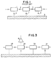
- the bit line 29 coupled to the accessed memory cell 19 is neighbored by the bit lines 28 and 30 coupled to the ground terminal as illustrated in Fig. 3.
- the total parasitic capacitance coupled to the bit line 29 is drastically reduced due to the elimination of capacitances each produced between the adjacent bit lines. Then, no fluctuation takes place in the voltage level on the bit line 29, and, for this reason, the data bit read out from the memory cell 19 is correctly transferred to the output circuit 16.
Landscapes
- Static Random-Access Memory (AREA)
- Dram (AREA)
Applications Claiming Priority (2)
| Application Number | Priority Date | Filing Date | Title |
|---|---|---|---|
| JP300609/87 | 1987-11-27 | ||
| JP62300609A JPH01140496A (ja) | 1987-11-27 | 1987-11-27 | 半導体記憶装置 |
Publications (3)
| Publication Number | Publication Date |
|---|---|
| EP0318011A2 EP0318011A2 (en) | 1989-05-31 |
| EP0318011A3 EP0318011A3 (en) | 1991-03-06 |
| EP0318011B1 true EP0318011B1 (en) | 1994-01-19 |
Family
ID=17886911
Family Applications (1)
| Application Number | Title | Priority Date | Filing Date |
|---|---|---|---|
| EP19880119609 Expired - Lifetime EP0318011B1 (en) | 1987-11-27 | 1988-11-24 | Semiconductor memory device with discharging circuit |
Country Status (3)
| Country | Link |
|---|---|
| EP (1) | EP0318011B1 (ja) |
| JP (1) | JPH01140496A (ja) |
| DE (1) | DE3887289D1 (ja) |
Families Citing this family (4)
| Publication number | Priority date | Publication date | Assignee | Title |
|---|---|---|---|---|
| JPH0426989A (ja) * | 1990-05-18 | 1992-01-30 | Toshiba Corp | ダイナミックメモリ装置 |
| JP3210355B2 (ja) * | 1991-03-04 | 2001-09-17 | 株式会社東芝 | 不揮発性半導体記憶装置 |
| FR2881565B1 (fr) * | 2005-02-03 | 2007-08-24 | Atmel Corp | Circuits de selection de ligne binaire pour memoires non volatiles |
| US8179708B2 (en) | 2009-02-18 | 2012-05-15 | Atmel Corporation | Anti-cross-talk circuitry for ROM arrays |
Family Cites Families (2)
| Publication number | Priority date | Publication date | Assignee | Title |
|---|---|---|---|---|
| US3699537A (en) * | 1969-05-16 | 1972-10-17 | Shell Oil Co | Single-rail mosfet memory with capacitive storage |
| US3765002A (en) * | 1971-04-20 | 1973-10-09 | Siemens Ag | Accelerated bit-line discharge of a mosfet memory |
-
1987
- 1987-11-27 JP JP62300609A patent/JPH01140496A/ja active Pending
-
1988
- 1988-11-24 DE DE88119609T patent/DE3887289D1/de not_active Expired - Lifetime
- 1988-11-24 EP EP19880119609 patent/EP0318011B1/en not_active Expired - Lifetime
Also Published As
| Publication number | Publication date |
|---|---|
| DE3887289D1 (de) | 1994-03-03 |
| EP0318011A2 (en) | 1989-05-31 |
| JPH01140496A (ja) | 1989-06-01 |
| EP0318011A3 (en) | 1991-03-06 |
Similar Documents
| Publication | Publication Date | Title |
|---|---|---|
| EP0300467B1 (en) | Semiconductur memory device with redundant memory cell array | |
| US4485460A (en) | ROM coupling reduction circuitry | |
| EP0165106A2 (en) | Semiconductor memory device | |
| US5406516A (en) | Semiconductor memory device | |
| EP0142127A2 (en) | Redundancy circuit for a semiconductor memory device | |
| US4086662A (en) | Memory system with read/write control lines | |
| US5299161A (en) | Method and device for improving performance of a parallel write test of a semiconductor memory device | |
| US6515915B2 (en) | Circuits and methods for outputting multi-level data through a single input/output pin | |
| EP0264929A2 (en) | Semiconductor memory device with improved bit line arrangement | |
| US6178134B1 (en) | Static random access memory with global bit-lines | |
| JP2573380B2 (ja) | 不揮発性半導体メモリ | |
| EP0454061B1 (en) | Dynamic random access memory device with improved power supply system for speed-up of rewriting operation on data bits read-out from memory cells | |
| KR100470971B1 (ko) | 리드 전용 메모리 셀, 이 셀의 프로그램 방법, 이 셀의레이아웃 방법, 및 이 셀을 구비한 리드 전용 메모리 장치 | |
| US5414657A (en) | Asynchronous static random access memory device for propagating read-out data bit through single bit line | |
| US5099452A (en) | Semiconductor memory including reduced capacitive coupling between adjacent bit lines | |
| US20030012047A1 (en) | Mid array isolate ciucuit layout | |
| US8077494B2 (en) | Ferroelectric memory with sub bit-lines connected to each other and to fixed potentials | |
| US6717867B2 (en) | SRAM power-up system and method | |
| EP0318011A2 (en) | Semiconductor memory device with discharging circuit | |
| EP0404013A2 (en) | Semiconductor memory device with an improved write control circuit | |
| US5383158A (en) | Semiconductor memory device equipped with discharging unit for bit lines accessed with invalid address | |
| EP0329182B1 (en) | Decoder buffer circuit incorporated in semiconductor memory device | |
| JPH0581895A (ja) | メモリ装置 | |
| US4875194A (en) | Semiconductor memory device with protection cells | |
| US5828618A (en) | Line memory |
Legal Events
| Date | Code | Title | Description |
|---|---|---|---|
| PUAI | Public reference made under article 153(3) epc to a published international application that has entered the european phase |
Free format text: ORIGINAL CODE: 0009012 |
|
| 17P | Request for examination filed |
Effective date: 19881124 |
|
| AK | Designated contracting states |
Kind code of ref document: A2 Designated state(s): DE FR GB |
|
| PUAL | Search report despatched |
Free format text: ORIGINAL CODE: 0009013 |
|
| AK | Designated contracting states |
Kind code of ref document: A3 Designated state(s): DE FR GB |
|
| 17Q | First examination report despatched |
Effective date: 19920728 |
|
| GRAA | (expected) grant |
Free format text: ORIGINAL CODE: 0009210 |
|
| AK | Designated contracting states |
Kind code of ref document: B1 Designated state(s): DE FR GB |
|
| PG25 | Lapsed in a contracting state [announced via postgrant information from national office to epo] |
Ref country code: DE Effective date: 19940119 Ref country code: FR Effective date: 19940119 |
|
| REF | Corresponds to: |
Ref document number: 3887289 Country of ref document: DE Date of ref document: 19940303 |
|
| EN | Fr: translation not filed | ||
| PLBE | No opposition filed within time limit |
Free format text: ORIGINAL CODE: 0009261 |
|
| STAA | Information on the status of an ep patent application or granted ep patent |
Free format text: STATUS: NO OPPOSITION FILED WITHIN TIME LIMIT |
|
| 26N | No opposition filed | ||
| REG | Reference to a national code |
Ref country code: GB Ref legal event code: IF02 |
|
| REG | Reference to a national code |
Ref country code: GB Ref legal event code: 732E |
|
| REG | Reference to a national code |
Ref country code: GB Ref legal event code: 732E |
|
| PGFP | Annual fee paid to national office [announced via postgrant information from national office to epo] |
Ref country code: GB Payment date: 20071121 Year of fee payment: 20 |
|
| REG | Reference to a national code |
Ref country code: GB Ref legal event code: PE20 Expiry date: 20081123 |
|
| PG25 | Lapsed in a contracting state [announced via postgrant information from national office to epo] |
Ref country code: GB Free format text: LAPSE BECAUSE OF EXPIRATION OF PROTECTION Effective date: 20081123 |