EP0318274A2 - Verfahren und Vorrichtung zur Fehlerdetektierung und -diskriminierung in Energieübertragungsnetzen - Google Patents
Verfahren und Vorrichtung zur Fehlerdetektierung und -diskriminierung in Energieübertragungsnetzen Download PDFInfo
- Publication number
- EP0318274A2 EP0318274A2 EP19880311098 EP88311098A EP0318274A2 EP 0318274 A2 EP0318274 A2 EP 0318274A2 EP 19880311098 EP19880311098 EP 19880311098 EP 88311098 A EP88311098 A EP 88311098A EP 0318274 A2 EP0318274 A2 EP 0318274A2
- Authority
- EP
- European Patent Office
- Prior art keywords
- circuit
- signals
- coupled
- discriminating
- discriminating means
- Prior art date
- Legal status (The legal status is an assumption and is not a legal conclusion. Google has not performed a legal analysis and makes no representation as to the accuracy of the status listed.)
- Granted
Links
- 230000005540 biological transmission Effects 0.000 title claims abstract description 69
- 238000000034 method Methods 0.000 title claims description 25
- 239000008186 active pharmaceutical agent Substances 0.000 claims abstract description 28
- 230000002441 reversible effect Effects 0.000 claims abstract description 16
- 230000004044 response Effects 0.000 claims description 16
- 230000008878 coupling Effects 0.000 claims description 7
- 238000010168 coupling process Methods 0.000 claims description 7
- 238000005859 coupling reaction Methods 0.000 claims description 7
- 238000002955 isolation Methods 0.000 claims description 4
- 230000001143 conditioned effect Effects 0.000 claims description 3
- 238000004891 communication Methods 0.000 abstract description 8
- 230000008901 benefit Effects 0.000 abstract description 2
- 239000003990 capacitor Substances 0.000 description 17
- 238000011144 upstream manufacturing Methods 0.000 description 9
- 230000002238 attenuated effect Effects 0.000 description 7
- 208000036552 dowling-degos disease 3 Diseases 0.000 description 7
- 238000012544 monitoring process Methods 0.000 description 3
- 238000012546 transfer Methods 0.000 description 3
- 230000008859 change Effects 0.000 description 2
- 238000004519 manufacturing process Methods 0.000 description 2
- 230000035945 sensitivity Effects 0.000 description 2
- 238000013459 approach Methods 0.000 description 1
- 239000004020 conductor Substances 0.000 description 1
- 238000009795 derivation Methods 0.000 description 1
- 238000001514 detection method Methods 0.000 description 1
- 238000007599 discharging Methods 0.000 description 1
- 239000011810 insulating material Substances 0.000 description 1
- 238000012986 modification Methods 0.000 description 1
- 230000004048 modification Effects 0.000 description 1
- 230000000737 periodic effect Effects 0.000 description 1
- 230000002085 persistent effect Effects 0.000 description 1
- 230000000750 progressive effect Effects 0.000 description 1
- 230000011664 signaling Effects 0.000 description 1
Images


Classifications
-
- H—ELECTRICITY
- H02—GENERATION; CONVERSION OR DISTRIBUTION OF ELECTRIC POWER
- H02H—EMERGENCY PROTECTIVE CIRCUIT ARRANGEMENTS
- H02H1/00—Details of emergency protective circuit arrangements
- H02H1/0007—Details of emergency protective circuit arrangements concerning the detecting means
- H02H1/0015—Using arc detectors
-
- H—ELECTRICITY
- H02—GENERATION; CONVERSION OR DISTRIBUTION OF ELECTRIC POWER
- H02H—EMERGENCY PROTECTIVE CIRCUIT ARRANGEMENTS
- H02H7/00—Emergency protective circuit arrangements specially adapted for specific types of electric machines or apparatus or for sectionalised protection of cable or line systems, and effecting automatic switching in the event of an undesired change from normal working conditions
- H02H7/26—Sectionalised protection of cable or line systems, e.g. for disconnecting a section on which a short-circuit, earth fault, or arc discharge has occured
Definitions
- the present invention relates to a method and apparatus for detecting and discriminating faults in transmission circuits.
- EHV extremely high voltage
- a unit type protection system in which monitoring equipment with an associated circuit breaker is provided at each end of a transmission line.
- a communication channel is provided to link the monitoring equipment at each end of the line such that the circuit breakers are tripped by information derived from more than one location.
- This system therefore, has a high inherent capacity to discriminate between fault conditions, and in particular to distinguish between faults internal to the line, which require its isolation, and faults in neighbouring lines, which do not require the subject line to be shut-down.
- the communication equipment itself needs to be reliable and secure, and it is therefore expensive to provide and to install. Furthermore, careful monitoring of the communication equipment itself is additionally required.
- a method of detecting and discriminating faults in a transmission circuit to which a discriminating means is coupled for receiving signals from said circuit comprising detecting the existence of signals in the circuit having a frequency within a predetermined frequency range, generating one or more locative signals in response to a fault, said discriminating means being responsive to signals within the predetermined frequency range and to said locative signals, and causing said discriminating means to output a fault signal only when said discriminating means receives one or more selected locative signals within a time period in which the existence of signals within said predetermined frequency range is detected.
- the present invention utilises the high frequency noise invariably generated by a fault to aid in the discrimination of faults. It is well known that faults produce wideband noise, but previously this noise has been considered as a nuisance, and even a problem, because it can interfere with the communications by the previously necessary communication equipment.
- the invention also extends to a method of protecting a transmission system against faults, the transmission system including one or more transmission circuits, respective discriminating means being coupled to each end of each circuit for receiving signals therefrom, the method comprising the steps of detecting the existence of signals in each transmission circuit having a frequency within a predetermined frequency range, generating one or more locative signals in response to the occurrence of a fault, each discriminating means being responsive to signals, within the predetermined frequency range and to locative signals, and causing each discriminating means to output a fault signal only when said discriminating means receives one or more selected locative signals within a time period in which the existence of signals having a frequency within a predetermined frequency range is detected, each said fault signal being arranged to trip isolation means of the circuit associated with the discriminating means outputting said fault signal.
- each discriminating means is arranged to be conditioned by the locative signals it receives.
- the locative signals are generated by detector means associated with each end of each circuit, and the locative signals generated by each detector means are applied to the discriminating means coupled to the end of the circuit with which the detector means is associated.
- Each detector means may also be coupled to receive signals from an adjacent circuit and be arranged to generate locative signals by comparing the signals received from two adjacent circuits.
- the or each discriminating means is coupled to a transmission circuit which includes three lines carrying the three phases of one supply.
- the signals received by the discriminating means from the three phases are combined, and the discriminating means is caused to output a fault signal only when the combined received signals have a frequency within said predetermined frequency range and are received within a time period in which said one or more preselected locative signals are received.
- the received signals may be combined by summation in accordance with the formula n,- 2n,n, or k,o,- k.
- the fault induced noise is generally wideband, it is preferred to be responsive to frequencies within a narrow band of high frequencies.
- the lowest frequency of the band will be at least 50 Hz, and preferably the band will be centred on a preselected centre frequency within the range 50 Hz to 500 kHz.
- the predetermined frequency range is 300 ⁇ 5 kHz.
- the or each said discriminating means is tuned to said predetermined frequency range.
- the locative signals are arranged to indicate whether a fault is forward of, or reverse of, a predetermined point.
- apparatus for detecting and discriminating faults in a transmission circuit comprising first detector means coupled to said transmission circuit to detect the existence of signals in the circuit having a frequency within a predetermined frequency range, and second detector means associated with said transmission circuit and arranged to generate locative signals in response to the occurrence of faults, and discriminating means coupled to said first and second detector means, said discriminating means being arranged to output a fault signal only when said discriminating means receives one or more selected locative signals within a time period in which the existence of signals within said predetermined frequency range is detected.
- the apparatus further comprises circuit breaker means in the transmission circuit coupled to said discriminating means, the circuit breaker means being triggerable upon receipt of a fault signal.
- said discriminating means comprises a circuit tuned to said predetermined frequency range, the output of said tuned circuit being applied to a level detector, and wherein the discriminating means further comprises logic means arranged to receive the output of the said level detector and said locative signals and to generate said fault signal when appropriate.
- said tuned circuit is a band pass filter tuned to a centre frequency of 300 kHz ⁇ 5 kHz.
- the second detector means comprises one or more directional detectors each arranged to generate locative signals indicating whether a fault is forward of, or reverse of, a predetermined point.
- the second detector means is coupled to its associated transmission circuit and to an adjacent transmission circuit, and said detector means further comprises means for comparing signals from the two adjacent circuits and generating locative signals in response to the comparison.
- said first detector means comprises a first tuned circuit coupled to the associated transmission circuit and a second tuned circuit coupled to the adjacent transmission circuit, said first and second tuned circuits both being coupled to said comparing means and both being tuned to said predetermined frequency range, and wherein said first detector means further comprises attenuator means coupling said first and second tuned circuits.
- the first detector may comprise a stack tuning circuit coupled to said transmission circuit.
- the stack tuning circuit may include a coupling capacitance of a capacitance voltage transformer which is also coupled to the transmission circuit.
- This stack tuning circuit may be arranged as a band pass filter which is tuned to approximate to a short circuit to signals within said predetermined frequency range.
- the stack tuning circuit may be arranged to approximate to an open circuit to frequencies within said predetermined frequency range.
- the said stack tuning circuit comprises a parallel combination of a capacitance, an inductor, and a switch, which combination is coupled in series with a high voltage capacitance, and further comprising means for enabling selective locative signals to alter the position of said switch.
- the high voltage capacitance is the stack capacitor of a capacitor voltage transformer connected to said transmission circuit.
- the stack tuning circuit is tuned to a frequency of 300 ⁇ 5 kHz.
- the invention also extends to apparatus for protecting transmission systems comprising a plurality of transmission circuits, each end of each circuit being provided with apparatus for detecting and discriminating faults as defined above.
- the or each transmission circuit comprises the three lines of a three phase supply, and the or each discriminating means is coupled to the three lines of a respective circuit by way of summation means and a respective stack tuning circuit coupled to each said line.
- Figure 1 illustrates schematically the basic principles of the present invention for detecting and discriminating faults in transmission systems.
- Figure 1 shows one protected circuit of the system, for example, a transmission line 2 of the transmission system.
- a respective circuit breaker 4 is provided at each end of the line 2 so that the line can be isolated from the transmission system by tripping the two circuit breakers 4.
- each end of the protected line 2 is coupled to additional lines (not shown) which are similarly protected.
- the protected line 2 may be a power line of an extremely high voltage (EHV) transmission system, extending between two transformer substations, and carrying voltages in excess of 150 kV at power frequency, for example at 50 or 60 Hz.
- EHV extremely high voltage
- the length of each power line 2 will depend upon the particular power system involved, but could for example, be in the range 20km to 600km.
- the protected line 2 is provided with a high speed directional detector DD.
- detectors are known and generate locative signals upon the occurrence of faults.
- the directional detectors DD illustrated are used to indicate whether a fault occurring is in the forward or reverse direction relative to the respective detector.
- the forward and reverse direction for each detector DD is indicated on Figure 1.
- each end of the line 2 there is also provided a respective switch S S and S R for coupling the protected line to earth or to a respective discriminating circuit D S , D R .
- the switches S S and S R are hypothetical switches, being implemented, as will be described below, by tuned circuits which also act as detector means to detect the existence of signals in the protected line having a frequency within a predetermined frequency band.
- the switches S S and S R are arranged to present either a short circuit or an open circuit to any signals having a frequency within the predetermined frequency band.
- the noise signals produced by faults are wideband, but the switches S S and S R are generally arranged to present the short circuit or an open circuit to a relatively narrow band of high frequencies.
- the circuit shown schematically in Figure 1 is capable of both detecting and discriminating faults without communication between the discriminating circuits D S and D R associated with each end of the power line 2 being necessary.
- the method and apparatus described is able to effectively discriminate between internal and external occurring faults.
- the discriminating circuits D S and D R be tuned to a predetermined narrow band.
- the discriminating circuits D S and D R , and the switches S S and S R are all tuned to a narrow band of about ⁇ 5 kHz about a centre frequency of 300 kHz.
- Figure 2 shows one practical implementation of the switches S S and S R .
- Each circuit as shown in Figure 2 is coupled to one end of the transmission line 2.
- the arrangement of Figure 2 has the advantage that it utilises existing equipment already coupled to the end of the transmission line.
- a capacitor voltage transformer is commonly provided for coupling transformed voltages to other devices.
- Such a capacitor voltage transformer includes a coupling or stack tuning capacitor C C , commonly of the order of 2000 picofarads.
- each of the switches S S and S R is synthesized by a circuit which is arranged to tune with the stack tuning capacitance C C .
- the values of the circuit components of Figure 2 may be chosen either so that the input impedance presented to signals within the predetermined frequency range is small, approximating to the switches S S and S R presenting short circuits at the frequencies of interest.
- the circuit of Figure 2 can be arranged to present a very large input impedance at the frequencies of interest, to approximate to the switches S S and S R providing an open circuit at the frequencies of interest.
- the circuit of Figure 2 comprises a parallel arrangement of a capacitor C2, an inductor L2 and a switch S connected to the stack tuning capacitor C C by way of a further inductor L1.
- a resistance R L shown in series with the inductor L1 represents the losses in the tuned circuit and is typically less than 50 ⁇ .
- the parallel connection of the capacitor C2, the inductor L2, and the switch S is connected to ground by way of a small resistance R arranged to provide an output voltage V0, when the switch S is closed, which is proportional to any current within the frequency range of interest shunted to ground.
- the output voltage V0 is proportional to the voltage developed across the inductor L2 and the resistance R by signals within the frequency range of interest.
- the band of frequencies over which the circuit of Figure 2 is tuned is chosen for any given value of a stack tuning capacitance C C by suitable choice of the values of the inductors L1 and L2 and of the capacitance C2. If necessaryy, a further parallel combination of a capacitor and inductor can be connected in series with the resistance R to increase the tuned band and/or the frequency range over which, with the switch S closed, the circuit impedance is minimal.
- FIG. 3 shows a typical plot of the input impedance
- Figure 3 also illustrates the voltage transfer characteristics of the stack tuning circuit of Figure 2 under the two alternative conditions of operation.
- a respective stack tuning circuit of Figure 2 is used to implement the switches S S and S R .
- the switches S within the stack tuning circuits are conditioned by way of the signals from the directional detectors.
- the voltage V0 at the output of each stack tuning circuit is then coupled to a respective discriminating circuit D S , D R for identifying fault conditions and generating a respective trip signal T S , T R for tripping the relevant circuit breaker 4 as appropriate.
- a threshold detector circuit could be arranged to receive the output V0 and generate an output signal in response thereto.
- the further level of discrimination provided by the discriminating circuits D S , D R is preferably supplied.
- These discriminating circuits D S , D R are arranged to distinguish fault induced noise from external interference for example, radio transmissions.
- Figure 4 shows one embodiment of a discriminating circuit D S , D R arranged to receive the output voltage V0 from an associated stack tuning circuit.
- the three lines each carrying one phase of a three-phase supply are each provided with a respective stack tuning circuit, and the output V0 of each phase is fed to a single discriminating circuit as shown in Figure 4.
- the three output voltages of the three phases, V 0a , V 0b and V 0c are first of all fed to a summation circuit 6 where they are combined using aerial mode components of propagation.
- the three outputs may be combined using a 1,0,-1, or generally a k,0,-k combination.
- the three outputs can be combined using a 1,-2,1, or more generally a n,-2n,n combination as is illustrated in Figure 4.
- the n,-2n,n combination is particularly convenient because it causes any common mode signals induced in the power lines from a remote source to be cancelled. Equally importantly, this particular combination also reduces any signals within the predetermined frequency range which are detected in a healthy circuit as a consequence of a fault in an adjacent circuit in double circuit or parallel feeder arrangements.
- the summation circuit 6 in the circuit of Figure 4 produces an output V S which is fed to a narrow band filter F.
- this filter F is a band pass filter tuned to the same centre frequency as the stack tuning arrangements.
- the filter F will admit only those frequency signals which, with the switches S closed, are almost perfectly shorted to ground. Conversely, when the switches S are open, the filter F passes only those frequency components which have suffered the least attenuation in the stack tuning arrangements.
- the narrow band filter of the circuit of Figure 4 will have a bandwidth of the order of 10 kHz. The filter F therefore acts to provide additional tuning.
- the threshold voltage V T is set so that any noise in the output signal V F from the filter F, for example, generated by the filter F, the stack tuning arrangement, or the summation circuit, is effectively ignored.
- the level of the threshold voltage V T can also be set to control the sensitivity of the equipment to system faults.
- the level of the threshold voltage V T is typically a minimum of 1,000th of the maximum signal level which appears at the output of the filter F.
- V T has the value of 20mV where the narrow band filter F has a bandwidth of 10 kHz centred on the frequency 300 kHz.
- the output V D of the level detector 8 is applied to logic means 10.
- the forward/reverse signals generated by the associated directional detector DD which were used to set the switches S in the stack tuning circuits, are also applied to the logic means 10.
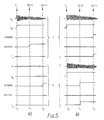
- Figure 5 shows the waveforms produced by the discriminating circuits D S and D R provided at both ends of a protected line 2, and, in particular shows how the discriminating circuits distinguish between internal and external faults.
- Figure 5 illustrates the case where the switches S are normally closed so that the stack tuning circuits normally provide a low impedance to signals within the predetermined frequency band.
- Figure 5a illustrates the situation at the discriminating circuits at both ends S and R of the line 2 when an external fault F1 as shown in Figure 1 occurs.
- the fault F1 occurs and high frequency signals are generated which are detected at the end S, as illustrated by the voltage V F passed by the filter F at end S, and by the high level signal V D at end S.
- V F passed by the filter F at end S
- V D high level signal
- the stack tuning arrangement at end S shorts the high frequency signals received to ground so that there is little high frequency received by the stack tuning arrangement at end R, as illustrated by the trace of the voltage V F at end R.
- the directional detector DD at R for example at time t2, detects the fault and generates a forward signal.
- this forward signal is provided in conjuction with a low level V D output, no trip signal T R is produced.
- the forward signal at end R opens the switch S in the associated stack tuning circuit.
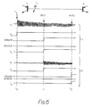
- Figure 5b shows the operation when an internal fault F2 occurs at time t o such that high frequence signals V F are output from the filters F of both discriminating circuits D S and D R .
- the output V D of the level detector changes from 0 to 1.
- the directional detectors DD at both of the ends S and R will produce forward signals which are used to open the switches S at each end and are also applied to the logic means 10 in the respective discriminating circuits D S and D R .
- the fault F2 is nearer to the end R and thus the forward signal at that end is provided at time t1, at which time a trip signal T R is generated to trip the circuit breaker 4 at that end of the line 2.
- the directional detector DD at end S produces a forward signal.
- the output V D at the end S still remains at one the trip signal T S is also generated.
- the line 2 has been isolated from the transmission system.
- each discriminating circuit of a signal having a frequency within the range of interest together with a forward signal from the directional detector is sufficient to generate a trip signal for the associated circuit breaker.
- the use of the forward signal from the directional detector to additionally open the switch S in the stack tuning circuit is unnecessary.
- the signals transmitted to the remote end would be very small if the local tuning circuit remained an effective short circuit to that signal.
- By opening the switch S in the local tuning circuit it is ensured that a sufficient signal is transmitted to the remote end. This case is illustrated in Figure 6 which shows the situation where a fault occurs close to the end S.
- Figure 7 illustrates the mode of operation where the switches in the stack tuning circuit at the ends of the protected line 2 are normally open and are closed to provide an effective short circuit by the production of a reverse signal by the appropriate directional detector DD.
- Figure 7a shows the situation where an external fault F1 occurs at time t o , causing high frequency signals to be detected by the discriminating circuit D S as shown by the waveform V F and the production of a one signal at the output V D of the level detector at end S.
- This high frequency signal is similarly detected at the end R.
- the directional detector DD at end S produces a reverse signal, which clearly does not cause the discriminating circuit D S to produce any trip signal. However, this reverse signal does close the switch S in the stack tuning circuit at end S such that the high frequency signals are effectively short circuited and are therefore no longer transmitted to the end R, where the output V D changes from one to zero.
- the directional detector DD at end R produces a forward signal, but as V D is now at zero, no trip signal is generated.
- FIG. 7b illustrates the operation upon the occurrence of a fault F2 internal to the protected line 2 where the switches S are normally open.
- the occurrence of the fault at F2 causes the high frequency signals V F to be detected at each end and thus the output signals V D to change to the one level.
- the directional detector DD nearest the fault, that is at end R produces a forward signal, and hence a trip signal T R is generated.
- the switch S in the stack tuning circuit at end R remains open circuit.
- the directional detector DD at end S produces a forward signal which, because of the level one V D signal persisting, causes the trip signal T S to be generated.
- Figures 7a and 7b again underline the need to ensure that the output voltage V D remains at level one for a time sufficient to allow for the relatively slow operation of the directional detectors.
- care needs to be taken in determining the extent to which the pulse V D is stretched.
- an eroneous signal T R would be generated. This of course, compromises the security of the scheme.
- the mode of operation in which the stack tuning circuits are operated with their switches S normally closed that is in the short circuit condition, provides the highest levels of security and dependability in practical operations.
- the centre frequency to which the stack tuning circuit and the narrow band filter are tuned can be chosen as required.
- Figure 8 schematically illustrates the situation which could arise where a large number of lines are terminated at a particular bus bar B which produces a bus bar to ground capacitance of the order of 0.2 ⁇ F.
- the bus bar capacitive reactance must be considered.
- the capacitive reactance should be at least of the order of 3 times the impedance of the stack tuning circuits when operating in the short circuit mode.
- FIG. 9a An example of a line trap circuit, which is conventional, is shown in Figure 9a.
- the circuit shown in Figure 9a effectively presents an impedance over a predetermined frequency band, which approximates closely to the line characteristic or surge impedance.
- the frequency response of the line trap circuit at Figure 9a is shown in Figure 9b plotted against frequency normalised with respect to the centre frequency.
- the bus bar capacitive reactance is relatively low so that for most practical purposes the line should be ideally terminated by line traps. At the frequencies of interest, the line trap would commonly present a resistance of the order of 300 ⁇ and this is sufficient to overcome any discrimination problems which may be caused when there is a restriction on the choice of centre frequencies.
- modulation could be simply achieved by causing the periodic opening and closing of the switches S in the stack tuning circuits.
- Figures 10 to 15 illustrate a further embodiment of the invention which is particularly useful for detecting and discriminating faults in lower voltage distribution systems, for example, having power lines carrying voltages of the order of 11kV.
- FIG 10 shows schematically a distribution feeder which is divided into a number of individual protected lines 102.
- a circuit breaker 104 is provided at each end of each line 102 so that the line can be isolated from the distribution feeder.
- a number of detecting and locating circuits DL are spaced along the distribution feeder such that a respective locating circuit DL is provided at each end of each protected line 102.
- each locating circuit DL receives signals from the two lines 102 with which it is connected.
- the detecting and locating circuits DL are tuned to a relatively narrow band of frequencies, even though, as described above, a fault in the system generally produces wideband noise.
- the centre frequency is preferably in the range 50Hz to 500kHz, a value of 300kHz again being typical, and the band may be about ⁇ 5kHz about that centre frequency.
- Each locating circuit DL has two outputs, each connected to a respective discriminator circuit DDD.
- the locating circuits DL are responsive to the narrow band frequencies of interest and their output signals indicate whether a fault is present. However, a trip signal T F is only generated when the indication of the presence of a fault is accompanied by an appropriate locative signal.
- each discriminator circuit DDD is arranged to generate locative signals to indicate the location of a fault from the two outputs received from the respective locating circuit DL.
- a switch was provided at each end of each line 2 to prevent high frequency signals at one end of the line reaching the other end of the line.
- Such switches are not provided in the embodiment of Figure 10. The switches are not needed because, as we shall see, the frequencies of interest on the line are attenuated by the detecting and locating circuits DL.
- Figure 11 shows one practical implementation of a detecting and locating circuit DL connected at one input terminal X to a downstream protected line 102, and at a second input terminal Y to an upstream protected line 102.
- the line trap circuit 140 is nominally tuned to the centre frequency fc chosen, for example, to 300kHz, and typically has an impedance of about 10Ro at that frequency, where Ro is the line surge impedance. Its frequency response, normalised with respect to the centre frequency will have a similar shape to that of Figure 9b, except that its impedance at the centre frequency will approximate to ten times the surge impedance, rather than approximately equal to it as previously.
- Each side of the line trap circuit 140 is connected to a non-switched stack tuner circuit comprising a series arrangement of a capacitor Csx, Csy, and an inductor Lsx, Lsy.
- the output voltage Vox, Voy is taken across a respective series resistor Rox, Roy and fed to the output by way of a respective isolation transformer T1, T2.
- Each tuned circuit is arranged to have its minimum impedance at the centre frequency fc, and this minimum impedance is substantially equal to the line surge impedance Ro.
- the voltage transfer characteristic of each stack tuner circuit normalised with respect to the centre frequency is illustrated in Figure 12.
- a fault F2 occurs which is external to the two protected lines 102 directly connected to the locating circuit DL2.
- high frequency signals are impressed on the line at that point. These signals arrive at the locating circuit DL3 and output signals Vox3 and Voy3 are applied to the discriminator circuit DDD3.
- the discriminator circuit DDD3 will output a trip signal T F .
- the high frequency signals arriving at the locating circuit DL3 are fed towards the locating circuit DL2 but are attenuated by the line trap circuit 140.
- the level of the in-band signals at terminal X3 with the particular circuit parameters suggested will be approximately (1/21)th of the original signal level at terminal Y3.
- the level of the in-band signals arriving at the locating circuit DL2 is therefore relatively low and the respective discriminator circuit DDD2 is arranged not to output trip signals in response to such low level signals .
- the detecting and locating circuits DL are responsive to the existence of in-band signals to detect the occurrence of a fault. Furthermore, and as previously, the discriminating circuits DDD also consider the level of the in-band signal as a further degree of discrimination in establishing the existence of a fault. However, rather than using separate direction detectors to produce location information, as previously, the arrangement of Figures 10 and 11 also utilises the level of the in-band signal to provide locative signals. As will be seen below, each locating circuit DL compares the level of the signals on each of its input terminals to establish the direction of the fault.
- Figure 13 shows an embodiment of a discriminator circuit DDD arranged to receive the output voltages Vox and Voy from an associated detecting and locating circuit DL.
- the three lines each carrying one phase of a three-phase supply, are each provided with a respective detecting and locating circuit DL and the outputs Vox and Voy of each phase are fed to a single discriminator circuit as shown in Figure 13.
- the three output voltages Voxa, Voxb, Voxc, of the three phases at one side of the locating circuit DL are first of all fed to a summation circuit 106x where they are combined using aerial mode components of propagation.
- the three outputs may be combined using a 1,0,-1, or generally a k,0,-k combination.
- the three outputs can be combined using a 1,-2,1, or more generally a n,-2n,n combination as is illustrated in Figure 13.
- the n,-2n,n combination is particularly convenient because it causes any common mode signals induced in the power lines from a remote source to be cancelled. Equally importantly, this particular combination also reduces any signals within the predetermined frequency range which are detected in a healthy circuit as a consequence of a fault in an adjacent circuit in double circuit or parallel feeder arrangements.
- the summation circuit 106x in the circuit of Figure 13 produces an output Vsx which is fed to a narrow band filter F x .
- this filter F x is a band pass filter tuned to the same centre frequency as the stack tuning arrangements.
- the filter F x will pass only those frequency signals which are in-band.
- the narrow band filter F x has a bandwidth of the order of 10kHz and therefore acts to provide additional tuning.
- the threshold voltage V T is set so that any noise in the output signal V Fx from the filter F x , for example, generated by the filter F x , the stack tuning arrangement, or the summation circuit, is effectively ignored.
- the level of the threshold voltage V T can also be set to control the sensitivity of the equipment to system faults.
- the level of the threshold voltage V T is typically a minimum of 1,000th of the maximum signal level which appears at the output of the filter F x .
- V T has the value of 20mV where the narrow band filter F x has a bandwidth of 10 kHz centred on the frequency 300 kHz.
- the three output voltages Voya, Voyb, Voyc of the three phases at the other side of the locating circuit DL are treated in substantially exactly the same manner as described above with reference to voltages Voxa, Voxb, Voxc.
- the voltages Voya, Voyb, Voyc are summed by a summation circuit 106y, the summed output is filtered by a narrow band filter F y and then the filtered output signal V Fy is applied to a level detector circuit 108y such that comparison with a threshold voltage V T determines the output signal V zy .
- the outputs V zx and V zy of the level detectors 108 are applied to logic means 110. Locative information signals, generated by the discriminator circuit DDD are also applied to the logic means 110.
- the two output signals V Fx and V Fy from the narrow band filters F x and F y are fed to a directional decision logic circuit 112. It will be appreciated that the level of these signals will have been determined in dependence upon the location of the fault. For example, for the locating circuit DL2, if the internal fault F1 occurs upstream the whole high frequency response will appear at the input terminal Y2, whilst the line trap circuit 140 will attenuate the input signal at the terminal X2. This means that the output signal Voy will be very much greater than the output signal Vox, probably by an order of 1:21. Similarly the signal V Fx output from the narrow band filter F x will be very much smaller than the signal V Fy .
- the directional decision logic circuit 112 compares the two signals V Fx and V Fy . If V Fy is greater than V Fx , as in this case, a one is produced on the output V DU to indicate the location of the fault is upstream. Similarly, if V Fx is greater than V Fy a one appears on the output V DD to indicate a downstream fault.
- the fault location signals V DU and V DD are applied to the logic means 110 which is arranged to produce a trip signal T F only if a one on V DU (upstream fault) coincides with a one on V zy or a one on V DD (downstream fault) coincides with a one on V zx .
- Figure 14 shows the waveforms of the discriminator circuits DDD1, DDD2 and DDD3 for the fault F1 occurring between terminals X3 and Y2 ( Figure 10). These waveforms indicate how internal and external faults are discriminated.
- Figure 14b shows the waveforms at discriminator circuit DDD2 which is associated with locating circuit DL2 to which the fault F1 is internal and upstream.
- the fault F1 occurs high frequency signals are generated and are passed substantially without attenuation by the upstream side of discriminator circuit DDD2 such that a high level, in-band signal V sy is applied to the narrow band filter F y .
- the high frequency signals are attenuated by the line trap circuit of discriminator circuit DDD2 such that the level of the signal V sx applied to its filter F x is less than the level of V sy . Accordingly, the output of the direction decision logic circuit 112 is a low on V DD but a high on V DU as illustrated.
- the high level signal V sy is applied by the filter F y to the level detector 108y whose output V zy will thus be high, whilst the output V zx of level detector 108x is low, again as shown in Figure 14b.
- the high signals V DU and V zy applied to the logic means 110 cause a trip signal T F to be produced.
- the internal, downstream fault F1 causes a high level signal V sx and an attenuated signal V sy to be received by the discriminator circuit DDD3. It will be appreciated that these signals cause V DD and V zx to go high, so that again a trip signal T F is generated.
- the discriminator circuit DDD1 receives attenuated high frequency signals V sx and V sy as shown in Figure 14a such that neither V zx nor V zy goes high and such that no trip signal T F is produced.
- V sy is greater than V sx such that V DU goes high to indicate an upstream fault.
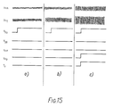
- Figures 15a, 15b, 15c show the waveforms at discriminator circuits DDD1, DDD2 and DDD3 respectively for the fault F2 occurring upstream of terminal Y3.
- Figure 15 shows graphically that whilst every discriminator circuit is able to recognise that the fault is upstream, only the discriminator circuit DDD3, to which the fault F2 is internal, outputs a trip signal because there is not a sufficient level in any of the high frequency signals applied to the discriminator circuits DDD1 and DDD2 to produce a high output from their level detectors 108x or 108y.
- Figure 15 also illustrates the progressive attenuation of the high frequency signal as it travels through the protected lines 102 and the detecting and locating circuits DL3 to DL1.
- Figure 10 shows a configuration of a distribution feeder in which a circuit breaker 104 is provided at each end of each protected line 102.
- breakers are not necessarily present at regular intervals.
- the invention may be used to indicate the location of faults rather than to isolate faulty lines.
- the distribution system may have other configurations to that shown in Figure 11.
- line taps, spurs and the like may be provided.
- appropriate detecting and locating circuits DL may still be associated with the individual lines of the distribution system.
- the stack tuning circuits utilise the stack tuning capacitor which already exists in the capacitor voltage transformer commonly provided at the end of a transmission line.
- This is advantageous because of the problems of providing a capacitor with a sufficiently high capacitance for use at the transmission line voltages. Such problems do not arise at most distribution system voltages.
- the invention has been described above with reference to the discrimination of faults in EHV transmission systems, and in distribution systems, and clearly the invention has general applicability to all transmission and distribution systems.
- the invention is generally applicable to any electrical system where faults generate signals having frequencies within a predetermined band, and in the claims and in the preamble to the specification the terms "transmission circuit” and “transmission system” are used to refer generally to electrical circuits and systems in which high frequency faults are generated.
Landscapes
- Locating Faults (AREA)
- Monitoring And Testing Of Transmission In General (AREA)
Applications Claiming Priority (2)
| Application Number | Priority Date | Filing Date | Title |
|---|---|---|---|
| GB8727490 | 1987-11-24 | ||
| GB878727490A GB8727490D0 (en) | 1987-11-24 | 1987-11-24 | Detecting faults in transmission circuits |
Publications (3)
| Publication Number | Publication Date |
|---|---|
| EP0318274A2 true EP0318274A2 (de) | 1989-05-31 |
| EP0318274A3 EP0318274A3 (en) | 1990-11-28 |
| EP0318274B1 EP0318274B1 (de) | 1996-01-17 |
Family
ID=10627454
Family Applications (1)
| Application Number | Title | Priority Date | Filing Date |
|---|---|---|---|
| EP88311098A Expired - Lifetime EP0318274B1 (de) | 1987-11-24 | 1988-11-23 | Verfahren und Vorrichtung zur Fehlerdetektierung und -diskriminierung in Energieübertragungsnetzen |
Country Status (5)
| Country | Link |
|---|---|
| US (1) | US4922368A (de) |
| EP (1) | EP0318274B1 (de) |
| JP (1) | JPH01205632A (de) |
| DE (1) | DE3854913T2 (de) |
| GB (2) | GB8727490D0 (de) |
Cited By (4)
| Publication number | Priority date | Publication date | Assignee | Title |
|---|---|---|---|---|
| WO1994006026A1 (en) * | 1992-08-27 | 1994-03-17 | The University Of Bath | Detecting faults in power lines |
| EP0657742A3 (de) * | 1993-11-24 | 1995-08-16 | At & T Corp | Einrichtung zur Erkennung von Störlichtbögen in Energiekabeln. |
| WO1996030988A1 (en) * | 1995-03-30 | 1996-10-03 | Siemens Energy & Automation, Inc. | Electric arc detector sensor circuit |
| WO2010070430A1 (en) * | 2008-12-17 | 2010-06-24 | Eaton Corporation | Power distribution system and electrical switching apparatus employing a filter trap circuit to provide arc fault trip coordination |
Families Citing this family (50)
| Publication number | Priority date | Publication date | Assignee | Title |
|---|---|---|---|---|
| JP3039936B2 (ja) * | 1989-08-25 | 2000-05-08 | 株式会社日立製作所 | 電力線の劣化判定方法及びその装置 |
| US5185686A (en) * | 1991-03-28 | 1993-02-09 | Eaton Corporation | Direction sensing arc detection |
| US5185687A (en) * | 1991-03-28 | 1993-02-09 | Eaton Corporation | Chaos sensing arc detection |
| US5185684A (en) * | 1991-03-28 | 1993-02-09 | Eaton Corporation | Frequency selective arc detection |
| US5185685A (en) * | 1991-03-28 | 1993-02-09 | Eaton Corporation | Field sensing arc detection |
| US5208542A (en) * | 1991-03-28 | 1993-05-04 | Eaton Corporation | Timing window arc detection |
| US5434509A (en) * | 1992-07-30 | 1995-07-18 | Blades; Frederick K. | Method and apparatus for detecting arcing in alternating-current power systems by monitoring high-frequency noise |
| US5432455A (en) * | 1992-07-30 | 1995-07-11 | Blades; Frederick K. | Method and apparatus for detecting arcing in alternating current power systems by monitoring high-frequency noise |
| US5729145A (en) * | 1992-07-30 | 1998-03-17 | Siemens Energy & Automation, Inc. | Method and apparatus for detecting arcing in AC power systems by monitoring high frequency noise |
| US5452223A (en) * | 1993-08-20 | 1995-09-19 | Eaton Corporation | Arc detection using current variation |
| SE502073C2 (sv) * | 1994-01-03 | 1995-07-31 | Asea Brown Boveri | Förfarande och anordning för riktningsbestämning av fel på en kraftlinje |
| US6246556B1 (en) | 1995-03-13 | 2001-06-12 | Square D Company | Electrical fault detection system |
| US5825598A (en) * | 1997-02-11 | 1998-10-20 | Square D Company | Arcing fault detection system installed in a panelboard |
| US6242993B1 (en) | 1995-03-13 | 2001-06-05 | Square D Company | Apparatus for use in arcing fault detection systems |
| US6313641B1 (en) | 1995-03-13 | 2001-11-06 | Square D Company | Method and system for detecting arcing faults and testing such system |
| US6377427B1 (en) | 1995-03-13 | 2002-04-23 | Square D Company | Arc fault protected electrical receptacle |
| US5682101A (en) | 1995-03-13 | 1997-10-28 | Square D Company | Arcing fault detection system |
| US6452767B1 (en) | 1995-03-13 | 2002-09-17 | Square D Company | Arcing fault detection system for a secondary line of a current transformer |
| US6532424B1 (en) | 1995-03-13 | 2003-03-11 | Square D Company | Electrical fault detection circuit with dual-mode power supply |
| US6034611A (en) * | 1997-02-04 | 2000-03-07 | Square D Company | Electrical isolation device |
| US6259996B1 (en) | 1998-02-19 | 2001-07-10 | Square D Company | Arc fault detection system |
| US6313642B1 (en) | 1995-03-13 | 2001-11-06 | Square D Company | Apparatus and method for testing an arcing fault detection system |
| US5834940A (en) * | 1996-09-24 | 1998-11-10 | Brooks; Stanley J. | Arcing fault detector testing and demonstration system |
| US5839092A (en) * | 1997-03-26 | 1998-11-17 | Square D Company | Arcing fault detection system using fluctuations in current peaks and waveforms |
| US5946179A (en) * | 1997-03-25 | 1999-08-31 | Square D Company | Electronically controlled circuit breaker with integrated latch tripping |
| US5847913A (en) * | 1997-02-21 | 1998-12-08 | Square D Company | Trip indicators for circuit protection devices |
| US6477021B1 (en) | 1998-02-19 | 2002-11-05 | Square D Company | Blocking/inhibiting operation in an arc fault detection system |
| US5986860A (en) * | 1998-02-19 | 1999-11-16 | Square D Company | Zone arc fault detection |
| US6621669B1 (en) | 1998-02-19 | 2003-09-16 | Square D Company | Arc fault receptacle with a feed-through connection |
| US6625550B1 (en) | 1998-02-19 | 2003-09-23 | Square D Company | Arc fault detection for aircraft |
| US6782329B2 (en) | 1998-02-19 | 2004-08-24 | Square D Company | Detection of arcing faults using bifurcated wiring system |
| US6567250B1 (en) | 1998-02-19 | 2003-05-20 | Square D Company | Arc fault protected device |
| US6275044B1 (en) | 1998-07-15 | 2001-08-14 | Square D Company | Arcing fault detection system |
| US6453248B1 (en) * | 1998-07-21 | 2002-09-17 | Abb Inc. | High impedance fault detection |
| GB9820141D0 (en) | 1998-09-17 | 1998-11-11 | Alstom Uk Ltd | Improved fault protection scheme |
| GB2345810B (en) * | 1999-01-13 | 2003-07-23 | Alstom Uk Ltd | Fault-detection apparatus |
| US6987389B1 (en) * | 2000-11-14 | 2006-01-17 | Pass & Seymour, Inc. | Upstream/downstream arc fault discriminator |
| GB2375242A (en) * | 2001-05-03 | 2002-11-06 | Alstom | Protecting a section of an electrical power line |
| US7068480B2 (en) | 2001-10-17 | 2006-06-27 | Square D Company | Arc detection using load recognition, harmonic content and broadband noise |
| US7151656B2 (en) | 2001-10-17 | 2006-12-19 | Square D Company | Arc fault circuit interrupter system |
| US7136265B2 (en) * | 2001-10-17 | 2006-11-14 | Square D Company | Load recognition and series arc detection using bandpass filter signatures |
| GB2388482B (en) * | 2002-05-07 | 2005-06-15 | Alstom | Improved power line protection |
| BRPI0512994B1 (pt) * | 2004-07-05 | 2017-12-05 | Pepperl & Fuchs | "electric circuit with flammable arc prevention device" |
| US7253637B2 (en) | 2005-09-13 | 2007-08-07 | Square D Company | Arc fault circuit interrupter system |
| US20110181295A1 (en) * | 2010-01-22 | 2011-07-28 | Livewire Test Labs, Inc. | Fault detection using combined reflectometry and electronic parameter measurement |
| US8659862B2 (en) * | 2010-09-10 | 2014-02-25 | Ssi Power, Llc | Directional fault location and isolation system |
| US9551751B2 (en) | 2011-06-15 | 2017-01-24 | Ul Llc | High speed controllable load |
| EP3053235A4 (de) | 2013-09-30 | 2017-06-28 | Schneider Electric USA, Inc. | Verteilter lichtbogenfehlerschutz zwischen ausgang und schutzschalter |
| US9502882B2 (en) * | 2014-04-04 | 2016-11-22 | Eaton Corporation | Fault detection and zone location system |
| EP3093675B1 (de) * | 2015-05-14 | 2019-01-16 | General Electric Technology GmbH | Verbesserungen an oder im zusammenhang mit gleichstromschutzschemata |
Family Cites Families (9)
| Publication number | Priority date | Publication date | Assignee | Title |
|---|---|---|---|---|
| DE277967C (de) * | ||||
| CH105100A (de) * | 1923-04-26 | 1924-06-02 | Oerlikon Maschf | Verfahren und Einrichtung zum Schutz elektrischer Anlagen gegen unerwünschte Funken- und Lichtbogenbildung. |
| DE543951C (de) * | 1925-05-28 | 1932-02-12 | Carl Schmittutz | Einrichtung zum selektiven Abschalten fehlerhafter Leitungsstrecken |
| SE368092B (de) * | 1972-11-06 | 1974-06-17 | Asea Ab | |
| DE2559100A1 (de) * | 1975-12-30 | 1977-07-07 | Joachim Pauls | Verfahren zum schutz elektrischer freileitungen und deren armaturen vor spannungsueberschlaegen und lichtboegen und deren folgen |
| US4466071A (en) * | 1981-09-28 | 1984-08-14 | Texas A&M University System | High impedance fault detection apparatus and method |
| US4438475A (en) * | 1982-08-02 | 1984-03-20 | Westinghouse Electric Corp. | Ultra-high speed protective relay apparatus and method for providing single pole switching |
| US4538196A (en) * | 1983-04-22 | 1985-08-27 | Westinghouse Electric Corp. | Protective relay apparatus and method for providing single-pole tripping |
| US4751604A (en) * | 1986-10-16 | 1988-06-14 | General Electric Company | Comparison signal error detector for protective relay system |
-
1987
- 1987-11-24 GB GB878727490A patent/GB8727490D0/en active Pending
-
1988
- 1988-11-23 GB GB8827366A patent/GB2212998B/en not_active Expired - Lifetime
- 1988-11-23 US US07/275,723 patent/US4922368A/en not_active Expired - Fee Related
- 1988-11-23 EP EP88311098A patent/EP0318274B1/de not_active Expired - Lifetime
- 1988-11-23 DE DE3854913T patent/DE3854913T2/de not_active Expired - Fee Related
- 1988-11-24 JP JP63297135A patent/JPH01205632A/ja active Pending
Cited By (7)
| Publication number | Priority date | Publication date | Assignee | Title |
|---|---|---|---|---|
| WO1994006026A1 (en) * | 1992-08-27 | 1994-03-17 | The University Of Bath | Detecting faults in power lines |
| US5796257A (en) * | 1992-08-27 | 1998-08-18 | The University Of Bath | Detecting faults in power lines |
| EP0657742A3 (de) * | 1993-11-24 | 1995-08-16 | At & T Corp | Einrichtung zur Erkennung von Störlichtbögen in Energiekabeln. |
| WO1996030988A1 (en) * | 1995-03-30 | 1996-10-03 | Siemens Energy & Automation, Inc. | Electric arc detector sensor circuit |
| US5706159A (en) * | 1995-03-30 | 1998-01-06 | Siemens Energy & Automation, Inc. | Circuit interrupter including an electric arc monitoring circuit |
| WO2010070430A1 (en) * | 2008-12-17 | 2010-06-24 | Eaton Corporation | Power distribution system and electrical switching apparatus employing a filter trap circuit to provide arc fault trip coordination |
| US8040644B2 (en) | 2008-12-17 | 2011-10-18 | Gaton Corporation | Power distribution system and electrical switching apparatus employing a filter trap circuit to provide arc fault trip coordination |
Also Published As
| Publication number | Publication date |
|---|---|
| US4922368A (en) | 1990-05-01 |
| GB2212998B (en) | 1992-02-05 |
| GB8827366D0 (en) | 1988-12-29 |
| JPH01205632A (ja) | 1989-08-18 |
| GB2212998A (en) | 1989-08-02 |
| EP0318274B1 (de) | 1996-01-17 |
| GB8727490D0 (en) | 1987-12-23 |
| DE3854913D1 (de) | 1996-02-29 |
| DE3854913T2 (de) | 1996-05-30 |
| EP0318274A3 (en) | 1990-11-28 |
Similar Documents
| Publication | Publication Date | Title |
|---|---|---|
| EP0318274B1 (de) | Verfahren und Vorrichtung zur Fehlerdetektierung und -diskriminierung in Energieübertragungsnetzen | |
| EP0507782B1 (de) | Spektrumerfassung von lichtbögen und radiofrequenzen | |
| US4153923A (en) | Ground monitoring system and method | |
| US5477150A (en) | Electric arc and radio frequency spectrum detection | |
| US4896241A (en) | Directional comparison blocking protective relay system | |
| US10345363B2 (en) | High-fidelity voltage measurement using resistive divider in a capacitance-coupled voltage transformer | |
| US10802054B2 (en) | High-fidelity voltage measurement using a capacitance-coupled voltage transformer | |
| US4234901A (en) | Protective relay apparatus | |
| Sanders et al. | Power line carrier channel & application considerations for transmission line relaying | |
| EP0963025B1 (de) | Detektion eines fehlerhaftes elektrisches Leistungskabels bei Erdschluss in einem elektrischen Verteilernetz | |
| US4538195A (en) | Three terminal current differential protective relay | |
| US4317151A (en) | Apparatus for fault direction-comparison protection | |
| US3312866A (en) | Distance relay actuated phase comparison relaying device | |
| Fitzgerald | A carrier-current pilot system | |
| US4115668A (en) | Echo suppressor with SF transmission and regeneration | |
| EP0657033B1 (de) | Nachweis von störungen in starkstromleitungen | |
| US3710188A (en) | High tension network distribution system | |
| Patterson et al. | Directional comparison blocking system fundamentals | |
| USRE19034E (en) | fitz gerald | |
| US1797976A (en) | Fault-responsive apparatus | |
| Kitagawa et al. | Newly Developed FM Current-Differential Carrier Relaying System and its Field Experiences | |
| Johns et al. | A novel non-unit protection scheme based on fault generated high frequency noise on transmission lines | |
| US4878241A (en) | Audio frequency interface for differential relays | |
| GB2235342A (en) | Apparatus for detecting a fault in a transmission line | |
| Wedepohl | Information Links |
Legal Events
| Date | Code | Title | Description |
|---|---|---|---|
| PUAI | Public reference made under article 153(3) epc to a published international application that has entered the european phase |
Free format text: ORIGINAL CODE: 0009012 |
|
| AK | Designated contracting states |
Kind code of ref document: A2 Designated state(s): CH DE FR LI |
|
| 17P | Request for examination filed |
Effective date: 19890926 |
|
| PUAL | Search report despatched |
Free format text: ORIGINAL CODE: 0009013 |
|
| AK | Designated contracting states |
Kind code of ref document: A3 Designated state(s): CH DE FR LI |
|
| RAP1 | Party data changed (applicant data changed or rights of an application transferred) |
Owner name: BRITISH TECHNOLOGY GROUP PLC |
|
| RAP3 | Party data changed (applicant data changed or rights of an application transferred) |
Owner name: BRITISH TECHNOLOGY GROUP LTD |
|
| 17Q | First examination report despatched |
Effective date: 19921211 |
|
| GRAA | (expected) grant |
Free format text: ORIGINAL CODE: 0009210 |
|
| AK | Designated contracting states |
Kind code of ref document: B1 Designated state(s): CH DE FR LI |
|
| PG25 | Lapsed in a contracting state [announced via postgrant information from national office to epo] |
Ref country code: FR Effective date: 19960117 |
|
| REF | Corresponds to: |
Ref document number: 3854913 Country of ref document: DE Date of ref document: 19960229 |
|
| EN | Fr: translation not filed | ||
| PLBE | No opposition filed within time limit |
Free format text: ORIGINAL CODE: 0009261 |
|
| STAA | Information on the status of an ep patent application or granted ep patent |
Free format text: STATUS: NO OPPOSITION FILED WITHIN TIME LIMIT |
|
| 26N | No opposition filed | ||
| PGFP | Annual fee paid to national office [announced via postgrant information from national office to epo] |
Ref country code: DE Payment date: 19981023 Year of fee payment: 11 |
|
| PGFP | Annual fee paid to national office [announced via postgrant information from national office to epo] |
Ref country code: CH Payment date: 19990218 Year of fee payment: 11 |
|
| PG25 | Lapsed in a contracting state [announced via postgrant information from national office to epo] |
Ref country code: LI Free format text: LAPSE BECAUSE OF NON-PAYMENT OF DUE FEES Effective date: 19991130 Ref country code: CH Free format text: LAPSE BECAUSE OF NON-PAYMENT OF DUE FEES Effective date: 19991130 |
|
| PG25 | Lapsed in a contracting state [announced via postgrant information from national office to epo] |
Ref country code: DE Free format text: LAPSE BECAUSE OF NON-PAYMENT OF DUE FEES Effective date: 20000901 |
|
| REG | Reference to a national code |
Ref country code: CH Ref legal event code: NV Representative=s name: KIRKER & CIE SA |