EP0318311A2 - Übergang zwischen zwei Streifenleitungen - Google Patents
Übergang zwischen zwei Streifenleitungen Download PDFInfo
- Publication number
- EP0318311A2 EP0318311A2 EP88311185A EP88311185A EP0318311A2 EP 0318311 A2 EP0318311 A2 EP 0318311A2 EP 88311185 A EP88311185 A EP 88311185A EP 88311185 A EP88311185 A EP 88311185A EP 0318311 A2 EP0318311 A2 EP 0318311A2
- Authority
- EP
- European Patent Office
- Prior art keywords
- conductor
- dielectric layer
- stripline
- coaxial
- pads
- Prior art date
- Legal status (The legal status is an assumption and is not a legal conclusion. Google has not performed a legal analysis and makes no representation as to the accuracy of the status listed.)
- Granted
Links
Images



Classifications
-
- H—ELECTRICITY
- H01—ELECTRIC ELEMENTS
- H01P—WAVEGUIDES; RESONATORS, LINES, OR OTHER DEVICES OF THE WAVEGUIDE TYPE
- H01P3/00—Waveguides; Transmission lines of the waveguide type
- H01P3/02—Waveguides; Transmission lines of the waveguide type with two longitudinal conductors
- H01P3/08—Microstrips; Strip lines
- H01P3/085—Triplate lines
-
- H—ELECTRICITY
- H01—ELECTRIC ELEMENTS
- H01P—WAVEGUIDES; RESONATORS, LINES, OR OTHER DEVICES OF THE WAVEGUIDE TYPE
- H01P1/00—Auxiliary devices
- H01P1/04—Fixed joints
- H01P1/047—Strip line joints
Definitions
- the invention relates to a transition between stripline transmission lines that is efficient at microwave frequencies and readily fabricated.
- stripline transmission lines are in common use.
- the advantage of such circuits is that they may be patterned by an automated photographic process that allows for efficient electrical design.
- Stripline provides not only efficient high frequency runs from point to point, but many important passive functions such as impedance transformation, delay, filtering, power division or combination, and directional coupling.
- stripline A major limitation of stripline occurs when it is desired to effect cross-overs.
- circuits applications in which cross-overs are required.
- the cross-over issue is presented in monitoring a four element antenna circuit of a phased array radar system for amplitude and phase.
- Cost constraints dictate that four antenna drive circuits be placed in a common package with four dipole antennas, four independent signal paths including filters to the four dipole antennas and four monitoring or calibrating paths.
- the monitoring which may originate from one point, must in principle, cross at least two of the four antenna signal paths, if each signal path is to be monitored.
- Cross-over in the antenna stripline circuit is achieved by use of two coaxial transitions from a singly branched monitoring circuit also in stripline, and placed on the main antenna circuit.
- the two branches of the monitoring circuit enter the stripline of the antenna circuit at two transitions disposed between pairs of antenna paths.
- the monitoring circuit is then branched a second time on the antenna circuit, and the four branches are then coupled to the four antenna signal paths without further ado.
- transitions at microwave frequencies represent a problem as well as a solution to the cross-over problem.
- the transition taking into account the constraints of stripline manufacture, and the small thickness dimensions in which a transition may occur, ordinarily create objectionable mismatches, electrical discontinuities, and parasitic reactances at such transitions.
- the customary result of these factors is to make transitions less than optimum at microwave frequencies.
- a transition embodying the invention can be simple in design, be readily manufactured by means compatible with printed circuit materials and processes, and provide high performance at microwave frequencies.
- the present invention provides a combination comprising a mechanically rigid chassis, a first and a second electronic circuit employing stripline transmission lines attached to the chassis, the ground planes of the two striplines being arranged adjacent one another and in electrical contact, and a novel coaxial transition between the striplines.
- the coaxial transition comprises a first and a second continuation of the conductors of the two striplines terminating in a pair of pads.
- the pads are disposed in mutually facing positions centered upon a common axis perpendicular to the layers of the striplines, with the paths to the pads approaching the axis from a common azimuth.
- the coaxial transition further comprises a cylindrical conductor forming the inner conductor of the coaxial section aligned along the axis and interconnecting the pads, and a sequence of thin conductors parallel to the axis, arranged in a cylindrical surface centered upon the axis to form the outer shield.
- the sequence is interrupted at the appropriate azimuth to admit connections.
- the thin conductors extend through the four ground planes, and are connected to each ground plane to ground the coaxial shield.
- each conductor in the shield has a flange at the center for contact with one of the internal ground planes, the conductors being disposed in holes penetrating the two circuits, with the ends soldered to the external ground planes.
- the inner cylindrical member is of a partly resilient construction compressed in the assembly to provide a good contact between pads.
- the transition performs well at microwave frequencies, although the connectors between pads and the inner coaxial conductor exhibit significant shunt capacity tending to reduce high frequency performance.
- Good high frequency performance is achieved by making the characteristic impedance of the coaxial transmission line greater than that of the stripline to introduce series inductance in the coaxial transition, and the stripline paths are narrowed near the connection to the inner coaxial conductor to reduce shunt capacity, increase the characteristic impedance and introduce additional series inductance, to further improve the high frequency performance.
- the shield is made of a thin copper sheet in a printed pattern having an elongated central region with thin conductors extending from the two elongated sides.
- the shield is bent into an uncomplete cylindrical configuration. Punched out tabs from the central region and the ends of the thin conductors make contact with the ground planes.
- a one piece construction of the coaxial shield facilitates assembly of the transition.
- Figure 1 shows a chassis, from which the cover plate has been removed, containing the electronic circuits used to operate four elements of a phased array in a radar system operating from 5 to 6 GHz.
- a high performance phased array radar system may be expected to have from 2,000 to 4,000 antenna elements at this frequency. Assuming that each chassis couples to four such antenna elements, one may expect from 500 to 1,000 such chassis in one system.
- the antenna elements are spaced from about one-half to two-thirds wavelengths apart, depending upon the scanning range. If a relatively low vertical scanning range is contemplated, the vertical spacing of the antenna elements, may be about two-thirds of a wavelength. If a relatively large horizontal scanning range is contemplated, the horizontal spacing between dipole elements will be about one-half wavelength.
- the antenna elements, if dipoles, will be oriented in a vertical plane, under these assumptions because of the greater available space in the vertical direction.
- the electronic circuits which operate four antenna elements, fall within an overall cross-sectional dimension of 16 cm x 2.7 cm, or 4 cm x 2.7 cm per antenna element, which is compact enough to lie within the available spacing at 5 to 6 GHz.
- the electronic circuits assembled within the chassis which with the chassis may be called a "sub-assembly"
- the operating electronics includes an antenna distribution circuit 11 , a phase shifter and T/R circuit 12 , and a "beam-former” distribution circuit 13 .
- the control circuits, together with local power supplies may be included in the sub-assembly to implement the steering commands to the phase shifter from a remote control computer.
- the antenna distribution circuit or antenna-monitor-filter board 11 has three functions. In transmission, it couples the outputs of four high power amplifiers on an individual basis to each of four antenna elements which radiate the radar pulse. In reception, the echoes are received by the four antenna elements, and the antenna distribution network delivers the signal returns on an individual basis to each of four low noise amplifiers. Monitoring and calibration which occurs during transmission and when reception is inhibited, permits every module in the array to be examined. During transmission, the transmit power and transmit phase are checked by a signal derived from the monitoring path. When reception is inhibited, a test signal is introduced in a monitoring path which is used to test receive gain, receive phase. The logic functionality is tested in both states.
- the filtering is designed to eliminate RF energy from external sources and to reduce the second and third harmonic content in the transmitter signal.
- the antenna distribution circuit 11 is passive, and is carried out using stripline transmission lines, which provide good shielding between circuits in the chassis, at low cost, and with the necessary compactness.
- the beamformer distribution circuit 13 distributes a signal multiplexed from four separate receiving antennas to a single channel leading to the beamformer during reception, and similarly couples signals from the beamformer intended to operate upon four antenna elements.
- the beamformer distribution circuit has no active elements, and is preferrably carried out using stripline transmission lines.
- the phase shifter and T/R circuit or "module" 12 is connected between the antenna distribution circuit and the beamformer distribution circuit which has separate parts for transmission and reception.
- a beam steering command is carried out in the phase shifter for each individual module affecting the shape and direction of the transmitting beam.
- a beam steering command is also carried out in the phase shifter for each individual module, the phase shifter being bi-directional.
- the shape and direction of the receiving beam is affected by the command.
- the T/R circuit on the module insures the proper routing of the signals through the module.
- “monitoring" which allows one to test either in the transmit direction through the phase shifter or in the receive direction through the phase shifter, one may determine errors in either state, and thus provide a correction signal appropriate to either state.
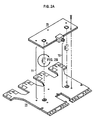
- the antenna monitor filter board 11 is best seen in the exploded view of Figure 2A which illustrates its formation from two stripline circuits 14, 15 applied face-to-face and electrically interconnected by two stripline to stripline coaxial transitions, illustrated in more detail in Figure 2B.
- the antenna monitor filter 11 consists of four parallel stripline circuits, one set of ends of which occurs at the pads P1-P4 at the bottom of the figure and the other set of ends of which occurs at the antenna A1-A4.
- Each pad e.g. P1 leads via stripline of nominally 50 ohms impedance, successively to a bandpass filter (BF1, etc), to a second and third harmonic trap (HTF1, etc), to a -20 DB directional coupler (DC1, etc) and via an unbalanced to balanced stripline antenna feed (UB1, etc) to a dipole antenna element (A1, etc).
- the directional coupler (DC1, etc) is a -20 DB coupler action in the monitoring process.
- the dirctional coupler is designed to couple a small portion of the transmitted signal fed to the antenna to a first Wilkinson power splitter PS1, used in a combining mode during transmitter operation.
- the power splitter PS1 supplies the signal sampled from the first pad P1 and the signal sampled form the second pad P2 to the power splitter output at the short length of stripline 18 leading to the first stripline to stripline transition T1.
- a second Wilkinson power splitter also used in a combining mode, supplies the signal sampled from the third pad P3 and the signal sampled from the fourth pad P4 to the power splitter output of the short length of stripline 19 leading to the second stripline to stripline transition T2.
- the monitor circuit is completed in the top board 15 , the circuit of which is illustrated in Figure 4.
- the top board includes a third Wilkinson power splitter PS3, to the output of which all four samples are supplied.
- the samples fed from the individual -20 DB couplers into the single monitoring path are fed to a single coaxial terminal, best seen in Figure 1.
- a coaxial path is provided leading to a single monitoring connector at the back edge of the quadrapack.
- the antenna monitor filter circuit 11 filters the output of each module 12, eliminating the second and third harmonic and coupling the principal energy to the dipole antenna element, less only a small amount of energy supplied by the -20 DB coupler C1 to the monitoring circuit.
- the antenna circuit carries a signal return lock to the modules (12).
- the filter (BPF1-BPF4) is in the return path, where it serves to eliminate signals outside of the filter passband.
- the second role of the monitor is to determine the receiver gain, the phase response, and the responsiveness of the module in reception to computer control. In this mode of operation, a predetermined signal is supplied to the coaxial terminal at the back of the chassis via the first Wilkinson power splitter now PS3 and then successively to the other Wilkinson power splitters PS1 and PS2.
- the signal is selectively coupled through the -20 DB coupler via the filters HT1, etc and VPF2 etc to the individual pads P1-P4 leading to the module.
- the filters HT1, etc and VPF2 etc are selectively coupled through the -20 DB coupler via the filters HT1, etc and VPF2 etc to the individual pads P1-P4 leading to the module.
- the stripline to stripline coaxial transitions used to connect the two circuit boards 14 and 15 for antenna monitoring and filtering are shown in the exploded view of Figures 2A and 2B and in the plan view of Figures 3 and 4.
- the construction of the transitions involves a minimum increase in corss-section over that required for the two striplines alone, avoids leakage of the RF fields into surrounding space and has a low loss and low VSWR characteristic of a good transition.
- both boards 14 and 15 making up the antenna monitoring and filtering boards are fastened to the chassis with five mounting screws which pass through both boards and which secure them in place against the bottom of the chassis.
- both boards are of similar construction being formed of a first and second dielectric layer with conductors forming the signal paths disposed on only one dielectric layer, between the dielectric layers.
- a first and second ground plane is provided on the outer surfaces of the dielectric layers of each circuit board.
- the lower circuit board 14 employs stripline transmission to the input transition connected to the modules 12 and to the unbalanced to balanced antenna feeds at the dipole antennas.
- the lowe board has an upper D1 and lower D2 dielectric layer between which the signal conductor C1 is supported.
- the lower ground plane G2 of the lower board 14 is complete, until it enters the front frame 16, which provides the ground plane for the antenna array at that point, the ground plane is etched into a dipole antenna configuration similar to that shown on the upper ground plane of the lower board with the dipole areas etched away.
- the upper ground plane G1 of the lower board is thus complete to the front frame 16 where a transition into the dipole elements occurs as illustrated.
- the upper circuit board 15 also has a first D1 and a second D2 dielectric layer with a conductor C2 forming the signal path, disposed between the layers.
- the outer surfaces of the dielectric layers D3 and D4 are covered with the ground planes G3 and G4 respectively.
- the underlying ground plane G4 of the upper board 15 is removed in the circular areas surrounding the transition T1 and T2.
- the removal is large enough to avoid individual spot-faced recesses, provided to accommodate the flanges 26 of the pins 25 used to form the coaxial shell in the transition.
- the area of ground plane removal is small enough as not to interfere with the continuity of the ground planes of the two striplines.
- the transition T1 consists of a continuation of a first conductor on the lower stripline 14 which has a narrow end section 19 terminating in a pad 20 and a second similar continuation of the second conductor C2 on the upper stripline 15 also comprising a narrowed section 21 terminating in a second pad 22.
- the pads are disposed in mutually facing positions centered on a common axis perpendicular to the planes of the dielectric layers.
- a concentric two-part pin 23, 24 aligned with the common axis interconnects the respective pads 20, 22.
- the transition further comprises a sequence of nine pin-shaped conductors 25 all oriented parallel to the common axis and all arranged in a cylindrical surface centered upon the common axis.
- the pin-shaped conductors 25 form a coaxial shield about the third conductor 23-24 and facilitate coaxial transmission between the respective stripline circuits.
- the signal conductors C1 and C2 enter the transition from common azimuthal positions in their respective planes. More particularly, the members C1 and C2 are oriented in a path perpendicular to the outer edge of the circuit board 14 (at the antennas) and extending inwardly toward the inner edge of the circuit board, toward the modules 12.
- the lower conductor C1 accordingly, extends toward the center of the circle in which the pins 25 have been grouped. As illustrated, nine pin holes are provided at 36° intervals, evenly spaced around the cylinder with a 72° gap, provided by the absense of a tenth pin to permit unobstructed entry of the strip conductor C1 into the center of the ring.
- the center conductor of the coaxial tranmission path is provided by the conductors 23, 24 connected between the pads 20 and 22.
- the layers D1, G2 and D4, G4 are perforated to provide a cylindrical recess of the diameter of the center conductor between the pads 20 and 22.
- the center conductor is of two-parts, consisting of a lower solid brass member 23 which is approximately of equal length to a second resilient conductor 24.
- the conductor 24 is a resiliently coiled conductive ball of gold, termed a "fuzz button".
- the outer conductor or shield of the coaxial transmission path is provided by the nine brass pins 25.
- the pins are provided with rings 26 at approximately their mid-section, and two aligned sets of nine holes are provided in the lower and upper boards to house the pins in the finished assembly.
- the rings 26 on each of the brass pins 25 are soldered to the intermediate ground plane G1.
- the pins are made slightly longer than the thicknesses of the boards and emerge through the ground planes G2 and G3 to which they are soldered to complete the electrical contact.
- the pins provide segments of a surface which is directly connected to ground planes and which is capable of providing the grounded shield of a coaxial transmission path.
- the electrical performance of the transition has been found to be excellent over a desired band of frequencies, the performance being evidenced by a low VSWR of low loss.
- the illustrated embodiment exhibits a VSWR of less than 1.09 throughout the 5 to 6 GHZ band, corresponding to a S11 loss of less than -26 DB and a S21 loss of approximately 0.5 DB.
- the measure ments are substantially the same for either direction of transmission.
- the stripline conductors C1 and C2, before they enter the transition, have a width of 0.100" (2.54mm) and are supported between two 0.0625" (1.59mm) thick Duroid layers having a dielectric constant of 2.2, each dielectric layer backed with a ground plane.
- the design produces a 50 ohm characteristic impedance.
- the coaxial line portion of the transition has a characteristic impedance set by the selection of the diameters of the center conductor, the outer pins, the diameters of the ring of outer and the dielectric constant of the dielectric material filling the structure.
- the diameter of the center conductor is 0.067" (1.70mm)
- of the outer pins is 0.042" (1.07mm)
- the coaxial line portion has a characteristic impedance of about 63 ohms.
- each conductor C1, C2 enters the ring of outer pins, its width is reduced to .070" (1.78mm) for a distance of .075" (1.90mm) and it terminates in a pad which is .080"(2.03mm) wide and .090"(2.29mm) long.
- the center of the pad coincides with the center of the cylindrical pin at the center of the coaxial line section.
- the stripline conductor is to raise the characteristic impedance to 71 ohms (approximately) at the necks (19, 21) and to drop it to 56 ohms at the pads (20, 22).
- the mismatch to the coaxial section is reduced, so that the virtual shunt capacitance is reduced, and the two features (19, 20) and (21, 22) may each be regarded as introducing a series inductance in position adjacent to the pi network.
- the end result is further improved high frequency performance at 5.5 GHZ.
- the design succeeds, and does so in a reproducable manner.
- the design is one which is easily “trimmed” to provide optimized performance over a designated band of frequencies in the microwave spectrum.
- the trimming involves the strip concuctor paths which are patterned by a photographic process. Accordingly, once trimming of a practical circuit has taken place, the critical features are readily perpetuated in a new pattern, which may be used for subsequent reproduction.
- FIG. 5 A second embodiment of a stripline to stripline transition, which is more easily assembled and of lower cost, is illustrated in Figure 5.
- the electrical design issues are essentially as before.
- the members illustrated in Figure 5 and repeated in Figure 2 bear reference numerals, raised by ten over the original reference numerals.
- a one piece shield formed by photographically patterning a sheet of thin (.003-.005"/.076-.127mm) copper.
- the sheet is patterned to consist of an elongated central section (42) with a first (43) and a second (44) sequence of thin conductors extending out from the long sides of the central section.
- the central section 42 is provided with a series of short tabs 45 achieved by punching out material from the central section. The tabs are aligned in a row parallel to the long sides of the central section, and they extend in a direction perpendicular to the plane of the sheet.
- the copper sheet is then bent into a cylindrical surface with the tabs 45 extending outwardly.
- the first 43 and second 44 sequence of thin conductors extending in mutually opposite directions from the long sides of the central section. In bending, the sheet forms an incomplete cylinder, with an interruption or opening of approximately 72° through which the connections to the stripline conductors are admitted.
- the cylindrical sheet is installed in cylindrical recess provided in the dielectric layers D14 and D11.
- the upper and lower edges of the central cyclindrical surface thus extend through the dielectric layers D14 and D11 and come into contact with the dielectric layers D13 and D12.
- the recess has an inner diameter equal to the outer diameter of the member 41 to provide external support.
- a disc 38 having an outer diameter equal to the inner diameter of the member 41 provides internal support.
- the disc 38 is further provided with a central aperture designed to accept and support the cylindrical conductor made up of the elements 33 and 34.
- Grounding of the member 41 is achieved by the thin conductors and tabs.
- One sequence (43) of thin conductors extends through holes provided in the dielectric layer D14 and the ground plane G13.
- the other sequence (44) of thin conductors extends through holes provided in the dielectric layer D12 and the ground plane G12. The portions of the thin conductors extending beyond the ground planes are then peened over and soldered.
- the tabs 45 make electrical contact with either the ground plane G11 or G14 or both and rely on a resilient compression fit.
- the dielectric material herein employed may be one of several available microwave laminates. They are characterized by a low dielectric constant (e.g. 2.2), good tensile, and compressive properties, and a low coefficient of thermal expansion in a plane parallel to the lamina.
Landscapes
- Waveguide Aerials (AREA)
- Shielding Devices Or Components To Electric Or Magnetic Fields (AREA)
- Control Of Motors That Do Not Use Commutators (AREA)
Applications Claiming Priority (2)
| Application Number | Priority Date | Filing Date | Title |
|---|---|---|---|
| US126037 | 1987-11-27 | ||
| US07/126,037 US4816791A (en) | 1987-11-27 | 1987-11-27 | Stripline to stripline coaxial transition |
Publications (3)
| Publication Number | Publication Date |
|---|---|
| EP0318311A2 true EP0318311A2 (de) | 1989-05-31 |
| EP0318311A3 EP0318311A3 (en) | 1990-05-23 |
| EP0318311B1 EP0318311B1 (de) | 1995-02-22 |
Family
ID=22422662
Family Applications (1)
| Application Number | Title | Priority Date | Filing Date |
|---|---|---|---|
| EP88311185A Expired - Lifetime EP0318311B1 (de) | 1987-11-27 | 1988-11-25 | Übergang zwischen zwei Streifenleitungen |
Country Status (3)
| Country | Link |
|---|---|
| US (1) | US4816791A (de) |
| EP (1) | EP0318311B1 (de) |
| DE (1) | DE3853135T2 (de) |
Cited By (16)
| Publication number | Priority date | Publication date | Assignee | Title |
|---|---|---|---|---|
| FR2678436A1 (fr) * | 1991-06-28 | 1992-12-31 | Trt Telecom Radio Electr | Prise coaxiale pour circuit hyperfrequence. |
| WO1994002970A1 (en) * | 1992-07-23 | 1994-02-03 | Cambridge Computer Limited | Rf waveguide signal transition apparatus |
| WO1998009341A1 (en) * | 1996-08-30 | 1998-03-05 | The Whitaker Corporation | Improved isolation in multi-layer structures |
| WO1998027793A1 (en) * | 1996-12-16 | 1998-06-25 | Telefonaktiebolaget Lm Ericsson | Connector assembly, and associated method, for radio frequency circuit device |
| WO1998057397A1 (en) * | 1997-06-09 | 1998-12-17 | Raytheon Company | Compressible coaxial interconnection with integrated environmental seal |
| EP0848447A3 (de) * | 1996-12-12 | 1999-03-10 | Sharp Kabushiki Kaisha | Schaltungsanordnung mit dreidimensionaler Streifenleitung |
| WO2000013254A1 (en) * | 1998-08-28 | 2000-03-09 | Telefonaktiebolaget Lm Ericsson | Method for vertical connection of conductors in a device in the microwave range |
| EP0901181A3 (de) * | 1997-09-04 | 2000-04-12 | Hughes Electronics Corporation | Vertikale Erreger für einen Mikrostreifen-Koaxialübergang mittels leitender kompressibler und lötfreier Verbindungen |
| GB2343298A (en) * | 1998-10-29 | 2000-05-03 | Hewlett Packard Co | Circuit board via connections |
| US6133805A (en) * | 1996-10-31 | 2000-10-17 | The Whitaker Corporation | Isolation in multi-layer structures |
| WO2001043223A1 (de) * | 1999-12-10 | 2001-06-14 | Marconi Communications Gmbh | Monolithisch integriertes mikrowellenleiter-bauelement zur hochfrequenz-überkopplung |
| US6417949B1 (en) | 1999-11-05 | 2002-07-09 | Scientific-Atlanta, Inc. | Broadband communication system for efficiently transmitting broadband signals |
| US6919773B2 (en) | 2000-11-21 | 2005-07-19 | Marconi Communications Gmbh | Monolithically integrated microwave guide component for radio frequency overcoupling |
| EP1764625A1 (de) * | 2005-09-19 | 2007-03-21 | Raython Company | Panzerung für eine Phasengesteuete Gruppenantenne |
| JP2007511051A (ja) * | 2003-11-05 | 2007-04-26 | テンソライト・カンパニー | 挿入力がゼロであるような高周波コネクタ |
| WO2016030684A1 (en) * | 2014-08-28 | 2016-03-03 | Cambium Networks Ltd | Radio frequency connection arrangement |
Families Citing this family (23)
| Publication number | Priority date | Publication date | Assignee | Title |
|---|---|---|---|---|
| US5057798A (en) * | 1990-06-22 | 1991-10-15 | Hughes Aircraft Company | Space-saving two-sided microwave circuitry for hybrid circuits |
| US5041019A (en) * | 1990-11-01 | 1991-08-20 | Explosive Fabricators, Inc. | Transition joint for microwave package |
| US5109594A (en) * | 1990-11-01 | 1992-05-05 | Explosive Fabricators, Inc. | Method of making a sealed transition joint |
| US5229727A (en) * | 1992-03-13 | 1993-07-20 | General Electric Company | Hermetically sealed microstrip to microstrip transition for printed circuit fabrication |
| US5613859A (en) * | 1995-11-28 | 1997-03-25 | Watkins-Johnson Company | Connector asembly for detachably connecting a printed wiring board to a coaxial transmission lines connector |
| US6292073B1 (en) * | 1998-10-26 | 2001-09-18 | The United States Of America As Represented By The Secretary Of The Air Force | Solderless circuit interconnect having a spring contact passing through an aperture |
| US6407652B1 (en) | 1998-11-19 | 2002-06-18 | Pulse Research Lab | Adapters for RF connectors |
| WO2000030206A1 (en) * | 1998-11-19 | 2000-05-25 | Kan David T | Adapters for rf connectors |
| JP3710652B2 (ja) * | 1999-08-03 | 2005-10-26 | 三菱電機株式会社 | ストリップライン給電装置 |
| SE518181C2 (sv) | 1999-12-10 | 2002-09-03 | Ericsson Telefon Ab L M | Förfarande och anordning vid elektroniska kretsarrangemang |
| US6910897B2 (en) | 2001-01-12 | 2005-06-28 | Litton Systems, Inc. | Interconnection system |
| US6843657B2 (en) * | 2001-01-12 | 2005-01-18 | Litton Systems Inc. | High speed, high density interconnect system for differential and single-ended transmission applications |
| US6979202B2 (en) * | 2001-01-12 | 2005-12-27 | Litton Systems, Inc. | High-speed electrical connector |
| US6417747B1 (en) * | 2001-08-23 | 2002-07-09 | Raytheon Company | Low cost, large scale RF hybrid package for simple assembly onto mixed signal printed wiring boards |
| US7109830B2 (en) * | 2002-08-26 | 2006-09-19 | Powerwave Technologies, Inc. | Low cost highly isolated RF coupler |
| US7868257B2 (en) * | 2004-03-09 | 2011-01-11 | Nec Corporation | Via transmission lines for multilayer printed circuit boards |
| TW200723977A (en) * | 2005-12-13 | 2007-06-16 | Inventec Corp | Method and its structure used to inhibit the stub effect at the via on a substrate |
| CN101945537A (zh) * | 2009-07-10 | 2011-01-12 | 英华达(上海)电子有限公司 | 一种具有过孔结构的印刷电路板及其制造方法 |
| US8463324B1 (en) * | 2009-12-18 | 2013-06-11 | The Boeing Company | Antenna and quasi-optic power amplifier element and array for a radio frequency system |
| US9054403B2 (en) | 2012-06-21 | 2015-06-09 | Raytheon Company | Coaxial-to-stripline and stripline-to-stripline transitions including a shorted center via |
| DE102017123342A1 (de) * | 2017-10-09 | 2019-04-11 | Schott Ag | TO-Gehäuse mit hoher Reflexionsdämpfung |
| WO2021002077A1 (ja) * | 2019-07-03 | 2021-01-07 | 株式会社 東芝 | 同軸マイクロストリップ線路変換回路 |
| CN118693497B (zh) * | 2024-06-25 | 2026-01-13 | 中国电子科技集团公司第十研究所 | 一种带状线传输线到同轴传输线的过渡结构 |
Family Cites Families (8)
| Publication number | Priority date | Publication date | Assignee | Title |
|---|---|---|---|---|
| US353023A (en) * | 1886-11-23 | Combination-tool | ||
| US2938175A (en) * | 1955-01-06 | 1960-05-24 | Sanders Associates Inc | Transducer for high frequency transmission line |
| US2983884A (en) * | 1957-07-01 | 1961-05-09 | Research Corp | Transmission line matching structure |
| US3533023A (en) * | 1967-09-19 | 1970-10-06 | Motorola Inc | Multilayered circuitry interconnections with integral shields |
| US3483489A (en) * | 1968-01-31 | 1969-12-09 | Bell Telephone Labor Inc | End launch stripline-waveguide transducer |
| US3757272A (en) * | 1972-07-12 | 1973-09-04 | Raytheon Co | Strip transmission line coupler |
| US3895435A (en) * | 1974-01-23 | 1975-07-22 | Raytheon Co | Method for electrically interconnecting multilevel stripline circuitry |
| SE426894B (sv) * | 1981-06-30 | 1983-02-14 | Ericsson Telefon Ab L M | Impedansriktig koaxialovergang for mikrovagssignaler |
-
1987
- 1987-11-27 US US07/126,037 patent/US4816791A/en not_active Expired - Lifetime
-
1988
- 1988-11-25 EP EP88311185A patent/EP0318311B1/de not_active Expired - Lifetime
- 1988-11-25 DE DE3853135T patent/DE3853135T2/de not_active Expired - Lifetime
Cited By (29)
| Publication number | Priority date | Publication date | Assignee | Title |
|---|---|---|---|---|
| FR2678436A1 (fr) * | 1991-06-28 | 1992-12-31 | Trt Telecom Radio Electr | Prise coaxiale pour circuit hyperfrequence. |
| WO1994002970A1 (en) * | 1992-07-23 | 1994-02-03 | Cambridge Computer Limited | Rf waveguide signal transition apparatus |
| US5801599A (en) * | 1992-07-23 | 1998-09-01 | Cambridge Industries Limited | RF waveguide to microstrip board transition including means for preventing electromagnetic leakage into the microstrip board |
| US6232849B1 (en) | 1992-07-23 | 2001-05-15 | Stephen John Flynn | RF waveguide signal transition apparatus |
| WO1998009341A1 (en) * | 1996-08-30 | 1998-03-05 | The Whitaker Corporation | Improved isolation in multi-layer structures |
| US6133805A (en) * | 1996-10-31 | 2000-10-17 | The Whitaker Corporation | Isolation in multi-layer structures |
| US6023211A (en) * | 1996-12-12 | 2000-02-08 | Sharp Kabushiki Kaisha | Transmission circuit using strip line in three dimensions |
| EP0848447A3 (de) * | 1996-12-12 | 1999-03-10 | Sharp Kabushiki Kaisha | Schaltungsanordnung mit dreidimensionaler Streifenleitung |
| WO1998027793A1 (en) * | 1996-12-16 | 1998-06-25 | Telefonaktiebolaget Lm Ericsson | Connector assembly, and associated method, for radio frequency circuit device |
| GB2335083A (en) * | 1996-12-16 | 1999-09-08 | Ericsson Telefon Ab L M | Connector assembly, and associated method,for radio frequency circuit device |
| AU736048B2 (en) * | 1996-12-16 | 2001-07-26 | Telefonaktiebolaget Lm Ericsson (Publ) | Shielded and impedance-matched connector assembly, and associated method, for radio frequency circuit device |
| GB2335083B (en) * | 1996-12-16 | 2001-11-28 | Ericsson Telefon Ab L M | Connector assembly, and associated method,for radio frequency circuit device |
| US5842877A (en) * | 1996-12-16 | 1998-12-01 | Telefonaktiebolaget L M Ericsson | Shielded and impedance-matched connector assembly, and associated method, for radio frequency circuit device |
| AU719436B2 (en) * | 1997-06-09 | 2000-05-11 | Raytheon Company | Compressible coaxial interconnection with integrated environmental seal |
| WO1998057397A1 (en) * | 1997-06-09 | 1998-12-17 | Raytheon Company | Compressible coaxial interconnection with integrated environmental seal |
| EP0901181A3 (de) * | 1997-09-04 | 2000-04-12 | Hughes Electronics Corporation | Vertikale Erreger für einen Mikrostreifen-Koaxialübergang mittels leitender kompressibler und lötfreier Verbindungen |
| WO2000013254A1 (en) * | 1998-08-28 | 2000-03-09 | Telefonaktiebolaget Lm Ericsson | Method for vertical connection of conductors in a device in the microwave range |
| US6459347B1 (en) | 1998-08-28 | 2002-10-01 | Telefonaktiebolaget Lm Ericsson | Method for vertical connection of conductors in a device in the microwave range |
| GB2343298B (en) * | 1998-10-29 | 2003-03-12 | Hewlett Packard Co | Microcircuit shielded controlled impedance gatling gun via |
| US6388206B2 (en) | 1998-10-29 | 2002-05-14 | Agilent Technologies, Inc. | Microcircuit shielded, controlled impedance “Gatling gun”via |
| GB2343298A (en) * | 1998-10-29 | 2000-05-03 | Hewlett Packard Co | Circuit board via connections |
| FR2785454A1 (fr) * | 1998-10-29 | 2000-05-05 | Hewlett Packard Co | Orifice metallise blinde a impedance reglee du type "mitrailleuse de gatling" |
| US6417949B1 (en) | 1999-11-05 | 2002-07-09 | Scientific-Atlanta, Inc. | Broadband communication system for efficiently transmitting broadband signals |
| WO2001043223A1 (de) * | 1999-12-10 | 2001-06-14 | Marconi Communications Gmbh | Monolithisch integriertes mikrowellenleiter-bauelement zur hochfrequenz-überkopplung |
| US6919773B2 (en) | 2000-11-21 | 2005-07-19 | Marconi Communications Gmbh | Monolithically integrated microwave guide component for radio frequency overcoupling |
| JP2007511051A (ja) * | 2003-11-05 | 2007-04-26 | テンソライト・カンパニー | 挿入力がゼロであるような高周波コネクタ |
| EP1764625A1 (de) * | 2005-09-19 | 2007-03-21 | Raython Company | Panzerung für eine Phasengesteuete Gruppenantenne |
| US7671801B2 (en) | 2005-09-19 | 2010-03-02 | Raytheon Company | Armor for an electronically scanned array |
| WO2016030684A1 (en) * | 2014-08-28 | 2016-03-03 | Cambium Networks Ltd | Radio frequency connection arrangement |
Also Published As
| Publication number | Publication date |
|---|---|
| US4816791A (en) | 1989-03-28 |
| EP0318311B1 (de) | 1995-02-22 |
| DE3853135D1 (de) | 1995-03-30 |
| DE3853135T2 (de) | 1995-10-26 |
| EP0318311A3 (en) | 1990-05-23 |
Similar Documents
| Publication | Publication Date | Title |
|---|---|---|
| EP0318311B1 (de) | Übergang zwischen zwei Streifenleitungen | |
| US6271799B1 (en) | Antenna horn and associated methods | |
| US4792810A (en) | Microwave antenna | |
| US5581266A (en) | Printed-circuit crossed-slot antenna | |
| EP0848447B1 (de) | Übertragungsschaltung mit dreidimensionaler Streifenleitung | |
| US6307524B1 (en) | Yagi antenna having matching coaxial cable and driven element impedances | |
| EP0318309B1 (de) | Schaltbarer Übergang zwischen einer Mikrostreifen- und einer Streifenleitung | |
| US20040104859A1 (en) | Wide bandwidth flat panel antenna array | |
| US20020163468A1 (en) | Stripline fed aperture coupled microstrip antenna | |
| US5164692A (en) | Triplet plated-through double layered transmission line | |
| US5600286A (en) | End-on transmission line-to-waveguide transition | |
| US11303004B2 (en) | Microstrip-to-waveguide transition including a substrate integrated waveguide with a 90 degree bend section | |
| US6407722B1 (en) | Choke coupled coaxial connector | |
| CN112242612B (zh) | 贴片天线 | |
| US7289078B2 (en) | Millimeter wave antenna | |
| KR101496302B1 (ko) | 마이크로스트립 라인과 도파관 사이 밀리미터파 천이 방법 | |
| US12087993B2 (en) | Broadband and low cost printed circuit board based 180° hybrid couplers on a single layer board | |
| US7009564B2 (en) | TM microstrip antenna | |
| CN115207591B (zh) | 强耦合带状线和含有强耦合带状线的微波元件 | |
| US5982338A (en) | Rectangular coaxial line to microstrip line matching transition and antenna subarray including the same | |
| CN107004937B (zh) | 射频连接装置 | |
| WO2002052675A1 (en) | Four port hybrid microstrip circuit of lange type | |
| CN117954843B (zh) | 一种毫米波雷达射频前端模组 | |
| EP4205231A1 (de) | Konforme hf-antennenanordnung und integrierter out-of-band-eme-sperrfilter | |
| US6204814B1 (en) | Planar emitter |
Legal Events
| Date | Code | Title | Description |
|---|---|---|---|
| PUAI | Public reference made under article 153(3) epc to a published international application that has entered the european phase |
Free format text: ORIGINAL CODE: 0009012 |
|
| AK | Designated contracting states |
Kind code of ref document: A2 Designated state(s): BE DE FR GB IT |
|
| PUAL | Search report despatched |
Free format text: ORIGINAL CODE: 0009013 |
|
| AK | Designated contracting states |
Kind code of ref document: A3 Designated state(s): BE DE FR GB IT |
|
| 17P | Request for examination filed |
Effective date: 19901025 |
|
| 17Q | First examination report despatched |
Effective date: 19921112 |
|
| GRAA | (expected) grant |
Free format text: ORIGINAL CODE: 0009210 |
|
| AK | Designated contracting states |
Kind code of ref document: B1 Designated state(s): BE DE FR GB IT |
|
| ET | Fr: translation filed | ||
| REF | Corresponds to: |
Ref document number: 3853135 Country of ref document: DE Date of ref document: 19950330 |
|
| ITF | It: translation for a ep patent filed | ||
| PLBE | No opposition filed within time limit |
Free format text: ORIGINAL CODE: 0009261 |
|
| STAA | Information on the status of an ep patent application or granted ep patent |
Free format text: STATUS: NO OPPOSITION FILED WITHIN TIME LIMIT |
|
| 26N | No opposition filed | ||
| PGFP | Annual fee paid to national office [announced via postgrant information from national office to epo] |
Ref country code: BE Payment date: 19981125 Year of fee payment: 11 |
|
| PG25 | Lapsed in a contracting state [announced via postgrant information from national office to epo] |
Ref country code: BE Free format text: LAPSE BECAUSE OF NON-PAYMENT OF DUE FEES Effective date: 19991130 |
|
| BERE | Be: lapsed |
Owner name: GENERAL ELECTRIC CY Effective date: 19991130 |
|
| GBPC | Gb: european patent ceased through non-payment of renewal fee |
Effective date: 19991125 |
|
| REG | Reference to a national code |
Ref country code: FR Ref legal event code: ST |
|
| REG | Reference to a national code |
Ref country code: FR Ref legal event code: TP |
|
| REG | Reference to a national code |
Ref country code: GB Ref legal event code: 728V |
|
| REG | Reference to a national code |
Ref country code: FR Ref legal event code: RN |
|
| REG | Reference to a national code |
Ref country code: FR Ref legal event code: FC |
|
| REG | Reference to a national code |
Ref country code: GB Ref legal event code: IF02 |
|
| REG | Reference to a national code |
Ref country code: GB Ref legal event code: 732E |
|
| REG | Reference to a national code |
Ref country code: GB Ref legal event code: 728Y |
|
| PGFP | Annual fee paid to national office [announced via postgrant information from national office to epo] |
Ref country code: GB Payment date: 20031119 Year of fee payment: 16 |
|
| PG25 | Lapsed in a contracting state [announced via postgrant information from national office to epo] |
Ref country code: GB Free format text: LAPSE BECAUSE OF NON-PAYMENT OF DUE FEES Effective date: 20041125 |
|
| GBPC | Gb: european patent ceased through non-payment of renewal fee |
Effective date: 20041125 |
|
| PG25 | Lapsed in a contracting state [announced via postgrant information from national office to epo] |
Ref country code: IT Free format text: LAPSE BECAUSE OF NON-PAYMENT OF DUE FEES;WARNING: LAPSES OF ITALIAN PATENTS WITH EFFECTIVE DATE BEFORE 2007 MAY HAVE OCCURRED AT ANY TIME BEFORE 2007. THE CORRECT EFFECTIVE DATE MAY BE DIFFERENT FROM THE ONE RECORDED. Effective date: 20051125 |
|
| PGFP | Annual fee paid to national office [announced via postgrant information from national office to epo] |
Ref country code: FR Payment date: 20071119 Year of fee payment: 20 |
|
| PGFP | Annual fee paid to national office [announced via postgrant information from national office to epo] |
Ref country code: DE Payment date: 20071221 Year of fee payment: 20 |