EP0319020B1 - Über-Entladungsschutzschaltung - Google Patents
Über-Entladungsschutzschaltung Download PDFInfo
- Publication number
- EP0319020B1 EP0319020B1 EP88120149A EP88120149A EP0319020B1 EP 0319020 B1 EP0319020 B1 EP 0319020B1 EP 88120149 A EP88120149 A EP 88120149A EP 88120149 A EP88120149 A EP 88120149A EP 0319020 B1 EP0319020 B1 EP 0319020B1
- Authority
- EP
- European Patent Office
- Prior art keywords
- battery
- resistor
- switch control
- over
- diode
- Prior art date
- Legal status (The legal status is an assumption and is not a legal conclusion. Google has not performed a legal analysis and makes no representation as to the accuracy of the status listed.)
- Expired - Lifetime
Links
Images



Classifications
-
- H—ELECTRICITY
- H02—GENERATION; CONVERSION OR DISTRIBUTION OF ELECTRIC POWER
- H02J—ELECTRIC POWER NETWORKS; CIRCUIT ARRANGEMENTS OR SYSTEMS FOR SUPPLYING OR DISTRIBUTING ELECTRIC POWER; SYSTEMS FOR STORING ELECTRIC ENERGY
- H02J7/00—Circuit arrangements for charging or discharging batteries or for supplying loads from batteries
- H02J7/60—Circuit arrangements for charging or discharging batteries or for supplying loads from batteries including safety or protection arrangements
- H02J7/663—Circuit arrangements for charging or discharging batteries or for supplying loads from batteries including safety or protection arrangements using battery or load disconnect circuits
Definitions
- the present invention relates to an over-discharge protection circuit, for example included in a charge circuit in a portable apparatus like a portable cordless telephone.
- a portable cordless telephone for example, known from EP-A-0 218 482 or US-A-4 458 111, usually comprises a portable portion (handset) and a base unit.
- the handset is provided with a dial or push button portion, a transmitter-receiver and a chargeable battery
- the base unit is provided with a transmitter-receiver and a battery charger and is connected to a telephone cable.
- the charge circuit is constituted by the chargeable battery in the handset and the battery charger in the base unit.
- the battery charger is connected to the chargeable battery through two contact terminals and charges the chargeable battery when the telephone is not used, to recover the power discharged from the chargeable battery when the telephone is used.
- An over-discharge protection circuit is also disclosed in DE-B-2 128 015 which comprises an accumulator being charged by a main power source.
- the main power source fails switching transistors are provided to connect a lamp to the accumulator until the voltage accross the accumulator is decreased to a predetermined level. Then, the accumulator is disconnected from the lamp to protect the accumulator from being over-discharged.
- DE-B-2 128 015 therefore teaches to connect a load to a battery of a battery charging circuit and to disconnect the battery from the load if the battery has been discharged to a certain level.
- over-discharge protection circuit is used in a charge circuit for a portable apparatus, upon failure of the main power source, the battery is discharged until it can no longer perform its function, i.e. drive the circuit of the portable portion. Although an over-discharge of the battery is avoided, the known over-discharge protection circuit is disadvantageous.
- the object of the present invention is to provide an improved over-discharge protection circuit included in a charge circuit in a portable apparatus to prevent an over-discharge of the battery when a power source of a battery charger is accidentally turned OFF during a charging of the battery.
- an over-discharge protection circuit included in a charge circuit in a portable apparatus having a portable portion and a body, said portable portion and said body being interconnected via two charging terminals of said body and two charging terminals of said portable portion, respectively, when said portable portion is placed on said body, comprising: switch means for connecting and disconnecting a load from a battery , of which one terminal is connected to said battery and of which another terminal is connected to said load, said battery being charged by a battery charger provided in said body; and a switch control means connected to said switch means through a resistor for turning said switch means on and off; characterized in that a series circuit including a first and second resistor and a diode is provided, which is connected between the battery side terminal of the switch means and the other battery terminal being connected to the load, said first resistor being provided in the body and being connected across said battery charger, said second resistor and said diode being provided in said portable portion, electrically in parallel to a diode which forms part of the battery charging
- Figure 1 shows a charge circuit of a conventional portable apparatus.
- A represents a body (base board) and B represents a handset.
- the portable apparatus for example, a portable cordless telephone, is constituted by the body and the handset.
- Reference number 1 represents a battery charger connected to a commercial power
- 2 and 3 are charging terminals provided in the body A.
- Reference numbers 4 and 5 represent terminals connected to or disconnected from each of the charging terminals 2 and 3
- 6 is a diode
- 7 is a battery
- 8 is a load (a dial portion, transmitter-receiver, etc.), all of which are provided in the handset.
- some handsets have an external switch SW mounted on an external surface of the handset.
- the terminals 4 and 5 are interconnected to the corresponding charging terminals 2 and 3, respectively.
- the charge current flows to the battery 7 through the diode 6, thus preventing a reverse current.
- the load 8 can operate while the battery is being charged.
- the battery 7 is fully charged by the battery charger 1, after the elapse of a predetermined time, the flow of the charge current is stopped and the power to the load 8 is cut and sent to the battery 7.
- the battery 7 is discharged to the load 8 and the voltage of the battery 7 is gradually lowered, and accordingly, the voltage of the battery 7 is depleted to a level at which the telephone cannot be used.
- an external switch SW is provided for some handsets. This switch is turned OFF while the battery is charged and turned ON when the telephone is used. But, unfortunately the user frequently forgets to operate this switch, and thus it is necessary to automatically cut the current flow to the load 8 when the commercial power is accidentally turned OFF while the battery is being charged.
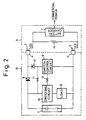
- Figure 2 shows a charge circuit including an over-discharge protection circuit according to the present invention.
- Reference numbers 1 to 8 are given to the same elements as shown in Fig. 1, and reference numbers 9 to 14 represent new elements according to the present invention.
- Reference number 9 represents a switch control circuit, 10 a switching circuit, 11 a second resistor, 12 a third resistor, 13 a diode, and 14 a first resistor.
- the first resistor 14 is connected across the battery charger 1 in the body A, and the switching circuit 10 is connected between the load 8 and the battery 7.
- the switch control circuit 9 is connected to the switching circuit 10 through the third resistor 12 and the second resistor 11.
- the diode 13 is connected to the switch control circuit 9 and the first resistor 14.
- the over-discharge protection circuit according to the present invention is constituted by the switch control circuit 9, the switching circuit 10, the first resistor 14, the second resistor 11, the third resistor 12, and the diode 13.
- the battery 7 is charged by the battery charger 1 through the charging terminals 2 and 3, the terminals 4 and 5, and the diode 6 when the handset B is placed on the body A.
- the activation of the switch control circuit 9 is based on the current flow through the diode 6 and the second resistor 11, and accordingly, the switching circuit 10 can be turned ON/OFF by the switch control circuit 9.
- the switching circuit 10 is turned ON when the battery is being charged.
- the switching circuit 10 is automatically turned OFF by the switch control circuit 9, as briefly explained below. Namely, when the voltage across the charging terminals 2 and 3 (i.e. terminals 4 and 5) becomes zero volt, the switch control circuit 9 is inactivated and the discharge current from the battery 7 flows through the second resistor 11, the diode 13, the terminal 4, the charging terminal 2, and the first resistor 14. In this case, the discharge current is very small because the resistance value of the resistor 11 is very large. Accordingly, when the switching circuit 10 is automatically turned OFF, a large discharge current does not flow to the load 8.
- the battery 7 is discharged to the load 8 and the voltage of the battery 7 is gradually lowered, and thus the voltage of the battery 7 is depleted to a level at which the telephone cannot be used, but in the present invention, since the current flow from the battery 7 to the load 8 is cut when the commercial power is accidentally turned OFF, such an over-discharge of the battery 7 is prevented.
- Figure 3 is an over-discharge protection circuit according to an embodiment of the present invention.
- the switch control circuit 9 is constituted by two transistors 9a and 9b forming a Darlington connection.
- the Darlington connection is advantageous for obtaining a large current (the current amplification factor is doubled), and accordingly, the current flowing through the resistor 11 can be set to a very small value; i.e., the resistance value of the resistor 11 can be set to a very large value.
- a collector of the transistor 9a is connected to a collector of the transistor 9b, and an emitter of the transistor 9a is connected to a base of the transistor 9b.
- the base of the transistor 9a is connected to an emitter of the transistor 10a through the second resistor 11.
- the switching circuit 10 is constituted by a PNP type transistor 10a.
- the emitter of the transistor 10a is connected to a common contact point between the battery 7, the second resistor 11, and the diode 6, the collector of the transistor 10a is connected to the load 8, and the base of the transistor 10a is connected to the collectors of the transistors 9a and 9b through the third resistor 12.
- the diode 13 is turned ON when the voltage of an anode is higher than that of a cathode of the diode 13, and therefore, the diode 13 is turned ON when the power source is accidentally turned OFF.
- the first resistor 14 detects current flowing from the battery 7 to the first resistor 14 through the second resistor 11, the diode 13, the terminal 4, and the charging terminal 2 when the power source is turned OFF.
- This resistor 14 must be provided for a half-wave rectifier circuit (not shown) of the battery charger, because an output impedance of the half-wave rectifier circuit is very large. Conversely, in a full-wave rectifier circuit (not shown), the resistor 14 is not necessary because the output impedance is smaller.
- the charging current flows to the battery 7 through the charging terminal 2, the terminal 4, and the diode 6.
- the charging current also flows to the base of the transistor 9a, and thus the transistor 9a is turned ON. In this case, the current does not flow to the diode 13 because the voltage of the cathode is equal to that of the anode.
- the transistor 9a is turned ON, the transistor 9b is also turned ON and a large current flows to the base of the transistor 10a through the third resistor 12, and accordingly, the transistor 10a is turned ON. Therefore, the charging current also flows to the load 8 during a charge of the battery 7.
- the charging of the battery 7 is continued until the voltage of the battery is equal to that of the battery charger 1.
- the diode 13 When the power source is accidentally turned OFF while the battery 7 is being charged, the diode 13 is turned ON because the voltage of the battery charger 1 is reduced to zero volt. Accordingly, the current from the battery 7 flows to the first resistor 14 through the second resistor 11 and the diode 13.
- the resistance value of the resistor 11 is larger than that of the resistor 14; i.e., the relationship between these resistors is expressed as R14 « R11.
- the resistance value of the resistor 11 is 470 K ⁇ and the resistance value of the resistor 14 is 2.2 K ⁇ as the best mode.
- the current flowing through the resistor 11 is very small (approximately, 10 ⁇ A) and the base current is also very small (approximately, 5 ⁇ A), and thus the transistor 9a can not be turned ON.
- the transistor 10a is turned OFF and the load 8 can be automatically disconnected from the battery 7 when the power source is accidentally turned OFF while the battery 7 is being charged, and thus an over-discharge of the battery 7 is prevented.
- FIG. 4 shows an over-discharge protection circuit according to another embodiment of the present invention.
- reference number 9c represents a comparator circuit
- V ref represents a reference voltage.
- the reference voltage V ref is set to a value lower than the voltage of the battery 7, and accordingly, the comparator 9c is turned ON while the battery 7 is being charged, and thus the transistor 10a is also turned ON. If the power source is accidentally turned OFF, the comparator 9c is turned OFF, since the input voltage of the comparator 9c becomes lower than the reference voltage V ref , and accordingly, the transistor 10a is turned OFF because a current is not supplied from the comparator 9c.
- the other operations are the same as those of the circuit shown in Fig. 3, and thus an explanation thereof is omitted.
Landscapes
- Engineering & Computer Science (AREA)
- Power Engineering (AREA)
- Charge And Discharge Circuits For Batteries Or The Like (AREA)
- Emergency Protection Circuit Devices (AREA)
- Electrical Discharge Machining, Electrochemical Machining, And Combined Machining (AREA)
- Mobile Radio Communication Systems (AREA)
- Amplifiers (AREA)
- Protection Of Static Devices (AREA)
Claims (4)
- Überentladungschutzschaltung beinhaltet in einer Ladeschaltung in einer tragbaren Vorrichtung mit einem tragbaren Abschnitt (B) und einem Hauptteil (A), wobei der tragbare Abschnitt und der Hauptteil verbunden sind über zwei Ladeanschlüsse (2,3) des Hauptteils bzw. zwei Ladeanschlüsse (4,5) des tragbaren Abschnitts, wenn der tragbare Abschnitt auf dem Hauptteil plaziert ist, welche umfaßt:
eine Schalteinrichtung (10) zum Verbinden und Entkoppeln einer Last (8) von einer Batterie (7), von der ein Anschluß verbunden ist mit der Batterie und deren anderer Anschluß verbunden ist mit der Last, wobei die Batterie geladen wird durch einen Batterielader (1) vorgesehen in dem Hauptteil; und
eine Schaltsteuereinrichtung (9; 9a, 9b; 9c;) verbunden mit der Schalteinrichtung (10) durch einen Widerstand (12) zum Ein- und Ausschalten der Schalteinrichtung;
dadurch gekennzeichnet daß- eine Reihenschaltung beinhaltend einen ersten und zweiten Widerstand (14,11) und eine Diode (13) vorgesehen ist, welche verbunden ist zwischen dem batterieseitigen Anschluß der Schalteinrichtung (10), wobei der andere Batterieanschluß mit der Last verbunden ist,- der erste Widerstand (14) vorgesehen ist in dem Hauptteil (A) und angeschlossen ist über dem Batterielader (1),- der zweite Widerstand (11) und die Diode (13) vorgesehen sind in dem tragbaren Abschnitt (B), elektrisch parallel zu einer Diode (6), welche einen Teil des Batterieladeweges bildet,- der zweite Widerstand (11) einen Widerstandswert hat, welcher viel größer ist als der des ersten Widerstands, und angeschlossen ist zwischen der Schalteinrichtung der Schaltsteuereinrichtung zum Steuern eines Stromflusses an die Schaltsteuereinrichtung (9), und- die Diode (13) der Reihenschaltung angeschlossen ist zwischen der Schaltsteuereinrichtung (9) und dem ersten Widerstand (14), um so zu erlauben, daß ein Fluß des Entladestroms durch den zweiten Widerstand (11) und Diode (13) an den ersten Widerstand (14) erfaßt wird, wenn die Leistungsquelle des Batterieladers zufällig ausgeschaltet ist während eines Ladens der Batterie (7), und um zu veranlassen, daß die Schaltsteuereinrichtung (9) die Schalteinrichtung (10) öffnet. - Überentladungsschutzschaltung nach Anspruch 1 dadurch gekennzeichnet daß die Schalteinrichtung einen PNP-Typ Transistor (10a) umfaßt.
- Überentladungsschutzschaltung nach Anspruch 1 oder 2, dadurch gekennzeichnet, daß die Schaltsteuereinrichtung zwei Transistoren (9a, 9b) umfaßt, welche eine Darlington Schaltung bilden.
- Überentladungsschutzschaltung nach Anspruch 1 oder 2, dadurch gekennzeichnet, daß die Schaltsteuereinrichtung einen Komparator (9c) umfaßt.
Priority Applications (1)
| Application Number | Priority Date | Filing Date | Title |
|---|---|---|---|
| AT88120149T ATE102763T1 (de) | 1987-12-03 | 1988-12-02 | Ueber-entladungsschutzschaltung. |
Applications Claiming Priority (2)
| Application Number | Priority Date | Filing Date | Title |
|---|---|---|---|
| JP62304419A JPH01148029A (ja) | 1987-12-03 | 1987-12-03 | 充電遮断時における過放電保護方式 |
| JP304419/87 | 1987-12-03 |
Publications (3)
| Publication Number | Publication Date |
|---|---|
| EP0319020A2 EP0319020A2 (de) | 1989-06-07 |
| EP0319020A3 EP0319020A3 (en) | 1990-12-05 |
| EP0319020B1 true EP0319020B1 (de) | 1994-03-09 |
Family
ID=17932772
Family Applications (1)
| Application Number | Title | Priority Date | Filing Date |
|---|---|---|---|
| EP88120149A Expired - Lifetime EP0319020B1 (de) | 1987-12-03 | 1988-12-02 | Über-Entladungsschutzschaltung |
Country Status (5)
| Country | Link |
|---|---|
| US (1) | US5177426A (de) |
| EP (1) | EP0319020B1 (de) |
| JP (1) | JPH01148029A (de) |
| AT (1) | ATE102763T1 (de) |
| DE (1) | DE3888303T2 (de) |
Cited By (3)
| Publication number | Priority date | Publication date | Assignee | Title |
|---|---|---|---|---|
| US5581170A (en) | 1994-12-12 | 1996-12-03 | Unitrode Corporation | Battery protector |
| US5652501A (en) | 1994-12-12 | 1997-07-29 | Unitrode Corporation | Voltage sensor for detecting cell voltages |
| CN102195270A (zh) * | 2011-05-31 | 2011-09-21 | 无锡新纬电池有限公司 | 软壳锂电池过充与过热报警保护结构 |
Families Citing this family (32)
| Publication number | Priority date | Publication date | Assignee | Title |
|---|---|---|---|---|
| JP3136677B2 (ja) * | 1991-07-31 | 2001-02-19 | ソニー株式会社 | 2次電池の過充電及び過放電防止回路 |
| JPH04331425A (ja) * | 1991-04-26 | 1992-11-19 | Sony Corp | 過充電防止装置、過放電防止装置、過充電・過放電防止装置、プリント基板並びにバッテリーパック |
| US5547775A (en) * | 1991-04-26 | 1996-08-20 | Sony Corporation | Circuit for preventing overcharge and overdischarge of secondary batteries |
| KR960007923Y1 (ko) * | 1991-09-18 | 1996-09-18 | 삼성전자 주식회사 | 건전지 보호회로 |
| US5334925A (en) * | 1992-09-18 | 1994-08-02 | Kendrick Robert A | Nickel cadmium battery deep cycler device |
| JP3219524B2 (ja) * | 1993-01-19 | 2001-10-15 | 三洋電機株式会社 | 二次電池の過放電保護回路 |
| JP3222999B2 (ja) * | 1993-08-20 | 2001-10-29 | 三洋電機株式会社 | 二次電池の過放電防止回路 |
| FR2721766B1 (fr) * | 1994-06-28 | 1996-07-26 | Thomson Consumer Electronics | Appareil électronique à deux modes d'alimentation. |
| JP3610595B2 (ja) * | 1994-07-20 | 2005-01-12 | 松下電器産業株式会社 | コードレス電話装置 |
| US5462814A (en) * | 1994-12-27 | 1995-10-31 | Motorola, Inc. | Method and apparatus for providing an electronic lockout for a rechargeable battery |
| US5625273A (en) * | 1994-12-30 | 1997-04-29 | Bren-Tronics Inc. | Battery safety device |
| JP3309266B2 (ja) * | 1995-02-28 | 2002-07-29 | 京セラ株式会社 | 電池パックの充電端子短絡防止回路 |
| US5668462A (en) | 1995-05-08 | 1997-09-16 | Telefonaktiebolaget Lm Ericsson | Method and apparatus for controlling a charging current of a battery in a portable chargeable electronic unit |
| US5635821A (en) * | 1995-06-30 | 1997-06-03 | National Semiconductor Corporation | Low cell charge enable circuit |
| KR980006710A (ko) * | 1996-06-29 | 1998-03-30 | 김광호 | 메모리 효과 방지를 위한 배터리 충전기 |
| KR100193736B1 (ko) * | 1996-09-17 | 1999-06-15 | 윤종용 | 배터리 보호 기능을 갖는 배터리 팩 |
| US6091948A (en) * | 1997-02-28 | 2000-07-18 | Oki Telecom, Inc. | One number service using mobile assisted call forwarding facilities |
| US6188888B1 (en) | 1998-03-30 | 2001-02-13 | Oki Telecom, Inc. | Charging unit and wireless telephone having multi-number call forwarding capability |
| US6331763B1 (en) | 1998-04-15 | 2001-12-18 | Tyco Electronics Corporation | Devices and methods for protection of rechargeable elements |
| US6034504A (en) * | 1998-06-10 | 2000-03-07 | Ericsson Inc. | Two-wire multi-rate battery charger |
| JP2000069520A (ja) * | 1998-08-26 | 2000-03-03 | Matsushita Electric Ind Co Ltd | 無線呼出受信機 |
| JP2003219009A (ja) * | 2002-01-21 | 2003-07-31 | Shijin Kogyo Sakushinkai | 無線携帯装置に串接された緊急電力供給装置 |
| US7789685B2 (en) * | 2006-12-18 | 2010-09-07 | Caterpillar Inc | Electrical shorting system |
| US7616421B2 (en) * | 2006-12-18 | 2009-11-10 | Caterpillar Inc. | Electrical interface system |
| CN101557119B (zh) * | 2008-04-09 | 2012-11-21 | 鹏智科技(深圳)有限公司 | 二次电池的充电控制电路 |
| US8022661B1 (en) | 2008-04-28 | 2011-09-20 | Lockheed Martin Corporation | Battery over-discharge protection with dead-bus recovery |
| US8250385B2 (en) * | 2009-01-30 | 2012-08-21 | Hewlett-Packard Development Company, L.P. | Method and system of dissipating power from a power supply |
| JP5803446B2 (ja) * | 2011-09-02 | 2015-11-04 | ミツミ電機株式会社 | 半導体集積回路、保護回路及び電池パック |
| ITMI20120333A1 (it) * | 2012-03-02 | 2013-09-03 | St Microelectronics Srl | Caricatore di batterie. |
| US9041357B2 (en) | 2012-04-23 | 2015-05-26 | Motorola Solutions, Inc. | Apparatus for minimizing self-discharge of a smart battery pack |
| CN104868449B (zh) * | 2014-06-30 | 2017-11-03 | 北汽福田汽车股份有限公司 | 一种电池单体过放保护方法及系统 |
| US10992144B2 (en) * | 2017-05-17 | 2021-04-27 | Galley Power LLC | Battery balancing and current control with bypass circuit for load switch |
Family Cites Families (9)
| Publication number | Priority date | Publication date | Assignee | Title |
|---|---|---|---|---|
| US3766403A (en) * | 1970-05-26 | 1973-10-16 | Matsushita Electric Industrial Co Ltd | Apparatus for ensuring dc power supply from either ac or rechargeable dc source |
| DE2128015B1 (de) * | 1971-06-05 | 1972-10-05 | Friemann & Wolf Gmbh | Schaltungsanordnung zum Schutz vor Tiefentladung eines Akkumulators in einem von einem Ladegerät aufladbaren Notstromversorgungsgerät |
| DE2362107C3 (de) * | 1973-12-14 | 1979-09-20 | Gebr. Eickhoff, Maschinenfabrik U. Eisengiesserei Mbh, 4630 Bochum | Stromversorgungseinrichtung fUr eine Gewinnungsmaschine, insbesondere für eine Walzenschrämmaschine |
| GB2010028B (en) * | 1977-11-04 | 1982-04-28 | Minitronics Pty Ltd | Control of power supply |
| CH627983A5 (it) * | 1978-08-21 | 1982-02-15 | Gilardoni Angelo | Impianto di illuminazione di un ciclo. |
| JPS57122956U (de) * | 1981-01-23 | 1982-07-31 | ||
| US4536695A (en) * | 1983-12-12 | 1985-08-20 | Lin Ming Hsin | Discharging protection device for battery-operated portable electric light |
| JPS6281133A (ja) * | 1985-10-03 | 1987-04-14 | Nippon Telegr & Teleph Corp <Ntt> | 無線電話装置の連続送信禁止方式 |
| JPS63248227A (ja) * | 1987-04-03 | 1988-10-14 | Aisin Seiki Co Ltd | 電話装置 |
-
1987
- 1987-12-03 JP JP62304419A patent/JPH01148029A/ja active Pending
-
1988
- 1988-12-02 DE DE3888303T patent/DE3888303T2/de not_active Expired - Fee Related
- 1988-12-02 AT AT88120149T patent/ATE102763T1/de not_active IP Right Cessation
- 1988-12-02 US US07/279,108 patent/US5177426A/en not_active Expired - Fee Related
- 1988-12-02 EP EP88120149A patent/EP0319020B1/de not_active Expired - Lifetime
Cited By (3)
| Publication number | Priority date | Publication date | Assignee | Title |
|---|---|---|---|---|
| US5581170A (en) | 1994-12-12 | 1996-12-03 | Unitrode Corporation | Battery protector |
| US5652501A (en) | 1994-12-12 | 1997-07-29 | Unitrode Corporation | Voltage sensor for detecting cell voltages |
| CN102195270A (zh) * | 2011-05-31 | 2011-09-21 | 无锡新纬电池有限公司 | 软壳锂电池过充与过热报警保护结构 |
Also Published As
| Publication number | Publication date |
|---|---|
| EP0319020A2 (de) | 1989-06-07 |
| US5177426A (en) | 1993-01-05 |
| ATE102763T1 (de) | 1994-03-15 |
| DE3888303D1 (de) | 1994-04-14 |
| JPH01148029A (ja) | 1989-06-09 |
| EP0319020A3 (en) | 1990-12-05 |
| DE3888303T2 (de) | 1994-08-04 |
Similar Documents
| Publication | Publication Date | Title |
|---|---|---|
| US5177426A (en) | Over-discharge protection circuitry | |
| US4458111A (en) | Charging and discharging circuit | |
| KR100415763B1 (ko) | 2차 전지팩 | |
| EP0406858B1 (de) | Batterielader und Verfahren für ein schnurloses tragbares Telefongerät mit einer Einrichtung zum Erhaltungsladen der batterie mit einem erhöhten Strom während der Stand-by-Periode des Telefongerätes | |
| US5578875A (en) | Dual battery recharger with backup power feature for use in systems having a base unit and battery-powered portable unit | |
| EP0621649B1 (de) | Batteriepack | |
| KR100549813B1 (ko) | 충전제어방법 및 충전제어장치 | |
| US6794851B2 (en) | Charging circuit and battery charger | |
| US5867798A (en) | Cordless telephone system having power interruption detection | |
| US5576611A (en) | Battery charging system | |
| US5920180A (en) | Battery charger for preventing memory effect | |
| EP0580180B1 (de) | Ladeschaltung geeignet für die direkte Gleichspannungsversorgung einer Stromversorgungseinheit bei einem Batteriewechsel | |
| US5438252A (en) | Power supply control module for a battery control system of an appliance, and a battery equipped with such a module | |
| EP0720305A2 (de) | Tragbares Telefon | |
| JP3358559B2 (ja) | 低電力消費回路及び二次電池保護回路 | |
| US5530296A (en) | Power supply switching apparatus | |
| US5825157A (en) | Camera using solar battery | |
| KR0184506B1 (ko) | 충전용 배터리의 과방전 방지회로 | |
| JPH1012283A (ja) | バツテリパツク及びバツテリパツクの制御方法 | |
| US20030102843A1 (en) | Charger and electrical apparatus | |
| KR0126190Y1 (ko) | 휴대폰에서 전원제어장치 | |
| JP2546098Y2 (ja) | 充電回路 | |
| JP2003164070A (ja) | 充電器 | |
| JPH0799730A (ja) | 充放電装置 | |
| KR0134936B1 (ko) | 무선전화기 휴대장치의 과방전 방지회로 |
Legal Events
| Date | Code | Title | Description |
|---|---|---|---|
| PUAI | Public reference made under article 153(3) epc to a published international application that has entered the european phase |
Free format text: ORIGINAL CODE: 0009012 |
|
| AK | Designated contracting states |
Kind code of ref document: A2 Designated state(s): AT CH DE LI NL SE |
|
| PUAL | Search report despatched |
Free format text: ORIGINAL CODE: 0009013 |
|
| AK | Designated contracting states |
Kind code of ref document: A3 Designated state(s): AT CH DE LI NL SE |
|
| 17P | Request for examination filed |
Effective date: 19901220 |
|
| 17Q | First examination report despatched |
Effective date: 19920923 |
|
| GRAA | (expected) grant |
Free format text: ORIGINAL CODE: 0009210 |
|
| AK | Designated contracting states |
Kind code of ref document: B1 Designated state(s): AT CH DE LI NL SE |
|
| PG25 | Lapsed in a contracting state [announced via postgrant information from national office to epo] |
Ref country code: AT Effective date: 19940309 |
|
| REF | Corresponds to: |
Ref document number: 102763 Country of ref document: AT Date of ref document: 19940315 Kind code of ref document: T |
|
| REF | Corresponds to: |
Ref document number: 3888303 Country of ref document: DE Date of ref document: 19940414 |
|
| PLBE | No opposition filed within time limit |
Free format text: ORIGINAL CODE: 0009261 |
|
| STAA | Information on the status of an ep patent application or granted ep patent |
Free format text: STATUS: NO OPPOSITION FILED WITHIN TIME LIMIT |
|
| EAL | Se: european patent in force in sweden |
Ref document number: 88120149.5 |
|
| 26N | No opposition filed | ||
| PGFP | Annual fee paid to national office [announced via postgrant information from national office to epo] |
Ref country code: DE Payment date: 19951214 Year of fee payment: 8 |
|
| PGFP | Annual fee paid to national office [announced via postgrant information from national office to epo] |
Ref country code: SE Payment date: 19951215 Year of fee payment: 8 |
|
| PGFP | Annual fee paid to national office [announced via postgrant information from national office to epo] |
Ref country code: CH Payment date: 19951229 Year of fee payment: 8 |
|
| PGFP | Annual fee paid to national office [announced via postgrant information from national office to epo] |
Ref country code: NL Payment date: 19951230 Year of fee payment: 8 |
|
| PG25 | Lapsed in a contracting state [announced via postgrant information from national office to epo] |
Ref country code: SE Effective date: 19961203 |
|
| PG25 | Lapsed in a contracting state [announced via postgrant information from national office to epo] |
Ref country code: LI Effective date: 19961231 Ref country code: CH Effective date: 19961231 |
|
| PG25 | Lapsed in a contracting state [announced via postgrant information from national office to epo] |
Ref country code: NL Effective date: 19970701 |
|
| REG | Reference to a national code |
Ref country code: CH Ref legal event code: PL |
|
| NLV4 | Nl: lapsed or anulled due to non-payment of the annual fee |
Effective date: 19970701 |
|
| PG25 | Lapsed in a contracting state [announced via postgrant information from national office to epo] |
Ref country code: DE Effective date: 19970902 |
|
| EUG | Se: european patent has lapsed |
Ref document number: 88120149.5 |