EP0319352A1 - Apparat zum Ablesen eines Zählers - Google Patents
Apparat zum Ablesen eines Zählers Download PDFInfo
- Publication number
- EP0319352A1 EP0319352A1 EP88311519A EP88311519A EP0319352A1 EP 0319352 A1 EP0319352 A1 EP 0319352A1 EP 88311519 A EP88311519 A EP 88311519A EP 88311519 A EP88311519 A EP 88311519A EP 0319352 A1 EP0319352 A1 EP 0319352A1
- Authority
- EP
- European Patent Office
- Prior art keywords
- output
- contacts
- test
- wiper
- measurement
- Prior art date
- Legal status (The legal status is an assumption and is not a legal conclusion. Google has not performed a legal analysis and makes no representation as to the accuracy of the status listed.)
- Pending
Links
Images



Classifications
-
- G—PHYSICS
- G06—COMPUTING OR CALCULATING; COUNTING
- G06M—COUNTING MECHANISMS; COUNTING OF OBJECTS NOT OTHERWISE PROVIDED FOR
- G06M3/00—Counters with additional facilities
- G06M3/06—Counters with additional facilities for printing or separately displaying result of count
-
- G—PHYSICS
- G06—COMPUTING OR CALCULATING; COUNTING
- G06M—COUNTING MECHANISMS; COUNTING OF OBJECTS NOT OTHERWISE PROVIDED FOR
- G06M1/00—Design features of general application
- G06M1/27—Design features of general application for representing the result of count in the form of electric signals, e.g. by sensing markings on the counter drum
- G06M1/276—Design features of general application for representing the result of count in the form of electric signals, e.g. by sensing markings on the counter drum using mechanically-actuated contacts
Definitions
- This invention relates to metering apparatus and in the most important example to apparatus for metering usage of public utilities such as gas and water.
- a wiper contact on each number wheel makes contact successively with an array of position contacts.
- By applying appropriate electrical signals to the wiper contacts and monitoring the signals appearing on the position contacts it is possible to provide an electrical output representative of the number wheel positions.
- utility metering apparatus is required to operate substantially continuously without maintenance over extremely long periods of time. Because of wear or corrosion, mechanical faults may occasionally arise in the contact structures. Such faults will not necessarily prevent operation of the apparatus but will often result in erroneous electrical indications of the meter reading.
- spreading of contacts through wear, or the deposition of conducting material between contacts can lead to short circuiting of two or more adjacent position contacts. Such short circuiting can lead to significant errors in the meter reading. Whilst the likelihood of a fault arising on any particular meter is small, the potentially large number of meters to be included in a utility billing system and the significance of any error in the amount billed for utility usage, means that this problem demands careful attention.
- the present invention consists in metering apparatus comprising a metering device having an output; a plurality of indicator elements driven in response to the meter output such that the orientation of the respective indicator elements is indicative of the meter output; for each indicator element an array of position contacts, corresponding position contacts from each said array being connected with a corresponding one of a plurality of position terminals, and a wiper contact disposed to make contact successively with the position contacts of the array on driving of the corresponding indicator element; generator means for applying, in a measurement mode, measurement signals in sequence to the wiper contacts and for applying, in a test mode alternating with the measurement mode, test signals in sequence to the position terminals; encoder means connected with the position terminals and adapted to provide an encoded output representative of the signals on said position terminals; and data output means arranged to receive said encoded output and adapted, in synchronism with operation of the generator means, to provide a data output, said data representing in the measurement mode the position of the respective indicator elements and, in the test mode, a test
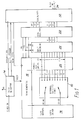
- block 10 schematically represets a number wheel contact array and of serial number links.
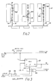
- a bank of six number wheels is assumed with, as shown in Figure 2, each number wheel 12 having a wiper contact (W1 to W6).
- a main circuit board 14 carries three contact boards 16 which are interposed between corresponding pairs of number wheels.
- Each contact board carries on both sides an array of ten circumferentially disposed position contacts 18.
- Corresponding position contacts from each array are connected together through tracks on the circuit boards and communicate with a corresponding one of ten position terminals (D0 to D9).
- D0 to D9 corresponding one of ten position terminals
- the metering apparatus additionally comprises eight serial contacts (S1 to S8) which (in a manner not apparent from Figure 2) are connected through fixed links to a particular one of the position terminals D0 to D9. These links are set at the time of assembly of the metering apparatus and enable the definition of a unique serial number for each product.
- the main circuit board 14 additionally carries the integrated circuits and other components embodying the electronic circuitry of Figure 1.
- a scan generator 16 causes, through wiper drive 18, a logical LOW signal to be applied in a pre set sequence to the six wiper contacts W1 to W6 and the eight serial number contacts S1 to S8.
- An encoder which comprises an input decoding unit 20 and a code modifier unit 22, monitors the signals appearing upon the position terminals D0 to D9 at each point in this sequence and provides an encoded signal in parallel form to the serialiser 12.
- This parallel input is scanned in synchronism with the application of logic signals to the wiper and serial number contacts and a serial ASCII output is produced at output terminal 24.
- This ASCII output includes six characters representing the positions of the six number wheels and eight characters representing the unique serial number.
- a forced input unit 26 interposed between the position terminals D0 to D9 and the input decoding unit 20 is operative during validation modes - which alternate with these measurement modes - to provide validation of the electrical contact integrity.
- the clock generator 14 comprises a divider 50 (4040), inverters 52, 54 and 56; AND gate 58 and OR gate 60.
- the external clock input at 1,200 pulses per second is supplied through inverter 52 to the clock input of divider 50 and also to a SYSTEM CLOCK LINE which is connected with the serialiser 12.
- the 24 output of the divider is AND'ed in gate 58 with the 29 output inverted in inverter 54, to produce a TRIGGER output which comprises sixteen trigger pulses, each corresponding with sixteen SYSTEM CLOCK pulses, followed by a gap equivalent in time to sixteen trigger pulses.
- line a) illustrates the TRIGGER output with line d) illustrating - to a considerably enlarged scale - one period of the TRIGGER output.
- the remaining lines of Figure 9 correspond to the time scale of line d); thus line b) shows the sixteen SYSTEM CLOCK pulses occuring within a single trigger output period.
- the 29 output of divider 50, through inverters 54 and 56, is OR'ed in gate 60 with a manual reset (MR), input which is connected additionally with the divider 50 and with the serialiser unit 12.
- MR manual reset
- the serialiser unit 12 comprises a decade counter 62 (4017) which receives as a clock input the SYSTEM CLOCK line.
- the decade counter 62 additionally receives the MR line through OR gate 64.
- OR gate 64 Of the ten output lines of counter 62, only ines Q0, Q1 and Q9 are utilised.
- Line Q0 serves through inverter 66 to produce a SCAN CLOCK signal which is illustrated at line f) of the Figure 9 timing diagram.
- the scan generator 16 receives the SCAN CLOCK line as the clock input to a counter 70 (4520).
- Counter 70 provides a binary output on lines 20, 21, 22 and 23 which are connected to corresponding inputs of two three to eight line converters 72 and 74 (HC 138). Enabled alternately by the 23 output of counter 70, these two converters (as will well be understood by those skilled in the art) operate as a four to sixteen line converter of the counter output.
- the sixteen output lines are labelled Y0 to Y15.
- Negative logic is employed, and activation comprises the pulling LOW of the corresponding scan generator output Y0 to Y15.
- the scan generator 16 additionally comprises a flip flop 76 driven by the 23 output of counter 70 through inverter 78. The flip flop 76 provides PQ and PQ outputs.
- scan generator Y0 is LOW and all other generator outputs are HIGH.
- the PQ flag is LOW.
- the generator outputs are pulled LOW in sequence.
- the PQ flag goes HIGH and the scan generator outputs Y0 to Y15 are again pulled LOW in sequence.
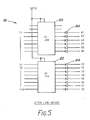
- the wiper driver 18 comprises two octal buffers 80 and 82 (HC 244) which both receive the PQ line as an enabling input and receive between them the scan generator outputs Y1 to Y14.
- Scan generator outputs Y0 and Y15 are not required in the scanning of six wiper contacts and eight serial number links and are used, as we will describe, to generate fixed ASCII character identifiers.
- a LOW signal of scan generator output Y1 will result in wiper contact W1 being pulled LOW.
- PQ HIGH, the buffers are disabled and all output transistors are turned off. All the buffer outputs are therefore high impedance and the wiper contacts and the serial number links are effectively permitted to float.
- a diode 84 is provided on each output line of the buffers 80 and 82 so as to prevent interaction between adjacent lines.
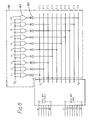
- each of these connecting lines is additionally connected through a diode 90 with one of a series of OR gates 92.
- Each OR gate 92 receives as one input the PQ signal from inverter 94 and as the other input the corresponding one of the scan generator outputs Y1 to Y10.
- the code modifier unit 20 comprises a high priority encoder 102 (HC147). This has 20, 21, 22 and 23 outputs which provide a binary indication of, in the measurement mode, the position or value of the number wheel or serial link currently being scanned and. in the mechanics validation mode, an effective numerical value created by the forced inputs.
- the outputs from encoder 102 are connected with respective AND gates 104, second inputs of which are connected with an inverter 106. This is connected in turn with the output of a NOR gate 108 receiving the outputs of two NAND gates 110. These NAND gates receive as inputs the same signals applied to inputs D′0 to D′9 of the encoder 102.
- the function of the gates 106, 108 and 110 is to detect the "all contacts open-circuit" condition and, through AND gates 104, effectively disable the encoder in those circumstances.
- the outputs of the AND gates are connected with the inputs of respective NOR gates 108, with the other inputs of each NOR gate being connected to the output of a NAND gate 110 receiving Y0 and Y15 as inputs.
- Y0 and Y15 are both HIGH (which will be the case during scanning of the six wiper contacts and eight serial number links as lines Y1 to Y14 are successively pulled LOW).
- the input decoding unit 20 will provide a binary coded decimal output to the code modifier unit 22. If either of Y0 or Y15 is LOW, the outputs of NOR gates 108 are pulled LOW, effectively disabling the input decoder.
- the code modifier unit 22 is also shown in Figure 7. It receives the parallel output lines from the input decoding unit 20 together with Y0, Y15, PQ and PQ. The code modifier unit 22 provides an output on six parallel lines to the serialiser 12. Referring both to Figure 7 and the truth table which is Figure 10, it will be apparent that if both Y0 and Y15 are HIGH (that is to say during scanning of the wiper contacts and serial number links), the output from the input decoder is passed directly to the serialising unit 12 and appears as an ASCII numerical character 0 to 9.
- the code modifier serves the purpose of inserting code for an appropriate ASCII character at the beginning and end of each sixteen pulse sequence.
- the serialiser 12 comprises an eight bit parallel to serial converter 120 (4014). This receives as inputs the six output lines from the code modifier unit 22, the line Y0 and a parity line generated in parity generator 22 and gated by and gate 124. As illustrated schematically in Figure 8, the parity generator 122 receives the other inputs to the parallel to serial converter. AND gate 124 additionally receives line Q1 from decade counter 62. The converter 120 further receives as a clock input the SYSTEM CLOCK line and as a parallel/serial load flag the output of the NOR gate 126. The inputs to this NOR gate 126 are, respectively, the SCAN CLOCK line and the output of a latch formed by paired NOR gates 128 and 130 receiving as respective inputs the TRIGGER line and output Q9 from the decade counter 62.
- output Q0 is HIGH so that converter 120 is in a parallel load mode and eight bits are loaded. These comprise a start bit (corresponding to the permanently high connection of the first input terminal to the converter 120).
- the converter is switched to serial load so that, whilst Q1 is LOW, parity data is clocked in (see Figure 9j).
- gate 124 effectively isolates the parity generator so that zeros are clocked in, in series. The first of these zeros is technically a stop bit.
- the serial output is illustrated at Figure 9c).
- N1 to N6 represent numeric characters indicating the position of the six number wheels and, similarly, S1 to S8 are numeric characters providing the unique serial number.
- the characters 0 to 9 in the second pulse sequence arise directly from the input forcing of the test or mechanics validation mode.
- the question mark characters represent an open circuit condition on all contacts.
- the scan signal Y4 will, in the forced input operation of the test mode, cause a LOW to appear not only on input D′4 of the input decoding unit 20, but also on input D′5, via the mechanical short circuit. Since the input decoder operates on higher value expected "4". In this case, the 16 character ASCII in the test mode would be:- M0123556789????[CR]
- FIG 11 there is shown diagramatically an interface for use with the encoding circuitry described above.
- the function of this interface is to take power from a portable reading device held in proximity to the interface and to transmit data to the device on demand.
- the interface includes power and data coils L1 and L2 respectively. These are mounted at a suitable location to enable a probe or other part of the reading unit to be positioned with corresponding coils in the probe being inductively linked with the coils L1 and L2 as shown schematically in the drawing.
- Coil L1 feeds a power supply unit 200 which in generally conventional manner is provided with a rectifying bridge network, smoothing capacitors and voltage protection Zener diodes.
- the power supply unit 200 has a rectified but unregulated output on line 202; a rectified and regulated output on line 204 and an alternating output f in .
- This alternating output is applied as a clock input to a multiplexer 206 which has an output switched at the frequency f in between the regulated supply rail 204 and ground.
- the output of multiplexer 206 is connected to a binary divider 208.
- Output line 2 x of the divider is connected as a clock input to a further multiplexer 210 which has inputs connected respectively with output 2 y of divider 208 and the regulated supply rail 204.
- the output of the multiplexer 210 is switched between the supply rail and the output 2 y at a frequency corresponding to the output 2 x .
- an appropriate mark space ratio is created.
- the output of multiplexer 210 is connected with a driver stage 212 providing on terminal pair T1 both the clock input and power to the previously described encoder circuitry.
- the output from the serialiser 12 is connected on terminal paid T2 as the clock input to a further multiplexer 214 having inputs which are respectively connected to the ground rail and permitted to float.
- This multiplexer accordingly functions as an inhibitor.
- the output of multiplexer 214 is connected as the control input to a Colpitts oscillator 216 with the output data coil L2 being connected across the output of the oscillator and the unregulated supply rail. There accordingly appears across the output coil L2 a modulated signal representative of the ASCII output of the above described encoder.
- block 300 designates the circuit elements of Figure 1 with the exception, of course, of the contacts and serial number links represented by block 10.
- terminal T1 The combined power and clock input on terminal T1 is rectified and smoothed through diode D1 and capacitor C1. Voltage regulation is provided by resistance R1 and Zener diode ZD1, whilst capacitor C3 serves as noise suppression. Terminal T1 is further connected through resistance R2 to the base of npn transistor TR1, resistance R4 serving in turn to connect the base of TR1 with ground. The collector of TR1 serves to provide the CLOCK input with capacitor C2 again serving as noise suppression.
- the SERIAL OUTPUT line is connected through resistance R3 with the base of npn transistor TR2, the collector of which is connected with terminal T2.
- circuit elements comprised within block 300 are embodied in a single application specific integrated circuit.
- the described interface could be replaced by alternative designs or by a permanent power supply and fixed data links. Still further interfaces could be provided for other methods of remote interrogation of the meter reading.
Landscapes
- Physics & Mathematics (AREA)
- General Physics & Mathematics (AREA)
- Engineering & Computer Science (AREA)
- Theoretical Computer Science (AREA)
- Arrangements For Transmission Of Measured Signals (AREA)
Applications Claiming Priority (2)
| Application Number | Priority Date | Filing Date | Title |
|---|---|---|---|
| GB878728359A GB8728359D0 (en) | 1987-12-04 | 1987-12-04 | Improvements in metering apparatus |
| GB8728359 | 1987-12-04 |
Publications (1)
| Publication Number | Publication Date |
|---|---|
| EP0319352A1 true EP0319352A1 (de) | 1989-06-07 |
Family
ID=10627976
Family Applications (2)
| Application Number | Title | Priority Date | Filing Date |
|---|---|---|---|
| EP88311519A Pending EP0319352A1 (de) | 1987-12-04 | 1988-12-05 | Apparat zum Ablesen eines Zählers |
| EP89900857A Withdrawn EP0345332A1 (de) | 1987-12-04 | 1988-12-05 | Apparat zum ablesen eines zählers |
Family Applications After (1)
| Application Number | Title | Priority Date | Filing Date |
|---|---|---|---|
| EP89900857A Withdrawn EP0345332A1 (de) | 1987-12-04 | 1988-12-05 | Apparat zum ablesen eines zählers |
Country Status (6)
| Country | Link |
|---|---|
| US (1) | US5045776A (de) |
| EP (2) | EP0319352A1 (de) |
| JP (1) | JPH02503125A (de) |
| AU (1) | AU615977B2 (de) |
| GB (1) | GB8728359D0 (de) |
| WO (1) | WO1989005497A1 (de) |
Families Citing this family (4)
| Publication number | Priority date | Publication date | Assignee | Title |
|---|---|---|---|---|
| IT1244205B (it) * | 1990-12-19 | 1994-07-08 | Sgs Thomson Microelectronics | Circuito di generazione di un clock di scansione in un dispositivo di analisi operativa di tipo seriale per circuito integrato |
| JP3336833B2 (ja) | 1995-10-12 | 2002-10-21 | ジェイエスアール株式会社 | アスファルト改質材 |
| US6674371B1 (en) * | 2000-08-18 | 2004-01-06 | Hersey Meter Company | Utility meter remote reader |
| US6828517B2 (en) * | 2001-05-16 | 2004-12-07 | Bourns, Inc. | Position encoder |
Citations (4)
| Publication number | Priority date | Publication date | Assignee | Title |
|---|---|---|---|---|
| FR2145142A5 (de) * | 1971-07-07 | 1973-02-16 | Gamon Calmet Ind Inc | |
| FR2174559A5 (de) * | 1972-01-21 | 1973-10-12 | Rockwell Mfg Co | |
| GB1371761A (en) * | 1972-01-14 | 1974-10-23 | Nat Res Dev | Checking of meters |
| EP0240761A1 (de) * | 1983-07-01 | 1987-10-14 | M & FC HOLDING COMPANY, INC. | Verfahren zur Gewinnung und Übertragung von Zählerdaten |
Family Cites Families (6)
| Publication number | Priority date | Publication date | Assignee | Title |
|---|---|---|---|---|
| US3641537A (en) * | 1969-04-16 | 1972-02-08 | Westinghouse Electric Corp | Metering system having a remote register |
| US3676876A (en) * | 1971-02-26 | 1972-07-11 | United Gas Industries Ltd | Meter reading units |
| US3778795A (en) * | 1972-03-13 | 1973-12-11 | Linscott | Remotely controlled automatic utility meter reader |
| US3840866A (en) * | 1973-02-08 | 1974-10-08 | Textron Inc | Meter reading |
| US4782341A (en) * | 1983-07-01 | 1988-11-01 | Rockwell International Corporation | Meter data gathering and transmission system |
| US4688038A (en) * | 1985-09-30 | 1987-08-18 | Milton S. Gerstein | Remote meter-reader device for gas meters, and the like |
-
1987
- 1987-12-04 GB GB878728359A patent/GB8728359D0/en active Pending
-
1988
- 1988-12-05 EP EP88311519A patent/EP0319352A1/de active Pending
- 1988-12-05 AU AU28211/89A patent/AU615977B2/en not_active Ceased
- 1988-12-05 EP EP89900857A patent/EP0345332A1/de not_active Withdrawn
- 1988-12-05 JP JP1500665A patent/JPH02503125A/ja active Pending
- 1988-12-05 WO PCT/GB1988/001097 patent/WO1989005497A1/en not_active Ceased
- 1988-12-05 US US07/382,645 patent/US5045776A/en not_active Expired - Fee Related
Patent Citations (4)
| Publication number | Priority date | Publication date | Assignee | Title |
|---|---|---|---|---|
| FR2145142A5 (de) * | 1971-07-07 | 1973-02-16 | Gamon Calmet Ind Inc | |
| GB1371761A (en) * | 1972-01-14 | 1974-10-23 | Nat Res Dev | Checking of meters |
| FR2174559A5 (de) * | 1972-01-21 | 1973-10-12 | Rockwell Mfg Co | |
| EP0240761A1 (de) * | 1983-07-01 | 1987-10-14 | M & FC HOLDING COMPANY, INC. | Verfahren zur Gewinnung und Übertragung von Zählerdaten |
Also Published As
| Publication number | Publication date |
|---|---|
| AU2821189A (en) | 1989-07-05 |
| GB8728359D0 (en) | 1988-01-13 |
| JPH02503125A (ja) | 1990-09-27 |
| EP0345332A1 (de) | 1989-12-13 |
| WO1989005497A1 (en) | 1989-06-15 |
| AU615977B2 (en) | 1991-10-17 |
| US5045776A (en) | 1991-09-03 |
Similar Documents
| Publication | Publication Date | Title |
|---|---|---|
| AU651582B2 (en) | Two and three wire utility data communications system | |
| US5243338A (en) | Two and three wire utility data communications system | |
| US4207557A (en) | User electric energy consumption apparatus | |
| JPH0514959B2 (de) | ||
| EP0093769B1 (de) | Speichersicherheitsystem | |
| CA1129004A (en) | Hybrid signature test method and apparatus | |
| US4103289A (en) | Calculator theft prevention device | |
| US5045776A (en) | Metering apparatus | |
| US4233590A (en) | Supplemental energy register | |
| CN201237737Y (zh) | 顺序事件记录性能测试装置 | |
| US5644222A (en) | Process for testing an electronic electricity meter | |
| US4369493A (en) | Response time monitor | |
| GB2195029A (en) | Testing electrical circuits | |
| JPS6215919B2 (de) | ||
| US3725877A (en) | Self contained memory keyboard | |
| US3920962A (en) | Pulse summing circuit | |
| US3846702A (en) | Time accumulator man-hours expended | |
| JPH0354361B2 (de) | ||
| CN109379812A (zh) | Led自动编码地址电路以及编码方法 | |
| GB2195028A (en) | Testing electrical circuits | |
| RU8136U1 (ru) | Имитатор ир-60-500 для отладки корабельных цифровых управляющих систем | |
| US3495221A (en) | Data detector | |
| GB2195027A (en) | Testing electrical circuits | |
| KR910007399B1 (ko) | 원격 검침용 데이타 전송장치 | |
| CN1117167A (zh) | 地址数据产生装置 |
Legal Events
| Date | Code | Title | Description |
|---|---|---|---|
| PUAI | Public reference made under article 153(3) epc to a published international application that has entered the european phase |
Free format text: ORIGINAL CODE: 0009012 |
|
| AK | Designated contracting states |
Kind code of ref document: A1 Designated state(s): ES GR |
|
| STAA | Information on the status of an ep patent application or granted ep patent |
Free format text: STATUS: REQUEST FOR EXAMINATION WAS MADE |
|
| 17P | Request for examination filed |
Effective date: 19890803 |
|
| RAP1 | Party data changed (applicant data changed or rights of an application transferred) |
Owner name: ABB KENT PLC |
|
| XX | Miscellaneous (additional remarks) |
Free format text: VERFAHREN ABGESCHLOSSEN INFOLGE VERBINDUNG MIT 89900857.7/0345332 (EUROPAEISCHE ANMELDENUMMER/VEROEFFENTLICHUNGSNUMMER) VOM 06.05.91. |