EP0319797B1 - Méthode et appareil pour mesurer la densité de défauts et leur distribution - Google Patents
Méthode et appareil pour mesurer la densité de défauts et leur distribution Download PDFInfo
- Publication number
- EP0319797B1 EP0319797B1 EP19880119684 EP88119684A EP0319797B1 EP 0319797 B1 EP0319797 B1 EP 0319797B1 EP 19880119684 EP19880119684 EP 19880119684 EP 88119684 A EP88119684 A EP 88119684A EP 0319797 B1 EP0319797 B1 EP 0319797B1
- Authority
- EP
- European Patent Office
- Prior art keywords
- flat surface
- image data
- defect
- images
- laser beam
- Prior art date
- Legal status (The legal status is an assumption and is not a legal conclusion. Google has not performed a legal analysis and makes no representation as to the accuracy of the status listed.)
- Expired - Lifetime
Links
Images


Classifications
-
- G—PHYSICS
- G06—COMPUTING OR CALCULATING; COUNTING
- G06T—IMAGE DATA PROCESSING OR GENERATION, IN GENERAL
- G06T7/00—Image analysis
- G06T7/0002—Inspection of images, e.g. flaw detection
- G06T7/0004—Industrial image inspection
-
- G—PHYSICS
- G01—MEASURING; TESTING
- G01N—INVESTIGATING OR ANALYSING MATERIALS BY DETERMINING THEIR CHEMICAL OR PHYSICAL PROPERTIES
- G01N21/00—Investigating or analysing materials by the use of optical means, i.e. using sub-millimetre waves, infrared, visible or ultraviolet light
- G01N21/84—Systems specially adapted for particular applications
- G01N21/88—Investigating the presence of flaws or contamination
- G01N21/95—Investigating the presence of flaws or contamination characterised by the material or shape of the object to be examined
- G01N21/9501—Semiconductor wafers
- G01N21/9505—Wafer internal defects, e.g. microcracks
-
- G—PHYSICS
- G01—MEASURING; TESTING
- G01N—INVESTIGATING OR ANALYSING MATERIALS BY DETERMINING THEIR CHEMICAL OR PHYSICAL PROPERTIES
- G01N21/00—Investigating or analysing materials by the use of optical means, i.e. using sub-millimetre waves, infrared, visible or ultraviolet light
- G01N21/17—Systems in which incident light is modified in accordance with the properties of the material investigated
- G01N2021/178—Methods for obtaining spatial resolution of the property being measured
- G01N2021/1785—Three dimensional
-
- G—PHYSICS
- G01—MEASURING; TESTING
- G01N—INVESTIGATING OR ANALYSING MATERIALS BY DETERMINING THEIR CHEMICAL OR PHYSICAL PROPERTIES
- G01N21/00—Investigating or analysing materials by the use of optical means, i.e. using sub-millimetre waves, infrared, visible or ultraviolet light
- G01N21/17—Systems in which incident light is modified in accordance with the properties of the material investigated
- G01N21/47—Scattering, i.e. diffuse reflection
- G01N2021/4735—Solid samples, e.g. paper, glass
-
- G—PHYSICS
- G01—MEASURING; TESTING
- G01N—INVESTIGATING OR ANALYSING MATERIALS BY DETERMINING THEIR CHEMICAL OR PHYSICAL PROPERTIES
- G01N21/00—Investigating or analysing materials by the use of optical means, i.e. using sub-millimetre waves, infrared, visible or ultraviolet light
- G01N21/84—Systems specially adapted for particular applications
- G01N21/88—Investigating the presence of flaws or contamination
- G01N21/8851—Scan or image signal processing specially adapted therefor, e.g. for scan signal adjustment, for detecting different kinds of defects, for compensating for structures, markings, edges
- G01N2021/8887—Scan or image signal processing specially adapted therefor, e.g. for scan signal adjustment, for detecting different kinds of defects, for compensating for structures, markings, edges based on image processing techniques
-
- G—PHYSICS
- G01—MEASURING; TESTING
- G01N—INVESTIGATING OR ANALYSING MATERIALS BY DETERMINING THEIR CHEMICAL OR PHYSICAL PROPERTIES
- G01N2201/00—Features of devices classified in G01N21/00
- G01N2201/10—Scanning
- G01N2201/102—Video camera
-
- G—PHYSICS
- G01—MEASURING; TESTING
- G01N—INVESTIGATING OR ANALYSING MATERIALS BY DETERMINING THEIR CHEMICAL OR PHYSICAL PROPERTIES
- G01N2201/00—Features of devices classified in G01N21/00
- G01N2201/10—Scanning
- G01N2201/108—Miscellaneous
- G01N2201/1087—Focussed scan beam, e.g. laser
-
- G—PHYSICS
- G06—COMPUTING OR CALCULATING; COUNTING
- G06T—IMAGE DATA PROCESSING OR GENERATION, IN GENERAL
- G06T2207/00—Indexing scheme for image analysis or image enhancement
- G06T2207/10—Image acquisition modality
- G06T2207/10056—Microscopic image
-
- G—PHYSICS
- G06—COMPUTING OR CALCULATING; COUNTING
- G06T—IMAGE DATA PROCESSING OR GENERATION, IN GENERAL
- G06T2207/00—Indexing scheme for image analysis or image enhancement
- G06T2207/30—Subject of image; Context of image processing
- G06T2207/30108—Industrial image inspection
- G06T2207/30148—Semiconductor; IC; Wafer
Definitions
- the present invention relates to a method of automatically determining the defect density and defect distribution in a semiconductor wafer having a flat surface using laser scattering tomography, the method comprises
- the invention relates to an apparatus for laser scattering tomography for automatically determining the defect density and defect distribution in a semiconductor wafer having a flat surface, comprising:
- the invention relates to a method of automatically obtaining the distribution of defect sizes in a semiconductor wafer having a flat surface.
- the invention relates to a method of automatically obtaining the distribution of defect volume in a semiconductor wafer having a flat surface.
- This invention relates to a method and apparatus for automatically measuring the defect (or flaw) density and defect distribution inside an object without the destruction thereof by processing scattering light-derived image data obtained by a device for analyzing the object by use of scattering lights, the device having a function of precisely measuring the position of a sample of the object.
- the defect density in a crystal has conventionally been measured by first etching the surface of the crystal and then observing through a microscope or measuring mechanically the recesses formed on the etched surface.
- first etching the surface of the crystal and then observing through a microscope or measuring mechanically the recesses formed on the etched surface.
- X-ray diffraction is also an effective method of measuring the defect intensity (Refer, for example, to Jungbluth, E. D.: J. Electrochem. Soc., 112:580, 1965.), and this method has been used as an effective means of detecting the dislocation, stacking faults and precipitates in crystals.
- a transmission type electron microscope has been used to detect the dislocation and very fine precipitates inside crystals. (Refer, for example, to Meieran, E. S.: Appl. Phys., 36: 2544, 1965.)
- Japanese Patent Laid-Open No. 109488/1979 discloses a method of analyzing the internal structure of an object along a desired cross-section, which method comprises the steps of causing a light beam transmitting through a desired cross-section of an object to be analyzed, causing the object to move in a direction intersecting with the direction of the light beam so that the plane including the light beam becomes the desired cross-section, creating scattering lights which carry information of the internal structure along the path of the light beam transmitting through the object to scan along the cross-section, consecutively observing the scattering lights along an optical axis intersecting with the cross-section, and consecutively recording the observed scattering lights on a recording medium which is moved in synchronization with the scanning of the light beam, whereby the'internal structure of the object is analyzed along the cross-section by summing all the information of the scattering lights obtained by the scanning of the light beam.
- Etching is currently used most widely in the process of measuring the distribution of defects in the internal structure of an object. However, it is intended for two-dimensional (superficial) observation of the defects that are distributed three-dimensionally in crystals and the measurement is not sufficient in accuracy. Etching may involve the use of toxic chemicals (hydrofluoric acid, hexavalent chromium, etc.) and the evolution of toxic gases, and, thus, it is a dangerous operation. Furthermore, because of being a destructive inspection method, the etching method is defective in that the crystal that has once been treated cannot be used for further measurements such as observation of a change in defects in the crystal after repeated annealing thereof.
- An X-ray diffraction method is an effective means of measuring the defect density and can detect the dislocation and stacking faults. However, it can hardly detect small defects such as very fine precipitates inside silicon. It cannot be used for the observation of the interior of the crystal three-dimensionally, either. In the same way as the etching method, the X-ray diffraction method is not entirely safe because of exposure to X-rays.
- An transmission type electron microscope can detect the dislocation and very fine precipitates in crystals with a sufficiently high level of sensitivity, but raises a problem in that the crystal must be sliced in a thickness of several thousand angstroms thereby to limit the microscope in its usability for measurement.
- this method using the electron microscope is not an expedient one since it needs a large-sized and complicated apparatus.
- the present invention has for its object to provide a method and apparatus for measuring the defect distribution in a crystal, which satisfy all the following requirements when measuring the defect density and defect distribution in an object such as a crystal:
- the object of the present invention is achieved by providing a method of the first type mentioned in the beginning, which is characterized in that the method further comprises
- the above object is obtained by a method of the first type mentioned in the beginning, which is characterized in that the method further comprises
- an apparatus of the type mentioned in the beginning which is characterized in that said apparatus further comprises
- the invention provides a method of the second type mentioned in the beginning, i.e. a method of automatically obtaining the distribution of defect sizes in a semiconductor wafer having a flat surface, which is characterized by comprising:
- the invention provides a method of the third type mentioned in the beginning, i.e. a method of automatically obtaining the distribution of defect volume in a semiconductor wafer having a flat surface, which is characterized by comprising:
- scattering lights generated from the laser beam at the defect portions inside the object are received by a television camera or the like to obtain image information, and the defect density as well as defect distribution inside the object is automatically measured or found from the image information.
- a narrowed laser beam is radiated into an object to be observed, scattering lights from the defect portions of the object are received by a photoelectric conversion element such as a television camera, and the defect density is measured on the basis of the output image data of the photoelectric conversion element.
- a narrowed laser beam is radiated to a crystal (object), scattering lights from the defect portions of the crystal are received by a television camera or the like, its output is subjected to A/D (analog-to-digital) conversion by an image processor and its image data are stored in the memory device of a computer.
- A/D analog-to-digital
- These procedures can be carried out while scanning the laser beam or moving a sample stage, to obtain image data of defects on one section of the object.
- the number of defects is found from the image data by an image processor having a processing function of binary image data. Since the number of defects thus found corresponds to the number of defects inside the laser beam diameter, the defect density per unit volume can be determined by dividing the number of defects per unit area of the image by the laser beam diameter.
- the laser beam source to be used here must emit a laser beam having a wavelength that transmits through the object crystal. If the object is Si or GaAs crystal, it is effective to use a YAG laser having a wavelength of 1.064 micron meter.
- the photoelectric conversion element used here must be able to detect this laser beam.
- a CCD (Charge-Coupled Device) and a silicon vidicon are effective for the YAG laser.
- the present invention provides a method of measuring a distribution of a defect size comprising the steps of
- the invention provides a method of measuring a distribution of a total volume of precipitates comprising the steps of
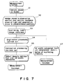
- Fig. 1 is a block diagram showing the construction bf an apparatus of automatically measuring the defect density in an object by use of a method of analyzing the object by use of scattering lights in accordance with one embodiment of the present invention.
- reference numeral 1 represents a sample (object to be observed) whose defect distribution is to be measured; 2 is a laser generator for generating a laser beam to be radiated to the sample 1; 3 is a microscope equipped with an auto-focus mechanism; 4 is a television camera for converting received scattering lights to electrical signals; and 5 is an image processor for receiving the electrical signals from the television camera and making image-processing.
- This image processor 5 has a function of processing binary image data.
- Reference numeral 6 represents a CRT (Cathode-Ray Tube) for outputting the image data as they are or defect density values, etc., obtained as a result of various calculations; 7 is a computer for controlling the system as a whole when measurement is made; 8 is a pulse motor controller; 9 is an X - Y - Z pulse stage which is driven in X-, Y-, Z-directions in accordance with the instruction of the pulse motor controller 8; and 10 is a precise sample position detector for detecting precisely the position of the sample 1.
- CTR Cathode-Ray Tube
- the defect density distribution and DZ (Denuded Zone) width of a Si wafer are usually measured. They are measured with the apparatus shown in Fig. 1 by carrying out image-processing of scattering images obtained by said light scattering method.
- Reference numeral 11 in Fig. 2 represents schematically scattering light images which are obtained by placing a half-cleaved Si wafer as the sample 1 on the pulse stage 9 in the apparatus shown in Fig. 1, radiating a laser beam to the Si wafer and observing- scattering light images through the microscope 3 from the cleavage plane side of the Si wafer.
- Reference numerals 101 and 102 represent the crystal surfaces of the Si wafer, and reference numerals 103 and 104 represent small defects having various sizes inside the Si wafer.
- the distribution of the defects (precipitates) along the depth from the surface of the crystal, which distribution is represented by reference numeral 12 in Fig. 2, can be known on the basis of such scattering light images.
- Reference numeral 105 represents a width, or so-called "DZ width", from the crystal surface 101 to a depth at which the defect density exceeds a predetermined value.
- the measurement of this DZ width is carried out by any one of the following two methods: (1) a method for measuring the DZ width on the basis of the distribution of scattering intensity in the direction of depth from the crystal surface (the distribution being one-dimensional distribution), and (2) a method of measuring the defect density in a unit volume along the depth from the crystal surface by conducting image processing on the basis of the scattering light image data.
- the accurate position of the surface of the Si wafer (sample 1) must be known. Therefore, the position of the wafer surface is adjusted or monitored by use of the precise sample position detector 10 shown in Fig. 1. This is carried out by allowing the computer 7 to input position data from the precise sample position detector 10 and driving the X - Y - Z pulse stage 9 by the pulse motor controller 8 on the basis bf this input. Next, the position of the sample stage 9 in the Z direction (perpendicular to the sheet of drawing) is adjusted by the auto-focus mechanism of the microscope 3 in order to always keep constant the position relation from the cleavage plane (the observation plane by the microscope 3) to the position at which the laser beam is incident. The sample 1 is then moved for scanning to obtain scattering light images.
- Fig. 3(a) shows scattering light images thus obtained, and is a photograph showing the crystal structure of the Si wafer.
- the intensity distribution in the direction of depth of the crystal is obtained from scattering light images as shown in Fig. 3(b).
- This Fig. 3(b) is a diagram representing the intensity distribution on line L - L' of the scattering light images obtained in Fig. 3(a).
- the DZ width 105 is defined as the distance from the surface of the crystal to the position at which the scattering intensity is a predetermined value.
- the predetermined value is set to be 30% of the average scattering intensity inside the crystal, but, in place of this value, an appropriate other value can be set separately. Since the scattering intensity distribution changes greatly from position to position at which measurement is made, the DZ width is measured at several positions and the values obtained are averaged to obtain a suitable DZ width.
- the scattering intensity of each pixel of the image data is digitized by a predetermined threshold value to obtain binary image data such as shown in Fig. 4(b).
- the data are then subjected to contraction processing (refer, for example, to Hideyuki Tamura, "Introduction To Computer Image Processing", Soken Shuppan, p. 80) in order to separate one by one the precipitates (defects) as shown in Fig. 4(c).
- the predetermined threshold value is such that it can remove noise of the television camera 4 and the defect density to be measured will be the maximum one.
- a window for counting the defect density having a sufficiently smaller width than the DZ width is set in the binary image data subjected to the contraction processing.
- the number of defects is counted while moving this window so as to obtain the distribution diagrams (see the diagram 12 in Fig. 2) of the defect density from the front surface to the back of the wafer.
- the DZ width is defined as the depth from the crystal surface to the position at which the defect density reaches a predetermined value. In this embodiment, this predetermined value is set such that the defect density is 30% of the average defect density inside the crystal, but an appropriate other value can be set separately, besides the predetermined value described above.
- Fig. 5 is a diagram showing a defect density distribution obtained by the scattering light images.
- the kinds are judged by changing the threshold value described above or effecting pattern recognition of the scattering bodies (refer to the aforementioned reference "Introduction To Computer Image Processing", page 85) in order to measure the density distribution and DZ width of each of the kinds of scattering bodies as shown in Fig. 2.
- Fig. 6 is a schematic view showing how the tomogram images (scattering light images) are obtained.
- the sample 1 to be measured is placed on the X - Y - Z pulse stage 9 in the step S1.
- the sample 1 is then moved to the observation position in the step S2, and the place of incidence of the laser beam as well as the observation plane by the microscope 3 is adjusted to each of predetermined positions.
- the pulse stage 9 is driven in the step S3 to move the sample 1 for scanning and to obtain scattering light images.
- the flow proceeds to the step S7, and if there is employed a method of obtaining the defect density distribution by image processing on the basis of the scattering light image data, the flow proceeds to the step S4.
- the digitization processing described above is made for the image data by the scattering lights in the step S4, and contraction processing is further carried out in the step S5.
- the defect density distribution and the DZ width are obtained in the step S6.
- the DZ width is found from the one-dimensional distribution of the scattering intensity in the step S7.
- Fig. 8 shows the essential components of an alternative apparatus for automatically measuring the defect density distribution according to the invention.
- the laser beam 31 is radiated into the sample 32 as the object to be observed, and the scattering lights from the defects are received by a one-dimensional photoelectric detector such as a line sensor 34 or two-dimensional photoelectric detector through an object lens 33.
- the sample 32 is moved for scanning in the direction represented by arrow to obtain an electrical output at each position of the line sensor 34. If any defects pass through the laser beam flux, the scattering lights from the defects are incident into the line sensor 34 to generate pluses. Therefore, the electrical output at each position is stored in a date buffer 35 and the pulse at each point is counted by a pulse counter 36. In this manner, the distribution of the defect density of the sample 32 can be determined.
- the objects to be observed may be single-crystal oxides, single-crystal semiconductors, glass such as optical fibers and other material through which the laser beam can pass.
- the scattering intensity (I) is expressed by the following formula.
- the scattering intensity (I) the number of the defects (n)
- Fig. 9 is a diagram showing the scattering intensity per defect particle as a function of distance (or depth) from the surface of a crystal.
- the scattering intensity per defect particle (i) is proportioned to the square of the volume of the defect particle.
- the scattering intensity per defect particle (i) is
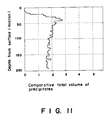
- the total volume of precipitates is expressed by the following formula:
- the total volume of precipitates (V) The volume of unit defect particle (v)
- Fig. 11 is a diagram showing the total volume of precipitates as a function of depth from the surface of the crystal.
- the present invention renders it possible to make image-processing of the images formed due to the scattering lights and determine the defect distribution in the object to be observed. Therefore, the invention enables the defects in the object to be observed three-dimensionally without the destruction of the object. Furthermore, the present invention neither require toxic liquids nor produce toxic gases unlike the etching method and is therefore highly safe. Since the present invention makes it possible to measure the defects of an object without the destruction thereof, the change of the defects which may be caused by repeatedly annealing the object can be observed and measured.
- Measurement of very small defects inside the Si crystal is very important from the viewpoint of device process, and the present invention which is highly safe, non-destructive and highly reliable is extremely effective for such measurement.
- pre-treatment such as etching of the object to be observed is not necessary and a conventional visually measuring time for which several minutes of time has been necessary per unit area observation by eyes can now be reduced to several seconds according to the present invention.
Landscapes
- Engineering & Computer Science (AREA)
- Physics & Mathematics (AREA)
- General Physics & Mathematics (AREA)
- Chemical & Material Sciences (AREA)
- Biochemistry (AREA)
- Theoretical Computer Science (AREA)
- Health & Medical Sciences (AREA)
- Life Sciences & Earth Sciences (AREA)
- Quality & Reliability (AREA)
- Analytical Chemistry (AREA)
- Computer Vision & Pattern Recognition (AREA)
- General Health & Medical Sciences (AREA)
- Immunology (AREA)
- Pathology (AREA)
- Testing Or Measuring Of Semiconductors Or The Like (AREA)
- Investigating Materials By The Use Of Optical Means Adapted For Particular Applications (AREA)
- Investigating Or Analysing Materials By Optical Means (AREA)
Claims (5)
- Méthode de détermination automatique de la densité des défauts et de la distribution des défauts dans une tranche de semiconducteur ayant une surface plane, par tomographie à dispersion laser, la méthode comprenant :l'introduction d'un faisceau laser de section réduite dans la tranche (1) à travers la surface plane, suivant une direction perpendiculaire à ladite surface, et le balayage du faisceau laser le long d'une section transversale qu'on veut inspecter ;la formation d'images par focalisation de la lumière dispersée du faisceau laser pendant le balayage ;la conversion photoélectrique des images formées en signaux électriques de diverses intensités ; etla conversion des signaux électriques en données numériques et le stockage de ces données dans une mémoire d'un ordinateur, pour constituer les données d'image de la section transversale ;
caractérisée en ce qu'elle comprend en outre :la conversion des données d'image en données d'image binaires par utilisation d'une valeur de seuil pour obtenir des images des défauts à compter ;la soumission des données d'image binaires à un traitement de contraction pour séparer les images de défaut, une par une ;l'affectation aux données d'image contractées d'une pluralité de régions dans la direction perpendiculaire à la surface plane, qui diffèrent les unes des autres en distance par rapport à la surface plane ;la détermination de la densité de défauts de chaque région par comptage du nombre des images contractées des défauts contenus dans la région ; etla détermination d'une profondeur, par rapport à la surface plane, à l'intérieur de laquelle les densités de défauts obtenues sont inférieures à une valeur prédéterminée, et la considération de la profondeur comme étant la largeur de la Zone Dénudée (ZD),c'est-à-dire de la couche exempte de défaut de la tranche. - Méthode de détermination automatique de la distribution des défauts dans une tranche de semiconducteur ayant une surface plane, par tomographie à dispersion laser, la méthode comprenant :l'introduction d'un faisceau laser à section réduite dans la tranche (1) à travers la surface plane, suivant une direction perpendiculaire à ladite surface, et le balayage du faisceau laser le long d'une section transversale qu'on veut inspecter ;la formation d'images par focalisation de la lumière dispersée du faisceau laser pendant le balayage ;la conversion photoélectrique des images formées en signaux électriques de diverses intensités ; etla conversion des signaux électriques en données numériques et le stockage de ces données dans une mémoire d'un ordinateur, pour constituer les données d'image de la section transversale ;
caractérisée en ce qu'elle comprend en outre :l'obtention d'une distribution d'intensité des données d'image sur une ligne perpendiculaire à la surface plane, comme intensités variant à intervalles d'une distance prédéterminée le long de la ligne ;la détermination d'une profondeur, par rapport à la surface plane, à l'intérieur de laquelle les intensités de la distribution d'intensité sont inférieures à une valeur prédéterminée et la considération de la profondeur comme étant la largeur de la Zone Dénudée (ZD), c'est-à-dire de la couche exempte de défaut de la tranche. - Appareil de tomographie à dispersion laser pour déterminer automatiquement la densité des défauts et la distribution des défauts dans une tranche de semiconducteur ayant une surface plane, comprenant :un dispositif (2) de génération d'un faisceau laser à section réduite ;un dispositif de positionnement (9) pour faire varier la position de la tranche de semiconducteur par rapport au faisceau laser ;un dispositif de commande (7,8) pour commander le dispositif de positionnement d'une manière telle que le faisceau laser (31) est introduit dans la tranche à travers la surface plane et que le faisceau laser est balayé le long d'une section transversale désirée de la tranche à inspecter ;un dispositif optique (3) pour former des images par focalisation de la lumière dispersée du faisceau laser pendant le balayage du faisceau laser ;un dispositif de conversion photoélectrique (4) pour convertir les images formées par le dispositif optique en signaux électriques de diverses intensités ;un dispositif de conversion analogique/numérique (5) pour convertir les signaux électriques en données numériques ; etun ordinateur (7) pour stocker les données numériques dans sa mémoire, comme données d'image de la section transversale ;
caractérisé en ce qu'il comprend en outre :un dispositif de détection (10) pour détecter la position de la surface plane dans la direction perpendiculaire à cette dernière, la position détectée étant utilisée par le dispositif de commande (7,8) pour commander exactement la position de la tranche de semiconducteur dans la direction perpendiculaire à la surface plane ; etun dispositif de traitement d'image (5) qui exécute les étapes suivantes :conversion des données d'image stockées dans la mémoire en données d'image binaires par utilisation d'une valeur de seuil pour obtenir des images de défauts à compter ;soumission des données d'image binaires à un traitement de contraction pour séparer les images de défaut une par une ;affectation aux données d'image contractées d'une pluralité de régions dans la direction perpendiculaire à la surface plane qui diffèrent les unes des autres en distance par rapport à la surface plane ;détermination de la densité de défauts de chaque région par comptage du nombre des images contractées des défauts contenus dans la région ; etdétermination d'une profondeur, par rapport à la surface plane, à l'intérieur de laquelle les densités de défauts obtenues sont inférieures à une valeur prédéterminée. - Méthode d'obtention automatique de la distribution des dimensions de défauts dans une tranche de semiconducteur ayant une surface plane, caractérisée en ce qu'elle comprend :l'introduction d'un faisceau laser à section réduite dans la tranche de semiconducteur (1) à travers la surface plane, le long d'une direction perpendiculaire à ladite surface, et le balayage du faisceau laser le long d'une section transversale qu'on désire inspecter ;la formation d'images par focalisation de la lumière dispersée du faisceau laser pendant le balayage ;la conversion photoélectrique des images formées en signaux électriques de diverses intensités ;la conversion des signaux électriques en données numériques et stockage de celles-ci dans une mémoire d'un ordinateur, comme données d'image de la section transversale;la conversion des données d'image stockées dans la mémoire en données d'image binaires par utilisation d'une valeur de seuil pour obtenir des images des défauts à compter ;la soumission des données d'image binaires à un traitement de contraction pour séparer les images de défaut une par une ;l'affectation aux données d'image contractées d'une pluralité de régions dans la direction perpendiculaire à la surface plane et à intervalles d'une distance prédéterminée le long de la dite direction ;la détermination de la densité de défauts de chaque région par comptage du nombre des images contractées des défauts contenus dans la région ;l'obtention d'une distribution d'intensité des données d'image stockées dans la mémoire et sur une ligne perpendiculaire à la surface plane, comme intensités variant aux dits intervalles ; etle calcul des diamètres moyens comparatifs des défauts de chaque région sur la base de la densité de défauts de la région et de l'intensité de la distribution d'intensité correspondant à cette région en profondeur par rapport à la surface plane et dans l'hypothèse que tous les défauts sont sphériques.
- Méthode d'obtention automatique de la distribution de volume des défauts dans une tranche de semiconducteur ayant une surface plane, caractérisée en ce qu'elle comprend :l'introduction d'un faisceau laser à section réduite dans la tranche de semiconducteur (1) à travers la surface plane, le long d'une direction perpendiculaire à ladite surface, et le balayage du faisceau laser le long d'une section transversale qu'on désire inspecter ;la formation d'images par focalisation de la lumière dispersée du faisceau laser pendant le balayage ;la conversion photoélectrique des images formées en signaux électriques de diverses intensités ;la conversion des signaux électriques en données numériques et le stockage de celles-ci dans une mémoire d'un ordinateur, comme données d'image de la section transversale ;la conversion des données d'image stockées dans la mémoire en données d'image binaires par utilisation d'une valeur de seuil pour obtenir des images des défauts à compter ;la soumission des données d'image binaires à un traitement de contraction pour séparer les images de défaut une par une ;l'affectation aux données d'image contractées d'une pluralité de régions dans la direction perpendiculaire à la surface plane qui diffèrent les unes des autres en distance par rapport à la surface plane ;la détermination de la densité de défauts de chaque région par comptage du nombre des images contractées des défauts contenus dans la région ;l'obtention d'une distribution d'intensité des données d'image stockées dans la mémoire et sur une ligne perpendiculaire à la surface plane, comme intensités variant auxdits intervalles ; etle calcul du volume total comparatif des défauts de chaque région sur la base de la densité de défauts de la région et de l'intensité de la distribution d'intensité correspondant à cette région en profondeur par rapport à la surface plane et dans l'hypothèse que tous les défauts sont sphériques.
Applications Claiming Priority (2)
| Application Number | Priority Date | Filing Date | Title |
|---|---|---|---|
| JP30942087A JP2604607B2 (ja) | 1987-12-09 | 1987-12-09 | 欠陥分布測定法および装置 |
| JP309420/87 | 1987-12-09 |
Publications (3)
| Publication Number | Publication Date |
|---|---|
| EP0319797A2 EP0319797A2 (fr) | 1989-06-14 |
| EP0319797A3 EP0319797A3 (en) | 1990-05-23 |
| EP0319797B1 true EP0319797B1 (fr) | 1996-01-31 |
Family
ID=17992789
Family Applications (1)
| Application Number | Title | Priority Date | Filing Date |
|---|---|---|---|
| EP19880119684 Expired - Lifetime EP0319797B1 (fr) | 1987-12-09 | 1988-11-25 | Méthode et appareil pour mesurer la densité de défauts et leur distribution |
Country Status (3)
| Country | Link |
|---|---|
| EP (1) | EP0319797B1 (fr) |
| JP (1) | JP2604607B2 (fr) |
| DE (1) | DE3854961T2 (fr) |
Cited By (9)
| Publication number | Priority date | Publication date | Assignee | Title |
|---|---|---|---|---|
| US7325771B2 (en) | 2004-09-23 | 2008-02-05 | The Boeing Company | Splice joints for composite aircraft fuselages and other structures |
| US7503368B2 (en) | 2004-11-24 | 2009-03-17 | The Boeing Company | Composite sections for aircraft fuselages and other structures, and methods and systems for manufacturing such sections |
| US7527222B2 (en) | 2004-04-06 | 2009-05-05 | The Boeing Company | Composite barrel sections for aircraft fuselages and other structures, and methods and systems for manufacturing such barrel sections |
| US7716835B2 (en) | 2004-04-06 | 2010-05-18 | The Boeing Company | Methods of manufacturing structural panels |
| US8042767B2 (en) | 2007-09-04 | 2011-10-25 | The Boeing Company | Composite fabric with rigid member structure |
| US8388795B2 (en) | 2007-05-17 | 2013-03-05 | The Boeing Company | Nanotube-enhanced interlayers for composite structures |
| US8641847B2 (en) | 2002-11-22 | 2014-02-04 | The Boeing Company | Composite lamination using array of parallel material dispensing heads |
| CN108474644A (zh) * | 2015-08-10 | 2018-08-31 | 慧咨环球有限公司 | 体积估计方法、设备和系统 |
| TWI861440B (zh) * | 2021-10-08 | 2024-11-11 | 南韓商二和鑽石工業股份有限公司 | 損傷層深度和損傷層內的缺陷濃度的測定方法及執行該方法的系統 |
Families Citing this family (36)
| Publication number | Priority date | Publication date | Assignee | Title |
|---|---|---|---|---|
| US6185324B1 (en) | 1989-07-12 | 2001-02-06 | Hitachi, Ltd. | Semiconductor failure analysis system |
| JP2941308B2 (ja) | 1989-07-12 | 1999-08-25 | 株式会社日立製作所 | 検査システムおよび電子デバイスの製造方法 |
| JPH0760136B2 (ja) * | 1990-05-01 | 1995-06-28 | 三井金属鉱業株式会社 | 内部欠陥検査方法および装置 |
| JPH0424541A (ja) * | 1990-05-21 | 1992-01-28 | Mitsui Mining & Smelting Co Ltd | 内部欠陥測定方法および装置 |
| FR2672124A1 (fr) * | 1991-01-25 | 1992-07-31 | Thomson Csf | Procede et dispositif de controle de l'etat de surface d'un element optique de transmission lumineuse. |
| JPH0599860A (ja) * | 1991-10-09 | 1993-04-23 | Nippon Steel Corp | 金属材料の表面品質および内部品質の評価装置および方法 |
| EP0558177B1 (fr) * | 1992-01-29 | 2000-04-12 | Advanced Micro Devices, Inc. | Système de microscope à émission resolvant d'énergie et procédé |
| JP2722362B2 (ja) * | 1992-03-27 | 1998-03-04 | 三井金属鉱業株式会社 | 粒子または欠陥の大きさ情報の測定方法および装置 |
| JP2975476B2 (ja) * | 1992-03-30 | 1999-11-10 | 三井金属鉱業株式会社 | 結晶内のフォトルミネッセンス計測方法及び装置 |
| JP2847462B2 (ja) * | 1993-11-30 | 1999-01-20 | 三井金属鉱業株式会社 | 半導体結晶の断面観察方法 |
| DE4413832C2 (de) * | 1994-04-20 | 2000-05-31 | Siemens Ag | Vorrichtungen zur Kontrolle von Halbleiterscheiben |
| DE4413831C2 (de) * | 1994-04-20 | 2000-05-31 | Siemens Ag | Verfahren zur Kontrolle von Halbleiterscheiben |
| ES2140309B1 (es) * | 1997-07-07 | 2000-09-16 | Corchos De Merida S A | Metodo de clasificacion de tapones de corcho. |
| JPH11243041A (ja) * | 1998-02-26 | 1999-09-07 | Mitsubishi Electric Corp | 品質管理システムおよび記録媒体 |
| US7137182B2 (en) | 2002-11-22 | 2006-11-21 | The Boeing Company | Parallel configuration composite material fabricator |
| US7236625B2 (en) | 2003-07-28 | 2007-06-26 | The Boeing Company | Systems and method for identifying foreign objects and debris (FOD) and defects during fabrication of a composite structure |
| US7289656B2 (en) | 2003-12-02 | 2007-10-30 | The Boeing Company | Systems and methods for determining inconsistency characteristics of a composite structure |
| US8934702B2 (en) | 2003-12-02 | 2015-01-13 | The Boeing Company | System and method for determining cumulative tow gap width |
| US7159822B2 (en) | 2004-04-06 | 2007-01-09 | The Boeing Company | Structural panels for use in aircraft fuselages and other structures |
| US7193696B2 (en) | 2004-04-12 | 2007-03-20 | United Technologies Corporation | Systems and methods for using light to indicate defect locations on a composite structure |
| US7330250B2 (en) * | 2004-05-18 | 2008-02-12 | Agilent Technologies, Inc. | Nondestructive evaluation of subsurface damage in optical elements |
| US7424902B2 (en) | 2004-11-24 | 2008-09-16 | The Boeing Company | In-process vision detection of flaw and FOD characteristics |
| US20060108048A1 (en) | 2004-11-24 | 2006-05-25 | The Boeing Company | In-process vision detection of flaws and fod by back field illumination |
| US7889907B2 (en) | 2005-01-12 | 2011-02-15 | The Boeing Company | Apparatus and methods for inspecting tape lamination |
| JP4313322B2 (ja) | 2005-02-03 | 2009-08-12 | 株式会社レイテックス | 欠陥粒子測定装置および欠陥粒子測定方法 |
| US7435947B2 (en) | 2005-10-31 | 2008-10-14 | The Boeing Company | Apparatus and methods for integrating encoding functions in material placement machines |
| US7372556B2 (en) | 2005-10-31 | 2008-05-13 | The Boeing Company | Apparatus and methods for inspecting a composite structure for inconsistencies |
| JP4905029B2 (ja) * | 2006-09-28 | 2012-03-28 | 住友金属鉱山株式会社 | 光散乱観察装置 |
| DE102008063130B4 (de) * | 2008-12-24 | 2010-10-14 | Sicrystal Ag | Verfahren zur Fremdphasenuntersuchung eines einkristallinen Substrats |
| DE102009017786B3 (de) * | 2009-04-20 | 2010-10-14 | Intego Gmbh | Verfahren zur Detektion von Fehlstellen in einer dünnen Waferscheibe für ein Solarelement sowie Vorrichtung zur Durchführung des Verfahrens |
| JP5738628B2 (ja) * | 2011-03-02 | 2015-06-24 | 株式会社コベルコ科研 | 内部欠陥検査装置および内部欠陥検査方法 |
| WO2013121110A1 (fr) * | 2012-02-13 | 2013-08-22 | Risto Orava | Procédé et agencement pour la détermination de défauts de structure de composés semi-conducteurs, amélioration du processus de croissance, et efficacité du matériau comme semi-conducteur |
| JP6308553B2 (ja) * | 2014-08-20 | 2018-04-11 | 日本電信電話株式会社 | 光ファイバの検査方法 |
| CN110118782A (zh) * | 2019-05-08 | 2019-08-13 | 中国科学院福建物质结构研究所 | 一种用于测量晶体内部介观缺陷散射的激光层析扫描仪 |
| CN113138195A (zh) * | 2021-04-16 | 2021-07-20 | 上海新昇半导体科技有限公司 | 晶体缺陷的监控方法及晶棒生长方法 |
| CN116148642B (zh) * | 2023-04-21 | 2023-07-04 | 上海聚跃检测技术有限公司 | 一种芯片失效分析方法及装置 |
Family Cites Families (4)
| Publication number | Priority date | Publication date | Assignee | Title |
|---|---|---|---|---|
| JPS54109488A (en) * | 1978-02-08 | 1979-08-28 | Fuji Photo Optical Co Ltd | Analyzing method and device of optically scattered image information |
| JPS56115945A (en) * | 1980-02-18 | 1981-09-11 | Hitachi Electronics Eng Co Ltd | Detecting device for defect of panel plate |
| JPS59149029A (ja) * | 1983-02-16 | 1984-08-25 | Agency Of Ind Science & Technol | 化合物半導体結晶基板の評価装置 |
| JP2545209B2 (ja) * | 1985-11-20 | 1996-10-16 | ラトック・システム・エンジニアリング 株式会社 | 結晶欠陥検査方法及びその検査装置 |
-
1987
- 1987-12-09 JP JP30942087A patent/JP2604607B2/ja not_active Expired - Lifetime
-
1988
- 1988-11-25 EP EP19880119684 patent/EP0319797B1/fr not_active Expired - Lifetime
- 1988-11-25 DE DE3854961T patent/DE3854961T2/de not_active Expired - Lifetime
Non-Patent Citations (1)
| Title |
|---|
| JOURNAL OF APPLIED PHYSICS, Vol. 62, No. 9, 1 November 1987, pages 3700-3703, New York, NY, USA; P. SUCHET et al.: "Evidence of the origin of infrared scattering in GaAs with high-resolution infrared tomography * |
Cited By (17)
| Publication number | Priority date | Publication date | Assignee | Title |
|---|---|---|---|---|
| US8641847B2 (en) | 2002-11-22 | 2014-02-04 | The Boeing Company | Composite lamination using array of parallel material dispensing heads |
| US8496206B2 (en) | 2004-04-06 | 2013-07-30 | The Boeing Company | Structural panels for use in aircraft fuselages and other structures |
| US7527222B2 (en) | 2004-04-06 | 2009-05-05 | The Boeing Company | Composite barrel sections for aircraft fuselages and other structures, and methods and systems for manufacturing such barrel sections |
| US7716835B2 (en) | 2004-04-06 | 2010-05-18 | The Boeing Company | Methods of manufacturing structural panels |
| US8157212B2 (en) | 2004-04-06 | 2012-04-17 | The Boeing Company | Composite barrel sections for aircraft fuselages and other structures, and methods and systems for manufacturing such barrel sections |
| US8182628B2 (en) | 2004-04-06 | 2012-05-22 | The Boeing Company | Composite barrel sections for aircraft fuselages and other structures, and methods for systems for manufacturing such barrel sections |
| US7325771B2 (en) | 2004-09-23 | 2008-02-05 | The Boeing Company | Splice joints for composite aircraft fuselages and other structures |
| US8061035B2 (en) | 2004-09-23 | 2011-11-22 | The Boeing Company | Splice joints for composite aircraft fuselages and other structures |
| US7503368B2 (en) | 2004-11-24 | 2009-03-17 | The Boeing Company | Composite sections for aircraft fuselages and other structures, and methods and systems for manufacturing such sections |
| US8168023B2 (en) | 2004-11-24 | 2012-05-01 | The Boeing Company | Composite sections for aircraft fuselages and other structures, and methods and systems for manufacturing such sections |
| US8657990B2 (en) | 2007-05-17 | 2014-02-25 | The Boeing Company | Nanotube-enhanced interlayers for composite structures |
| US8388795B2 (en) | 2007-05-17 | 2013-03-05 | The Boeing Company | Nanotube-enhanced interlayers for composite structures |
| US8042767B2 (en) | 2007-09-04 | 2011-10-25 | The Boeing Company | Composite fabric with rigid member structure |
| US8728263B2 (en) | 2007-09-04 | 2014-05-20 | The Boeing Company | Composite fabric with rigid member structure |
| CN108474644A (zh) * | 2015-08-10 | 2018-08-31 | 慧咨环球有限公司 | 体积估计方法、设备和系统 |
| CN108474644B (zh) * | 2015-08-10 | 2020-09-15 | 慧咨环球有限公司 | 体积估计方法、设备和系统 |
| TWI861440B (zh) * | 2021-10-08 | 2024-11-11 | 南韓商二和鑽石工業股份有限公司 | 損傷層深度和損傷層內的缺陷濃度的測定方法及執行該方法的系統 |
Also Published As
| Publication number | Publication date |
|---|---|
| JPH01151243A (ja) | 1989-06-14 |
| DE3854961D1 (de) | 1996-03-14 |
| EP0319797A2 (fr) | 1989-06-14 |
| EP0319797A3 (en) | 1990-05-23 |
| DE3854961T2 (de) | 1996-05-30 |
| JP2604607B2 (ja) | 1997-04-30 |
Similar Documents
| Publication | Publication Date | Title |
|---|---|---|
| EP0319797B1 (fr) | Méthode et appareil pour mesurer la densité de défauts et leur distribution | |
| EP0458418B1 (fr) | Procédé et appareil pour mesurer des défauts internes | |
| US20010029436A1 (en) | Semiconductor electrical characteristics evaluation apparatus and semiconductor electrical characteristics evaluation method | |
| US6661519B2 (en) | Semiconductor impurity concentration testing apparatus and semiconductor impurity concentration testing method | |
| US6256092B1 (en) | Defect inspection apparatus for silicon wafer | |
| US7158609B2 (en) | X-ray crystal orientation measuring method and X-ray crystal orientation measuring apparatus | |
| EP1611431B1 (fr) | Procede et appareil de detection de particules de metal sur des semiconducteurs | |
| CN1620601A (zh) | 半导体中的微缺陷的检测和分类 | |
| JPS63244753A (ja) | 結晶欠陥認識処理方法 | |
| EP0441373B1 (fr) | Procédé et appareil pour la mesure de la dimension des dessins | |
| JPH07294422A (ja) | 表面近傍結晶欠陥の検出方法およびその装置 | |
| JPH0694595A (ja) | 三次元粒子検出方法及び装置 | |
| JP2001209798A (ja) | 外観検査方法及び検査装置 | |
| JPH09243569A (ja) | 半導体基板の評価装置および評価方法 | |
| JP4313322B2 (ja) | 欠陥粒子測定装置および欠陥粒子測定方法 | |
| JPH09270447A (ja) | 結晶欠陥検出装置 | |
| JPH06221838A (ja) | 表面粗さ評価方法 | |
| Nango et al. | Minimum size of oxygen precipitates in Czochralski silicon wafers detected by improved light scattering tomography | |
| JP4823125B2 (ja) | X線結晶方位測定装置及びx線結晶方位測定方法 | |
| US20050074092A1 (en) | Digital x-ray camera for quality evaluation three-dimensional topographic reconstruction of single crystals | |
| JPH02266249A (ja) | 結晶面のx線回折測定方法 | |
| JP3667904B2 (ja) | 光散乱トモグラフ装置および観察方法 | |
| US7466798B2 (en) | Digital X-ray camera for quality evaluation three-dimensional topographic reconstruction of single crystals of biological macromolecules | |
| KR100478482B1 (ko) | 웨이퍼 검사장치 | |
| JPH0348144A (ja) | 固体の熱的状態検査装置 |
Legal Events
| Date | Code | Title | Description |
|---|---|---|---|
| PUAI | Public reference made under article 153(3) epc to a published international application that has entered the european phase |
Free format text: ORIGINAL CODE: 0009012 |
|
| AK | Designated contracting states |
Kind code of ref document: A2 Designated state(s): DE FR GB |
|
| PUAL | Search report despatched |
Free format text: ORIGINAL CODE: 0009013 |
|
| AK | Designated contracting states |
Kind code of ref document: A3 Designated state(s): DE FR GB |
|
| 17P | Request for examination filed |
Effective date: 19900712 |
|
| 17Q | First examination report despatched |
Effective date: 19910826 |
|
| GRAA | (expected) grant |
Free format text: ORIGINAL CODE: 0009210 |
|
| AK | Designated contracting states |
Kind code of ref document: B1 Designated state(s): DE FR GB |
|
| REF | Corresponds to: |
Ref document number: 3854961 Country of ref document: DE Date of ref document: 19960314 |
|
| ET | Fr: translation filed | ||
| PLBE | No opposition filed within time limit |
Free format text: ORIGINAL CODE: 0009261 |
|
| STAA | Information on the status of an ep patent application or granted ep patent |
Free format text: STATUS: NO OPPOSITION FILED WITHIN TIME LIMIT |
|
| 26N | No opposition filed | ||
| REG | Reference to a national code |
Ref country code: GB Ref legal event code: IF02 |
|
| PGFP | Annual fee paid to national office [announced via postgrant information from national office to epo] |
Ref country code: GB Payment date: 20061122 Year of fee payment: 19 |
|
| REG | Reference to a national code |
Ref country code: FR Ref legal event code: TP |
|
| PGFP | Annual fee paid to national office [announced via postgrant information from national office to epo] |
Ref country code: DE Payment date: 20071122 Year of fee payment: 20 |
|
| PGFP | Annual fee paid to national office [announced via postgrant information from national office to epo] |
Ref country code: FR Payment date: 20071108 Year of fee payment: 20 |
|
| GBPC | Gb: european patent ceased through non-payment of renewal fee |
Effective date: 20071125 |
|
| REG | Reference to a national code |
Ref country code: GB Ref legal event code: 732E |
|
| PG25 | Lapsed in a contracting state [announced via postgrant information from national office to epo] |
Ref country code: GB Free format text: LAPSE BECAUSE OF NON-PAYMENT OF DUE FEES Effective date: 20071125 |