EP0319912A2 - Procédé et dispositif pour analyser des matériaux avec des rayons X - Google Patents
Procédé et dispositif pour analyser des matériaux avec des rayons X Download PDFInfo
- Publication number
- EP0319912A2 EP0319912A2 EP19880120356 EP88120356A EP0319912A2 EP 0319912 A2 EP0319912 A2 EP 0319912A2 EP 19880120356 EP19880120356 EP 19880120356 EP 88120356 A EP88120356 A EP 88120356A EP 0319912 A2 EP0319912 A2 EP 0319912A2
- Authority
- EP
- European Patent Office
- Prior art keywords
- rays
- specimen
- metal foil
- electrons
- energy
- Prior art date
- Legal status (The legal status is an assumption and is not a legal conclusion. Google has not performed a legal analysis and makes no representation as to the accuracy of the status listed.)
- Ceased
Links
Images


Classifications
-
- G—PHYSICS
- G01—MEASURING; TESTING
- G01N—INVESTIGATING OR ANALYSING MATERIALS BY DETERMINING THEIR CHEMICAL OR PHYSICAL PROPERTIES
- G01N23/00—Investigating or analysing materials by the use of wave or particle radiation, e.g. X-rays or neutrons, not covered by groups G01N3/00 – G01N17/00, G01N21/00 or G01N22/00
- G01N23/22—Investigating or analysing materials by the use of wave or particle radiation, e.g. X-rays or neutrons, not covered by groups G01N3/00 – G01N17/00, G01N21/00 or G01N22/00 by measuring secondary emission from the material
- G01N23/223—Investigating or analysing materials by the use of wave or particle radiation, e.g. X-rays or neutrons, not covered by groups G01N3/00 – G01N17/00, G01N21/00 or G01N22/00 by measuring secondary emission from the material by irradiating the sample with X-rays or gamma-rays and by measuring X-ray fluorescence
-
- H—ELECTRICITY
- H01—ELECTRIC ELEMENTS
- H01J—ELECTRIC DISCHARGE TUBES OR DISCHARGE LAMPS
- H01J35/00—X-ray tubes
- H01J35/02—Details
- H01J35/14—Arrangements for concentrating, focusing, or directing the cathode ray
- H01J35/147—Spot size control
-
- G—PHYSICS
- G01—MEASURING; TESTING
- G01N—INVESTIGATING OR ANALYSING MATERIALS BY DETERMINING THEIR CHEMICAL OR PHYSICAL PROPERTIES
- G01N23/00—Investigating or analysing materials by the use of wave or particle radiation, e.g. X-rays or neutrons, not covered by groups G01N3/00 – G01N17/00, G01N21/00 or G01N22/00
- G01N23/02—Investigating or analysing materials by the use of wave or particle radiation, e.g. X-rays or neutrons, not covered by groups G01N3/00 – G01N17/00, G01N21/00 or G01N22/00 by transmitting the radiation through the material
-
- G—PHYSICS
- G21—NUCLEAR PHYSICS; NUCLEAR ENGINEERING
- G21K—HANDLING OF PARTICLES OR IONISING RADIATION NOT OTHERWISE PROVIDED FOR; IRRADIATION DEVICES; GAMMA RAY OR X-RAY MICROSCOPES
- G21K7/00—Gamma- or X-ray microscopes
-
- H—ELECTRICITY
- H01—ELECTRIC ELEMENTS
- H01J—ELECTRIC DISCHARGE TUBES OR DISCHARGE LAMPS
- H01J35/00—X-ray tubes
-
- H—ELECTRICITY
- H01—ELECTRIC ELEMENTS
- H01J—ELECTRIC DISCHARGE TUBES OR DISCHARGE LAMPS
- H01J35/00—X-ray tubes
- H01J35/02—Details
- H01J35/14—Arrangements for concentrating, focusing, or directing the cathode ray
- H01J35/153—Spot position control
-
- H—ELECTRICITY
- H01—ELECTRIC ELEMENTS
- H01J—ELECTRIC DISCHARGE TUBES OR DISCHARGE LAMPS
- H01J37/00—Discharge tubes with provision for introducing objects or material to be exposed to the discharge, e.g. for the purpose of examination or processing thereof
- H01J37/252—Tubes for spot-analysing by electron or ion beams; Microanalysers
- H01J37/256—Tubes for spot-analysing by electron or ion beams; Microanalysers using scanning beams
-
- G—PHYSICS
- G01—MEASURING; TESTING
- G01N—INVESTIGATING OR ANALYSING MATERIALS BY DETERMINING THEIR CHEMICAL OR PHYSICAL PROPERTIES
- G01N2223/00—Investigating materials by wave or particle radiation
- G01N2223/07—Investigating materials by wave or particle radiation secondary emission
- G01N2223/076—X-ray fluorescence
-
- H—ELECTRICITY
- H01—ELECTRIC ELEMENTS
- H01J—ELECTRIC DISCHARGE TUBES OR DISCHARGE LAMPS
- H01J35/00—X-ray tubes
- H01J35/02—Details
- H01J35/04—Electrodes ; Mutual position thereof; Constructional adaptations therefor
- H01J35/08—Anodes; Anti cathodes
- H01J35/112—Non-rotating anodes
- H01J35/116—Transmissive anodes
Definitions
- This invention relates to a method of banrudizing materials using x-rays and to apparatus therefor. More particularly, the invention relates to bangating biological specimens under ambient conditions of the environment by means of an x-ray microscope (XM). In a preferred embodiment, a novel scanning x-ray microscope (SXM) is provided and utilized in the method of the invention.
- XM x-ray microscope
- SXM novel scanning x-ray microscope
- x-rays have been utilized in many different ways for the investigation of materials including biological materials.
- Microscopes have been of great importance in the investigation of both biological and other materials.
- Optical microscopes are limited in resolution by the wavelength of the photons in a beam of visible light.
- the electron microscope (EM) was developed using the discovery of the wave property of electrons. Electrons can have extremely short wavelengths which enables the EM to have very high magnification and greatly improved resolution compared with optical microscopes. Electrons are also employed in a scanning electron microscope (SEM), which operates in a different way from the EM.
- SEM scanning electron microscope
- An SEM employs a beam of electrons focused to a spot having a diameter of several nm which is scanned over the surface of a sample in a pattern generating secondary electrons which are detected and amplified for each pixel to collectively compose a picture of the surface of the sample. Compared with an optical microscope, a far better resolution and depth of field is obtained.
- investigation of materials with an EM or SEM requires examining the specimens in an evacuated environment for the passage of electrons, as well as treatment of the specimens.
- a very thin specimen must be prepared and stained with heavy metals.
- the sample for a SEM requires coating with heavy metals.
- a scanning x-ray microscope is disclosed in United States Patent No. 4, 317, 036 granted on February 23, 1982 to Chia-Gee Wang.
- This patent discloses that prior attempts to construct x-ray microscopes were based on equipping electron microscopes with x-ray detectors and that such a system can function as an x-ray microscope with scanning electron detection.
- the invention of this patent was directed towards a more simple system in which a beam of x-rays was attempted to be focused onto a small spot for scanning the beam over a specimen, without the use of vacuum.
- x-ray analyzer electron-micro probe
- This instrument is mainly used for metallurgical studies but properly prepared biological specimens may also be analyzed.
- An optical microscope is used to identify a point of interest on the specimen to be analyzed.
- An electron beam is focused on such point on the specimen and resulting x-rays are detected and processed to provide quantitative data.
- the electron beam is focused directly onto the specimen, both the beam and the specimen being under vacuum.
- the reference further discloses the production of electron beams and detectors for detection of x-rays.
- X-rays have also been used for the detection of atoms in biological specimens using monochromatic x-rays, as disclosed in United States Patent No. 4,239,966 issued on December 16, 1980 and United States Patent No. 4,382,181 issued on May 3, 1983, both issued to Chia-Gee Wang.
- a method of investigating materials by the use of x-rays which comprises focusing an accelerated beam of electrons in an evacuated space on a metal foil facing said evacuated space, said metal foil being supported on a first surface of a support substrate which is substantially transparent to x-rays and has a second surface outside evacuated space, thereby generating x-rays in said metal foil, placing a specimen of a material to be investigated adjacent to said second surface of said substrate in a position exposed to the x-rays generated in said metal foil, and selectively detecting x-rays from said specimen which are characteristic of properties of a region of said specimen.
- an apparatus for investigating materials by the use of x- rays which comprises a chamber adapted to be maintained under vacuum, said chamber having a wall which has an aperture in which is mounted a support substrate composed of a material substantially transparent to x-rays, said support substrate having a first surface facing the interior of said chamber and a second surface facing outside said chamber, said first surface of the support substrate having thereon a metal foil exposed to the interior of the chamber, means for focusing a beam of electrons within said chamber on said metal foil, means for positioning a specimen outside said chamber adjacent to said second surface of the support substrate, and at least one x-ray detector positioned to detect x-rays leaving said specimen.
- the invention of the EM in 1932 provided biomedical scientists with a very important instrument for studying cells in fine detail.
- the resulting great progress in cell biology set the stage for the most important discoveries of modern science, namely, the identification of DNA as the carrier of genetic information by Avery and associates in 1944, and the discovery of the structure of DNA and the basis of the genetic code by Watson and Crick in 1953.
- Molecular biology emerged to become a powerful new discipline, and particularly with the introduction of recombinant DNA techniques in recent years, has undergone an explosive growth.
- a biologically viable peptide or protein for example, often cannot readily be created by simply synthesizing it from its corresponding DNA sequence.
- Much information regarding cellular controls is unknown, and fine details of cellular processes, particularly of biochemical transport, can only be studied by indirect means.
- biological specimens can be viewed using an XM or SXM in an ambient environment without subjecting the specimens to large radiation dosage or evacuation.
- Dynamic processes such as biochemical transport can thus be viewed live under controlled temperature, pH, and chemical concentration.
- Increasingly smaller targets could be resolved with improvements in beam resolution.
- 1000 ⁇ 0.1 ⁇ m
- certain viruses can be resolved and their movements followed; at 100 ⁇ , certain membrane receptors may become visible and their interactions identified; at 10 ⁇ , even individual amino acids may become visible and the peptide chemistry studied live.
- the method and apparatus of the present invention can serve to examine, for example, chemical transport in a microchip at the level of submicron structure, or phase transition in a material at a submicron domain.
- materials such as biological specimens are investigated with use of x-rays.
- the specimen is able to be investigated under ambient conditions of the environment without being subjected to high radiation dosage or evacuation.
- the x-rays which are used to investigate the specimen are produced by focusing an accelerated beam of electrons in an evacuated space or chamber onto the surface of a metal foil.
- the metal foil can be a thin layer, film or coating of a metal on a substrate.
- the metal foil should be thin and may have a thickness of 10 ⁇ m or below, and preferably is thinner, having a thickness of 5 ⁇ m or below. More preferably, the foil has a thickness less than 1 ⁇ m.
- the metal of the foil may be silver, aluminum or an aluminum alloy, or any metal which similarly emits bremsstrahlung x-ray photons upon being subjected to an electron beam (e-beam). It is desirable for the foil to be con-structed so that it will conduct and dissipate heat and electrons. For this purpose, the foil can be connected to a heat sink or a conductor for removal of electrons.
- the beam of electrons typically is accelerated to an energy within the range of 1-20 keV.
- Electrons from the beam of electrons focused on the metal layer are slowed down as they enter the metal region and emit bremsstrahlung x-ray photons.
- the electrons encounter multiple scattering in the foil and produce photons from each scattering event.
- Photons created by multiple scatterings are emitted in all directions and their energy levels range from the peak e-beam energy downwards thereby greatly broadening the spatial resolution of the e-beam.
- beam broadening is an important problem for the SXM and is considered subsequently in the present description.
- the emitted x-rays substantially comprise x-rays having a wavelength equal to or below 5 ⁇ or an energy equal to or greater than 2 keV.
- the substrate which is used to support the metal foil is made of a material which is substantially transparent to x-rays and substantially non-transparent to electrons.
- a material may be made of glass or preferably a polymer. More preferably, the substrate is made of an organic polymer.
- the electron beam is focused as a point or spot on the surface of the metal foil, and the area of x-ray peak production is not much bigger than the electron beam spot.
- the resolution may range twice or more the size of the electron spot. Therefore, it is preferred that the beam of electrons should be focused to a beam diameter of less than about 1,000 ⁇ incident on the metal foil.
- the beam is focused to a beam diameter of less than about 100 ⁇ and more preferably less than about 10 ⁇ incident on the metal foil.
- a size for the probe of electrons (the spot size) of as small as 5 ⁇ may be achieved.
- the metal foil which faces the evacuated space is supported on a first surface of the support substrate which is substantially transparent to x-rays, the support substrate having a second surface which faces outside the evacuated space.
- the specimen becomes exposed to the x-rays generated in the metal foil but is outside the evacuated space and thus is not subjected to a vacuum.
- the specimen is subjected to x-rays generated in the metal foil, which are emitted in all directions. Some of the emitted x-rays pass through the substrate and also are transmitted through the specimen.
- the x-rays entering the specimen cause the generation of fluorescent x-rays from atoms in the specimen.
- X-rays from said specimen which are characteristic of properties of a region of said specimen are selectively detected.
- the selective detection can involve the selection of either fluorescent x-rays or transmission x-rays, or both.
- Transmission x-rays characteristic of properties or structure of a region of the specimen can be selectively detected in the presence of other x-rays representing noise.
- a selection of transmission x-rays characteristic of the specimen may be done in the following way.
- the produced x-ray photons, which are far more transparent to the foil than the electrons leave an aluminum (or other metal) foil and its substrate to interact with the specimen, while a significant number of electrons cannot reach the specimen because the foil and the substrate are substantially non-transparent to electrons.
- An x-ray detector positioned to receive x-rays of a certain direction and solid angle, preferably is employed to register the x-rays with and without the specimen. Without the specimen in place, the detector simply reports the "image" of an aluminum layer plus its substrate. As shown in Fig. 3, with the specimen placed in the path of the x-ray beam, the detector reports the foil image plus the specimen. The difference of the two images, from digitized substraction, becomes the designated x-ray image of the specimen alone.
- the x-rays from said specimen are selectively detected by obtaining a first signal from x-rays detected from said specimen, obtaining a second signal from x-rays detected from the metal foil and substrate in the absence of said specimen, and digitally substracting the second signal from the first signal, thereby obtaining a digitally encoded image of a region of the specimen.
- the thickness of the specimen it is preferred to limit the thickness of the specimen to 50 ⁇ m or below, and preferably to a thickness of 1-20 ⁇ m.
- Beam broadening is a problem to be considered in many instances, depending upon the use which is intended.
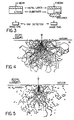
- Fig. 4 depicts a monte carlo computer simulation of the electron trajectories in an aluminum layer of one micrometer from a point source of 20 keV
- Fig. 5 shows the resultant x-ray productions, the source of these simulations being R.
- the metal foil e.g. an aluminum layer
- the metal foil preferably is coated onto an organic substrate.
- the substrate provides mechanical strength and is useful to support metal layers of different chosen thicknesses.
- the substrate must provide mechanical strength without generating intense x-rays.
- the coated aluminum layer facing the incident electron beam generates x-rays, conducts charge, and dissipates heat.
- the monte carlo calculation in Figs. 4 and 5 assumed a point electron beam to result in a broadened x-ray beam. If the incident electron beam has a finite beam size, this broadened x-ray spot must include one-half of the point broadening to all directions of the finite electron beam size, resulting in a point broadening in addition to the electron beam size.
- each scattering gives rise to bremsstrahlung radiation.
- the distribution of scattering energies is a well defined function of the electron beam energy as well as the foil thickness. If x-rays are selected from only the peak energy, the x-ray beam size would essentially be confined to the incident electron beam spot because no multiple scattering could take place to degrade the beam definition without first degrading the electron energy.
- a energy dispersive x-ray detector can easily discriminate and select only the peak energy for registration, thereby recording only those x-rays generated from the electron beam spot.
- a properly positioned axial symmetric diffractor such as a graphite crystal, also helps to channel higher energy photons from a larger solid angle to reach the detector while blocking the passage of lower energy photons.
- Another way to channel the distribution of x-rays mainly toward the peak energy is to reduce the thickness of the metal foil so that multiple scatterings in the foil are initially reduced.
- the step of detecting x-rays from the specimen it is a preferred embodiment of the present invention to detect principally only x-rays selected from those having a peak energy or an energy close to the peak energy.
- the position of the accelerated electron beam is moved so that an area of metal foil is scanned by the beam of electrons, there providing a SXM.
- the scanning movement of the electron beam is done by conventional techniques as are known in the operation of a SEM. This may be done, for example, by utilizing a modified SEM wherein the electron beam is accelerated and scanned, but the specimen is placed outside of the SEM adjacent to an aperture holding a metal foil exposed to the scanning electron beam and supported by a support substrate having a surface outside the SEM against which the specimen is located.
- signals representative of an image of a region of the specimen are obtained, by the processing of detected x-rays representative of different parts of the region obtained during the scanning process.
- a digitally encoded image of a region of the specimen is obtained and amplified, and may be displayed, such as by means of an electron beam in a cathode ray tube.
- the electron beam in said cathode ray tube is scanned in synchronization with the scanning of the beam of electrons directed to the metal foil.
- the obtained image can be element specific.
- an energy dispersive x-ray detector is used which is also energy discriminating.
- Transmission x-rays leave the specimen in a forward direction (downstream direction of the e-beam) and would represent noise or background when it is desired to selectively detect fluorescent photons.
- Fluorescent x-rays do not have a forward intensity peak.
- the fluorescent x-ray detector should be placed outside of the main e-beam path. It is a further preferred embodiment of the invention to selectively detect fluorescent x-rays emitted from the specimen.
- Fluorescent x-rays characteristic of a specific chemical element may be detected and a signal produced which is representative of the concentration of the specific chemical element in the specimen.
- the energy selectivity of the x-ray detector can be used to analyze the chemical composition of the specimen, i.e., selected to report the characteristic fluorescent x-rays.
- the electron beam energy should be controlled to be near a major absorption edge of the element in question. In other words, each element of interest in the specimen should be examined with an electron beam energy set at near the characteristic energy of the element for a good beam definition.
- This method can be used as a chemical scan of sub-micron dimension with or without the positional variation (scanning the electron beam over a region of the metal foil).
- a static spot analysis of chemical composition can be obtained without positional scanning, i.e. with the XM of the present invention, and provides important information. Repeated over a time interval, the changes in elemental or chemical composition of a region or a spot in the specimen can be determined.
- the energy of the accelerated beam of electrons is preferably maintained at substantially the same as the energy of the fluorescent x-rays characteristic of the specific chemical element.
- the energy of the accelerated beam of electrons may be sequentially changed to provide a series of different energies corresponding to different energies of fluorescent x-rays characteristic of the different chemical elements, with production of signals representing the concentration of a plurality of such chemical elements in the specimen.
- the method of the invention further includes obtaining different signals over a period of time which represent the changing concentrations of those different chemical elements in the specimen.
- a dynamic electron beam energy scan may be employed together with gate variation of the x-ray detector.
- the dynamic energy scan controls the anode voltage of an electron gun and associated electromagnetic lenses as well as the detector window. These controls are useful to maintain a good x-ray beam definition.
- Fig. 1 illustrates an embodiment of an XM, shown generally as 1, of the present invention
- Fig. 2 illustrates a SXM embodiment, shown generally as 1 a , of the present invention
- the apparatus of the invention comprises a chamber 2 which comprises a generally elongated chamber housing 2 a and at opposite ends of said housing a first end wall 2 b and a second end wall 2 c .
- the second end wall 2 c has an aperture 2 d .
- a support substrate 13 is mounted in or adjacent to aperture 2 c , the support substrate 13 being composed of a material substantially transparent to x-rays and having a first surface 13 a facing the interior of chamber 2 and a second surface 13 b facing outwardly of said chamber 2.
- a metal foil 12 is disposed on first surface 13 a of said substrate 13.
- the metal foil is a thin layer but for clarity is exaggerated in thickness in the Figs. 1 and 2.
- Metal foil 12 thus is in a position exposed to the interior of chamber 2.
- the chamber is capable of being evacuated and maintained under vacuum, for example by means of vacuum pump 8.
- the apparatus of the invention further comprises means for producing and accelerating a beam of electrons 9 within said chamber 2 along a beam path.
- the electron beam may be produced by an electron gun 3 and accelerated by anode 4, with electric current supply 5 supplying filament heating power to the electron gun 3 and high voltage power to anode 4, through electric current conductors shown in Figs. 1 and 2 by arrows.
- the beam of electrons alternatively may be generated outside of chamber 2 by other means.
- Said chamber 2 preferably is an elongated hollow body, with the means for producing and accelerating the beam of electrons 9 being adjacent to the first end wall 2 b , and the support substrate 13 being mounted in second end wall 2 c , the electron beam path extending along a lengthwise axis in a downstream direction from the means for producing and accelerating the beam of electrons to the metal foil 12.
- Means is provided for focusing the beam of electrons 9 within said chamber.
- the means for focusing may comprise electromagnetic condenser lens 6 and objective lens 7, electric current supply 10 for the condenser lens and electric current supply 11 for the objective lens, the electric current conductors being depicted by arrows.
- Means such as specimen holder 15 is provided for positioning a specimen 14 (shown exaggerated in thickness) outside said chamber 2 adjacent to the second surface 13 b of substrate 13.
- specimen holder 15 may comprise a cup for specimens dispersed in water or other liquid, or a clamp for solid phase specimens.
- X-ray detector 18 for fluorescent x-rays 17 and/or x-ray detector 22 for transmission x-rays 16 are disposed in a location where they are capable of detecting x-rays leaving said specimen 14.
- a preamplifier 19 and 23 Cooperating with each x-ray detector 18 and 22 is a preamplifier 19 and 23, respectively.
- X-ray detector selector switch 24 is provided to divert the output of one or the other preamplifier to amplification, signal processing and display units.
- X-ray detector 22 is located downstream from the means for positioning a specimen, in the path of axial x-rays 21 transmitted from specimen 14, and said means for positioning a specimen and said x-ray detector 22 are disposed in alignment with the lengthwise axis of chamber 2.
- X-ray detector 18 is positioned out of alignment with the lengthwise axis of chamber 2, and is substantially out of the path of x-rays 16 transmitted through said specimen 14, and is in the path of fluorescent x-rays 17 emitted from specimen 14.
- x-ray detector 18 for fluorescent x-rays is shown in Figs. 1 and 2 as preferably being disposed outside of chamber 2, this detector may instead be positioned inside chamber 2 or disposed outside chamber 2 adjacent to or in an aperture in chamber housing 2 a (not shown in the figures), said aperture being sealed by a window or detector window which is transparent to x-rays.
- Detector 18 can be placed in the alternative positions indicated or it can be maintained in the position shown in the drawings and an additional fluorescent x-ray detector can be placed in the alternative positions.
- the x-ray detectors are preferably energy dispersive and energy discriminating.
- X-ray detector 22 of this type is thereby capable of selecting and recording a narrow range of peak energy and energies close to peak energy, to assist in the recording of only the x-rays generated from the electron beam spot.
- An axial symmetric defractor 20 may also be included, to direct x-rays 21 having energies close to peak energy towards x-ray detector 22, while blocking the passage of lower energy x-rays.
- the defractor 20, which may comprise a graphite crystal, is disposed between the specimen holder 15 and x-ray detector 22, in axial alignment with the lengthwise axis of chamber 2.
- the apparatus of the invention may include means for amplifying a signal representative of the detected x-rays.
- the output from the preamplifier 19 or 23 is conducted by detector selector switch 24, to a pulse amplifier and a multi-channel analyzer 25.
- the signal from analyzer 25 is transmitted to A/D (analog-to-digital) converter, memory and processor 26, the output of which may be conducted for display to a video amplifier 27 which controls a display unit comprising CRT (Cathode ray tube) 28.
- the CRT display unit may be a computer monitor.
- Energy dispersive x-ray detectors usually require a multi-channel analyzer to distinguish one pulse height from another. But with the use of personal computers, the multi-channel analyzer and discriminator, together with the A/D convertor, digitized image memories and processing can all be processed by a PC-AT with a modification board. The high speed of an AT unit is needed in order to complete the data processing in a reasonable time.
- the imaged output can be handled on the AT computer by using a high-resolution extended graphics board in combination with a high-resolution color monitor which produces a color image, with each separate color representing a different element.
- the minimum resolution desirably should be 640 x 400 pixels.
- a preferred embodiment of the apparatus of the present invention is a SXM as illustrated in Fig. 2.
- the SXM apparatus as illustrated further comprises means for scanning the beam of electrons 9 over an area of the metal foil 12. This is accomplished by further modification of the Fig. 1 apparatus, as shown in Fig. 2, by the provision of a scanning coil 29 which can sweep the electron beam in a scanning pattern generated by a scanning generator 30, the output of which is directed to a scanning amplifier 31 which in turn is connected to scanning coil 29.
- the output of the scanning generator 30 also is directed to CRT display unit 28 so that the cathode ray tube is scanned in synchronization with the scanning of the metal foil.
- the architecture of a usual scanning electron microscope (SEM) was used, but in place of the SEM's focal position of the specimen, a thin foil with a metal coating is instead located.
- the said foil serves several functions unrelated to the usual SEM. It seals the vacuum of the e-beam chamber so that while one side of the foil faces the evacuated e-beam, the other side is exposed to the ambient pressure and humidity; it conducts charge from the e-beam; it dissipates heat from the beam irradiation; and it generates x-rays to illuminate the specimen positioned outside the evacuated chamber.
- An important feature of the above disclosure is that a very fine x-ray beam spot, almost as small as the e-beam spot of the SEM, is created for the x-ray microscope. As the e-beam slows down in metal, it generates x-rays and the beam spot diffuses and broadens along the way, but only the relatively un-broadened x-ray spot is utilized for the specimen image. This relatively un-broadened x-ray beam is chosen by selecting the peak x-ray photon energies originating rom the e-beam prior to its energy degradation and broadening. Another mode of operation is to use a very thin metal layer whose thickness is of the order of the designated x-ray beam spot size.
- Iodine for example, is a heavy element, which provides contrast to the normal biological specimens of light elements, and Iodine can be incorporated into various proteins and peptides without causing major alteration to the biochemical structure.
- Bromine in the form of BrdU, can be incorporated into the nucleic acids for enhancing the contrast.
- the e-beam energy can be raised, albeit at the price of a reduced contrast.
- CCD optical charged-coupled-deviced
- Another important advantage of using the small pixel CCD is its small capacitance in each pixel, therefore very low noise; of the order of the Si(Li) detector operating at the liquid nitrogen temperature while operating CCD at the room temperature.
- a series of recent developments in using the CCD's for the x-rays can be found in several articles in OPTICAL ENGINEERING, Vol. 26, No. 2,8, and 10; 1987.
- an optical CCD with very shallow depletion region can also serve for x-ray detection with the help of a fluorescent screen. X-rays shining on the fluorescent screen would be converted into optical photons and be detected by the optical CCDs.
- a fiber screen with low numerical aperature can be placed between the fluorescent screen and the detector array: In this arrangement, the detectors are no longer energy discriminating.
- the metal coating can be made very thin, as thin as the designated x-ray beam spot size.
- the e-beam can be tilted to benefit from the maximum dipole radiation from the primary e-beam prior to its diffusive scattering (see Fig. 7).
Landscapes
- Chemical & Material Sciences (AREA)
- Analytical Chemistry (AREA)
- Physics & Mathematics (AREA)
- Health & Medical Sciences (AREA)
- Life Sciences & Earth Sciences (AREA)
- Biochemistry (AREA)
- General Health & Medical Sciences (AREA)
- General Physics & Mathematics (AREA)
- Immunology (AREA)
- Pathology (AREA)
- Engineering & Computer Science (AREA)
- General Engineering & Computer Science (AREA)
- High Energy & Nuclear Physics (AREA)
- Analysing Materials By The Use Of Radiation (AREA)
Applications Claiming Priority (2)
| Application Number | Priority Date | Filing Date | Title |
|---|---|---|---|
| US12947687A | 1987-12-07 | 1987-12-07 | |
| US129476 | 1993-09-30 |
Publications (2)
| Publication Number | Publication Date |
|---|---|
| EP0319912A2 true EP0319912A2 (fr) | 1989-06-14 |
| EP0319912A3 EP0319912A3 (fr) | 1990-05-09 |
Family
ID=22440152
Family Applications (1)
| Application Number | Title | Priority Date | Filing Date |
|---|---|---|---|
| EP88120356A Ceased EP0319912A3 (fr) | 1987-12-07 | 1988-12-06 | Procédé et dispositif pour analyser des matériaux avec des rayons X |
Country Status (2)
| Country | Link |
|---|---|
| EP (1) | EP0319912A3 (fr) |
| JP (1) | JPH02138856A (fr) |
Cited By (8)
| Publication number | Priority date | Publication date | Assignee | Title |
|---|---|---|---|---|
| EP0432568A3 (en) * | 1989-12-11 | 1991-08-28 | General Electric Company | X ray tube anode and tube having same |
| WO1996029723A1 (fr) * | 1995-03-20 | 1996-09-26 | Medixtec Gmbh Medizinische Geräte | Installation radiographique a microfoyer |
| WO1998013853A1 (fr) * | 1996-09-27 | 1998-04-02 | Bede Scientific Instruments Limited | Generateur de rayons x |
| EP1679733A3 (fr) * | 2004-01-23 | 2007-04-04 | Tohken Co., Ltd. | Appareil d'inpection microscopique à rayons X |
| US9748070B1 (en) | 2014-09-17 | 2017-08-29 | Bruker Jv Israel Ltd. | X-ray tube anode |
| CN110856658A (zh) * | 2018-08-23 | 2020-03-03 | 西门子医疗有限公司 | X射线设备的患者躺卧设备和适配其患者卧床的方法 |
| US11302508B2 (en) | 2018-11-08 | 2022-04-12 | Bruker Technologies Ltd. | X-ray tube |
| EP4143870A4 (fr) * | 2021-05-05 | 2024-05-15 | Rad Source Technologies, Inc. | Système à transmission directe de rayons x par manipulation d'électrons et procédés d'utilisation |
Families Citing this family (7)
| Publication number | Priority date | Publication date | Assignee | Title |
|---|---|---|---|---|
| JP3191554B2 (ja) * | 1994-03-18 | 2001-07-23 | 株式会社日立製作所 | X線撮像装置 |
| JP3569152B2 (ja) | 1998-10-15 | 2004-09-22 | 株式会社マキタ | バッテリーパック |
| JP4921629B2 (ja) * | 2000-03-31 | 2012-04-25 | パナソニック株式会社 | 流体冷却式電池パックシステム |
| JP2001307669A (ja) * | 2000-04-21 | 2001-11-02 | Shimadzu Corp | 軟x線発生装置及びx線検査装置 |
| JP4608820B2 (ja) * | 2001-06-26 | 2011-01-12 | 株式会社島津製作所 | X線検査装置 |
| JP5626757B2 (ja) | 2010-02-24 | 2014-11-19 | 独立行政法人産業技術総合研究所 | X線顕微鏡像観察用試料支持部材、x線顕微鏡像観察用試料収容セル、およびx線顕微鏡 |
| JP5750763B2 (ja) | 2011-09-09 | 2015-07-22 | 国立研究開発法人産業技術総合研究所 | X線顕微鏡用試料収容セルおよびx線顕微鏡像の観察方法 |
Family Cites Families (2)
| Publication number | Priority date | Publication date | Assignee | Title |
|---|---|---|---|---|
| US4519092A (en) * | 1982-10-27 | 1985-05-21 | Albert Richard D | Scanning x-ray spectrometry method and apparatus |
| JPS6244940A (ja) * | 1985-08-22 | 1987-02-26 | Shimadzu Corp | X線源 |
-
1988
- 1988-12-06 EP EP88120356A patent/EP0319912A3/fr not_active Ceased
- 1988-12-07 JP JP63307967A patent/JPH02138856A/ja active Pending
Cited By (11)
| Publication number | Priority date | Publication date | Assignee | Title |
|---|---|---|---|---|
| EP0432568A3 (en) * | 1989-12-11 | 1991-08-28 | General Electric Company | X ray tube anode and tube having same |
| WO1996029723A1 (fr) * | 1995-03-20 | 1996-09-26 | Medixtec Gmbh Medizinische Geräte | Installation radiographique a microfoyer |
| US5857008A (en) * | 1995-03-20 | 1999-01-05 | Reinhold; Alfred | Microfocus X-ray device |
| WO1998013853A1 (fr) * | 1996-09-27 | 1998-04-02 | Bede Scientific Instruments Limited | Generateur de rayons x |
| US6282263B1 (en) | 1996-09-27 | 2001-08-28 | Bede Scientific Instruments Limited | X-ray generator |
| EP1679733A3 (fr) * | 2004-01-23 | 2007-04-04 | Tohken Co., Ltd. | Appareil d'inpection microscopique à rayons X |
| US9748070B1 (en) | 2014-09-17 | 2017-08-29 | Bruker Jv Israel Ltd. | X-ray tube anode |
| CN110856658A (zh) * | 2018-08-23 | 2020-03-03 | 西门子医疗有限公司 | X射线设备的患者躺卧设备和适配其患者卧床的方法 |
| CN110856658B (zh) * | 2018-08-23 | 2023-07-14 | 西门子医疗有限公司 | X射线设备的患者躺卧设备和适配其患者卧床的方法 |
| US11302508B2 (en) | 2018-11-08 | 2022-04-12 | Bruker Technologies Ltd. | X-ray tube |
| EP4143870A4 (fr) * | 2021-05-05 | 2024-05-15 | Rad Source Technologies, Inc. | Système à transmission directe de rayons x par manipulation d'électrons et procédés d'utilisation |
Also Published As
| Publication number | Publication date |
|---|---|
| EP0319912A3 (fr) | 1990-05-09 |
| JPH02138856A (ja) | 1990-05-28 |
Similar Documents
| Publication | Publication Date | Title |
|---|---|---|
| US5044001A (en) | Method and apparatus for investigating materials with X-rays | |
| Duncumb | Enhanced X-ray emission from extinction contours in a single-crystal gold film | |
| EP0319912A2 (fr) | Procédé et dispositif pour analyser des matériaux avec des rayons X | |
| JP3752252B2 (ja) | 電気的に絶縁された標本表面の分析装置 | |
| US6548810B2 (en) | Scanning confocal electron microscope | |
| JP3191554B2 (ja) | X線撮像装置 | |
| EP0444085B1 (fr) | Detecteur d'electrons ameliore destine a etre utilise dans un environnement gazeux | |
| US20150055745A1 (en) | Phase Contrast Imaging Using Patterned Illumination/Detector and Phase Mask | |
| US20040208280A1 (en) | X-ray microscopic inspection apparatus | |
| JP7105647B2 (ja) | 透過型荷電粒子顕微鏡における回折パターン検出 | |
| US10832901B2 (en) | EELS detection technique in an electron microscope | |
| JP2019145499A (ja) | 走査透過荷電粒子顕微鏡におけるインテリジェントプレスキャン | |
| JPH0727556Y2 (ja) | 荷電粒子エネルギ分析装置 | |
| US4724320A (en) | Method of observing the arrangement of atoms on a surface and apparatus therefor | |
| JP4565168B2 (ja) | 走査型x線顕微鏡および走査型x線顕微鏡像の観察方法 | |
| EP1155419B1 (fr) | "microscopes aux rayons x comprenant une source de rayons x pour rayons x mous | |
| Lovric et al. | In situ correlative helium ion microscopy and secondary ion mass spectrometry for high-resolution nano-analytics in life sciences | |
| Kumar | Microscopy, working and types | |
| Kammlott | Some aspects of scanning electron microscopy | |
| JP2000292380A (ja) | 陽電子消滅分析装置 | |
| JP3663439B2 (ja) | X線撮像装置および方法 | |
| JPH1167138A (ja) | 微小領域観察装置 | |
| CN117438268A (zh) | 使用带电粒子显微镜检查样品的方法 | |
| Shchelokov et al. | Scanning X-ray microscope | |
| Tanno | Fine imaging scanning electron microscope due to secondary electron multiplication and optical configuration |
Legal Events
| Date | Code | Title | Description |
|---|---|---|---|
| PUAI | Public reference made under article 153(3) epc to a published international application that has entered the european phase |
Free format text: ORIGINAL CODE: 0009012 |
|
| AK | Designated contracting states |
Kind code of ref document: A2 Designated state(s): AT BE CH DE ES FR GB GR IT LI LU NL SE |
|
| PUAL | Search report despatched |
Free format text: ORIGINAL CODE: 0009013 |
|
| AK | Designated contracting states |
Kind code of ref document: A3 Designated state(s): AT BE CH DE ES FR GB GR IT LI LU NL SE |
|
| 17P | Request for examination filed |
Effective date: 19901102 |
|
| 17Q | First examination report despatched |
Effective date: 19920206 |
|
| RIN1 | Information on inventor provided before grant (corrected) |
Inventor name: WANG, CHIA-GEE, DR. |
|
| RAP1 | Party data changed (applicant data changed or rights of an application transferred) |
Owner name: NANODYNAMICS, INCORPORATED |
|
| STAA | Information on the status of an ep patent application or granted ep patent |
Free format text: STATUS: THE APPLICATION HAS BEEN REFUSED |
|
| 18R | Application refused |
Effective date: 19950323 |