EP0319973B1 - Spreizspektrum-Demodulationseinrichtung für ein Spreizspektrum-Übertragungssystem - Google Patents
Spreizspektrum-Demodulationseinrichtung für ein Spreizspektrum-Übertragungssystem Download PDFInfo
- Publication number
- EP0319973B1 EP0319973B1 EP88120525A EP88120525A EP0319973B1 EP 0319973 B1 EP0319973 B1 EP 0319973B1 EP 88120525 A EP88120525 A EP 88120525A EP 88120525 A EP88120525 A EP 88120525A EP 0319973 B1 EP0319973 B1 EP 0319973B1
- Authority
- EP
- European Patent Office
- Prior art keywords
- signal
- spread spectrum
- output
- demodulating device
- spread
- Prior art date
- Legal status (The legal status is an assumption and is not a legal conclusion. Google has not performed a legal analysis and makes no representation as to the accuracy of the status listed.)
- Expired - Lifetime
Links
Images
Classifications
-
- H—ELECTRICITY
- H04—ELECTRIC COMMUNICATION TECHNIQUE
- H04B—TRANSMISSION
- H04B1/00—Details of transmission systems, not covered by a single one of groups H04B3/00 - H04B13/00; Details of transmission systems not characterised by the medium used for transmission
- H04B1/69—Spread spectrum techniques
- H04B1/707—Spread spectrum techniques using direct sequence modulation
- H04B1/7073—Synchronisation aspects
- H04B1/7075—Synchronisation aspects with code phase acquisition
Definitions
- the present invention relates to a spread spectrum communication system and, more particularly, to a spread spectrum demodulating device for demodulating a spread spectrum signal by inverse spread.
- a spread spectrum signal is produced by spreading to N-fold a PSK (Phase Shift Keying) modulated data signal or PSK modulated signal by a PN (Pseudo Noise) signal.
- a device for receiving and demodulating the spread spectrum signal is generally constituted by a spread spectrum demodulating device and a PSK demodulating device.
- the spread spectrum demodulating device demodulates the PSK modulated signal by inversely spreading the received spread spectrum signal, while the PSK demodulating device regenerates the data signal by applying synchronization detection to the demodulated PSK modulated signal.
- a prior art spread spectrum demodulating device which precedes a PSK demodulating device includes a mixer for inversely spreading an input spread spectrum signal to produce a demodulated PSK modulated signal.
- the demodulated PSK modulated signal is passed through a band-pass filter to obtain a predetermined processing gain and then applied to a detector for envelop detection.
- the resulting output of the detector is fed to a comparator to determine whether or not a demodulated PSK modulated signal has been detected.
- This kind of device has a drawback that the decision associated with a demodulated PSK modulated signal comes to involve errors and eventually results in malfunctions as the carrier-to-noise (C/N) ratio after the propagation of the signal through the band-pass filter approaches zero decibel.
- C/N carrier-to-noise
- each detector has a low-pass filter at its output stage and makes the band width of the filter extremely narrow under low C/N conditions so as to suppress the signal diffusion. This not only slows down the response but also results in a prohibitively long capture time.
- the prior art device is extremely complicated in construction.
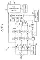
- the prior art spread spectrum demodulating device 10 is located at a stage which precedes a PSK demodulating device 12 and a controller 14 thereof.
- the demodulating device 10 is made up of a splitter 16, mixers 18a, 18b and 18c, band-pass filters (BPFs) 20a, 20b and 20c, detectors 22a, 22b and 22c, comparators 24a, 24b and 24c, a synchronization detector 26, a sweep controller 28, a subtractor 30, a loop filter 32, a voltage-controlled oscillator (VCO) 34, an AND gate 36, and a PN generator 38.
- BPFs band-pass filters
- VCO voltage-controlled oscillator
- a spread spectrum signal is split into three by the splitter 16 to be applied to one input of the three mixers 18a to 18c.
- the spread spectrum signal 40 is produced by spreading a PSK modulated data signal spectrum to N-fold (N being an integer) by use of a PN signal.
- the PN generator 38 generates PN signals 42a, 42b and 42c in response to an output of the AND gate 36 (spread clock) and delivers them to the other input of the mixers 18a, 18b and 18c.
- the three PN signals 42a to 42c are generated in such a relation that the PN signal 42a has the same phase as the input spread clock, the PN signal 42b is advanced in phase by half the clock relative to the input spread clock, and the PN signal 42c is delayed by half the clock relative to the same.
- Applied to one input of the AND gate 36 is an output of the VCO 34 (i. e. spread clock) and to the other input is an output of the sweep controller 28 (i. e. sweep control signal).
- the VCO 34 generates a spread clock having a predetermined frequency by using an output of the loop filter 32 as a control voltage.
- the sweep controller 28 When the output of the synchronization detector 26 is indicative of "synchronized,” the sweep controller 28 holds the sweep control signal at a (logical) ONE level so that the output of the VCO 34 may appear on the output of the AND gate 36 as it is. Conversely, when the output of the synchronization detector 26 is indicative of "non-synchronized,” the sweep controller 28 turns the level of the sweep signal to a (logical) ZERO level for the duration of one clock pulse every predetermined period of time, thereby causing one clock pulse to be lost at every predetermined interval.
- the mixers 18a to 18c inversely spread the input spread spectrum signal by their associated PN signals 42a to 42c so as to demodulate the PSK modulated signal.
- Outputs of the mixers 18a to 18c are individually applied to the BPFs 20a to 20c to be thereby provided with a predetermined processing gain.
- the outputs of the BPFs 20a to 20c are individually fed to the detectors 22a and 22c for envelope detection and therefrom to the comparators 24a to 24c.
- the outputs of the detectors 22b and 22c are delivered to the subtractor 30.
- the resulting output of the subtractor 30 is routed through the loop filter 32 to the VCO 34 to serve as a control voltage.
- the comparators 24a to 24c each compares the level of the input signal with a threshold level and delivers the result to the synchronization detector 26. When none of the comparators 24a to 24c is indicative of detection of a PSK modulated signal, the synchronization detector 26 turns its output to the sweep controller 28 into "non-synchronized”. On the other hand, when any of the comparators 24a to 24c is indicative of detection of a PSK modulated signal, the synchronization detector 26 turns its output into "synchronized”. Upon the change of the output of the synchronization detector 26 to "synchronized,” an output of the VCO 34 is directly applied to the PN generator 38 in the form of a spread clock to thereby establish a delay-lock loop.
- the PSK modulated signal demodulated by the delay-lock loop appears on the output of the mixer 18a and is applied to the PSK demodulating device 12, whereby demodulated data 44 and a demodulated clock 46 are obtained.
- the controller 14 is adapted to control the PSK demodulating device 12.
- a problem with the prior art demodulating device 10 is as follows. As the carrier-to-noise (C/N) ratio after the PSK modulated signal demodulated by the inverse spread of the spread spectrum signal has been provided with a predetermined processing gain by band-pass filtering sequentially approaches zero decibel, the signal decision performed by the individual comparators 24a to 24c comes to involve errors and eventually results in malfunctions. Further, since the detectors 22a to 22c each has a low-pass filter at its output stage and makes the band width of the filter extremely narrow under low C/N ratio conditions so as to suppress signal spread, not only the response is slow but also a prohibitively long period of time expires before the capture. In addition, the delay-lock loop which constitutes the major part of the demodulating device 10 renders the whole arrangement extremely complicated.
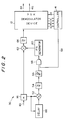
- a spread spectrum demodulating device embodying the present invention is shown and generally designated by the reference numeral 50.
- the demodulating device 50 comprises a splitter 16, a first mixer 52, a first BPF 54, a phase shifter 56, an AND gate 58, a PN generator 60, a second mixer 62, a second BPF 64, and a 1/2 bit delay circuit 66.
- the splitter 16 feeds an incoming spread spectrum signal 40 to one input of the first mixer 52 and the delay circuit 66 as well as to one input of the second mixer 62.
- the delay circuit 66 delays the input signal 40 by each half bit and feeds its output to the other input of the first mixer 52.
- a signal produced by converting the spread spectrum signal of an intermediate frequency band into the baseband appears on the output of the first mixer 52.
- a spread clock component appears in the output of the first mixer 52, a recovered version of the spread clock is separated by the first BPF 54.
- the recovered spread clock is applied to one input of the AND gate 58 after being adjusted in phase by the phase shifter 56.
- Applied to the other input of the AND gate 58 is a 1-bit sweep control signal 68 from the controller 14.
- the recovered spread clock undergone phase adjustment as mentioned is fed from the AND gate 58 to the PN generator 60 in response to the sweep control signal 68.
- the sweep control signal 68 plays the same role as the prior art sweep control signal.
- the PN generator 60 therefore generates a PN signal in response to the recovered spread clock and delivers it to the other input of the second mixer 62. Since the recovered spread clock is directly obtained from the received spread spectrum signal 40, it will be seen that the bit pattern of the PN signal generated by the PN generator 60 is synchronous to the bit pattern of the spread spectrum signal 40 while being deviated from the latter by any desired number of bits.
- the second mixer 62 inversely spreads the spread spectrum signal 40 by using the PN signal. An output of the mixer 62 is applied to the second BPF 64 for removing unnecessary waves and then to the PSK demodulating device 12.
- the mixer 62 is capable of correctly demodulating the PSK modulated signal only if the spread spectrum signal 40 and the PN signal are coincident with respect to the bit pattern.
- the controller 14 for monitoring the operations of the PSK demodulating device 12 is supplied with input frequency deviation detection signals a and b , a synchronization or sync decision signal c and a sweep stop and cancel signal d from the PSK demodulating device 12 while supplying a frequency sweep signal (for AFC) e to the demodulating device 12.
- the controller 14 When the demodulating operation of the demodulating device 12 is not correct, the controller 14 generates a sweep control signal 68 which causes the regenerated spread clock coming out of the AND gate 58 to be lost by one pulse at every predetermined interval. If the demodulating operation is correct, the sweep control signal 68 from the controller 14 is such that it allows an output of the phase shifter 56 to be directly applied to the PN generator 60.
- This kind of monitoring function assigned to the controller 14 is a traditional basic function, and the sweep control signal 68 can be led out without resorting to any special implementation.
- An example of the controller 14 is disclosed in JP-A-63 178 642.
- the controller 14 detects it by referencing the operations of the PSK demodulating device 12 and then generates the sweep control signal 68.
- an intermittently omitted recovered spread clock is applied to the PN generator 60 to cause the latter to generate a 1-bit shifted PN signal.
- Such a shift is repeated a plurality of times until the two patterns coincide with each other.
- This allows the second mixer 62 to perform inverse spread correctly and thereby allows a correctly demodulated PSK modulated signal to be fed to the PSK demodulating device 12.
- a data signal is regenerated with accuracy to form the demodulated data 44 and clock 46.
- the controller 14 changes the status or content of the sweep control signal 68.
- the present invention provides a spread spectrum demodulating device which eliminates the need for a traditional delay-lock loop, i.e., it allows a spread clock to be directly recovered from a received spread spectrum signal so as to generate a predetermined PN signal.
- the device can be implemented in an extremely simple configuration. Since the device does not include any element susceptible to the C/N ratio, the device is operable with accuracy even under low C/N conditions or even if the C/N ratio is lower than zero decibel.
Landscapes
- Engineering & Computer Science (AREA)
- Computer Networks & Wireless Communication (AREA)
- Signal Processing (AREA)
- Synchronisation In Digital Transmission Systems (AREA)
- Digital Transmission Methods That Use Modulated Carrier Waves (AREA)
Claims (1)
- Spreizspektrum-Demodulationsvorrichtung (50) für ein Spreizspektrum-Übertragungssystem mit:
einer Aufteilereinrichtung (16) zum Zweiteilen eines Spreizspektrumsignals, das durch Spreizen eines PSR-modulierten (durch Phasenumtastung modulierten) Datensignals durch ein PZF-Signal (Pseudozufallsfolgen-Signal) erzeugt wird;
einer Verzögerungseinrichtung (66) zum Verzögern einer von zwei Ausgaben der Aufteilereinrichtung (16) um ein halbes Bit;
einer ersten Mischereinrichtung (52), der an einem Eingabeanschluß die eine Ausgabe der Aufteilereinrichtung (16) und an dem anderen Eingabeanschluß eine Ausgabe der Verzögerungseinrichtung (66) zugeführt wird, zum Wiederherstellen eines Spreiztakts aus dem Spreizspektrumsignal;
einer ersten Bandpaßfiltereinrichtung (54) zum Filtern einer Ausgabe der ersten Mischereinrichtung (52), um den wiederhergestellten Spreiztakt abzutrennen;
einer Phasenschiebereinrichtung (56) zum Einstellen des abgetrennten wiederhergestellten Takts im Hinblick auf die Phase; einer UND-Gliedeinrichtung (58) zum Verknüpfen einer Ausgabe der Phasenschiebereinrichtung (56) als Reaktion auf ein Ablenksteuersignal (68), das von außen eingegeben wird;
einer PZF-Generatoreinrichtung (60) zum Erzeugen des PZF-Signals als Reaktion auf den wiederhergestellten Spreiztakt, der von der UND-Gliedeinrichtung (58) zugeführt wird;
einer zweiten Mischereinrichtung (62) zum inversen Spreizen der anderen Ausgabe der Aufteilereinrichtung (16) durch eine Ausgabe der PZF-Generatoreinrichtung (60);
einer zweiten Bandpaßfiltereinrichtung (64) zum Entfernen von unnötigen Wellen aus der Ausgabe der zweiten Mischereinrichtung (62);
einer PSK-Demodulationsvorrichtung (12) zum Demodulieren des Datensignals von der zweiten Bandpaßfiltereinrichtung (64); und
einer Steuereinrichtung (14) zum Überwachen der PSK-Demodulationsvorrichtung (12), um zu kontrollieren, ob die PSK-Demodulationsvorrichtung richtig arbeitet;
wobei das Ablenksteuersignal (68), das zu der UND-Gliedeinrichtung (58) so zu führen ist, daß die Phase des PZF-Signals verschoben ist, von der Steuereinrichtung (14) entsprechend dem Demodulationsbetrieb in der PSK-Demodulationsvorrichtung (12) zugeführt wird.
Applications Claiming Priority (2)
| Application Number | Priority Date | Filing Date | Title |
|---|---|---|---|
| JP62311423A JPH01151843A (ja) | 1987-12-09 | 1987-12-09 | スペクトラム拡散復調装置 |
| JP311423/87 | 1987-12-09 |
Publications (3)
| Publication Number | Publication Date |
|---|---|
| EP0319973A2 EP0319973A2 (de) | 1989-06-14 |
| EP0319973A3 EP0319973A3 (en) | 1990-10-17 |
| EP0319973B1 true EP0319973B1 (de) | 1995-03-15 |
Family
ID=18017024
Family Applications (1)
| Application Number | Title | Priority Date | Filing Date |
|---|---|---|---|
| EP88120525A Expired - Lifetime EP0319973B1 (de) | 1987-12-09 | 1988-12-08 | Spreizspektrum-Demodulationseinrichtung für ein Spreizspektrum-Übertragungssystem |
Country Status (5)
| Country | Link |
|---|---|
| US (1) | US4918707A (de) |
| EP (1) | EP0319973B1 (de) |
| JP (1) | JPH01151843A (de) |
| AU (1) | AU604450B2 (de) |
| DE (1) | DE3853345T2 (de) |
Families Citing this family (9)
| Publication number | Priority date | Publication date | Assignee | Title |
|---|---|---|---|---|
| CA2064898A1 (en) * | 1987-01-27 | 1991-03-02 | Michael J. Yerbury | Spread-spectrum multiplexed transmission system |
| US4922506A (en) * | 1988-01-11 | 1990-05-01 | Sicom Corporation | Compensating for distortion in a communication channel |
| US5177766A (en) * | 1991-06-03 | 1993-01-05 | Spectralink Corporation | Digital clock timing generation in a spread-spectrum digital communication system |
| US5301206A (en) * | 1992-02-07 | 1994-04-05 | Victor Company Of Japan, Inc. | Spread spectrum communication system |
| JP3229393B2 (ja) * | 1992-06-17 | 2001-11-19 | 株式会社リコー | スペクトル拡散通信システム |
| US5461629A (en) * | 1992-09-09 | 1995-10-24 | Echelon Corporation | Error correction in a spread spectrum transceiver |
| JP2745995B2 (ja) * | 1992-09-10 | 1998-04-28 | 日本電気株式会社 | スペクトラム拡散復調装置 |
| DE10024269A1 (de) | 2000-05-17 | 2001-12-20 | Bosch Gmbh Robert | Verfahren und Vorrichtung zur Filterung eines Signals |
| KR100687753B1 (ko) * | 2005-10-19 | 2007-02-27 | 한국전자통신연구원 | Cs-rz 광신호 생성 장치 및 그 생성 방법 |
Family Cites Families (9)
| Publication number | Priority date | Publication date | Assignee | Title |
|---|---|---|---|---|
| SE332201B (de) * | 1969-07-02 | 1971-02-01 | Ericsson Telefon Ab L M | |
| US4017798A (en) * | 1975-09-08 | 1977-04-12 | Ncr Corporation | Spread spectrum demodulator |
| US4163944A (en) * | 1976-12-22 | 1979-08-07 | Ncr Corporation | Compensation circuit for an electrical signal mixer |
| US4285060A (en) * | 1978-02-28 | 1981-08-18 | Harris Corporation | Spread spectrum code tracking loop |
| US4538280A (en) * | 1983-05-05 | 1985-08-27 | E-Systems, Inc. | Coherent spread spectrum pseudonoise tracking loop |
| JPS60229545A (ja) * | 1984-04-27 | 1985-11-14 | Sony Corp | 双方向デイジタル通信方式 |
| JPH0693670B2 (ja) * | 1984-12-29 | 1994-11-16 | 京セラ株式会社 | スペクトラム拡散通信システム |
| US4761796A (en) * | 1985-01-24 | 1988-08-02 | Itt Defense Communications | High frequency spread spectrum communication system terminal |
| JPS6397033A (ja) * | 1986-10-14 | 1988-04-27 | Kenwood Corp | スペクトラム拡散通信方式における同期パルス発生回路 |
-
1987
- 1987-12-09 JP JP62311423A patent/JPH01151843A/ja active Pending
-
1988
- 1988-12-07 AU AU26635/88A patent/AU604450B2/en not_active Ceased
- 1988-12-08 EP EP88120525A patent/EP0319973B1/de not_active Expired - Lifetime
- 1988-12-08 DE DE3853345T patent/DE3853345T2/de not_active Expired - Fee Related
- 1988-12-08 US US07/281,413 patent/US4918707A/en not_active Expired - Lifetime
Also Published As
| Publication number | Publication date |
|---|---|
| US4918707A (en) | 1990-04-17 |
| DE3853345D1 (de) | 1995-04-20 |
| AU604450B2 (en) | 1990-12-13 |
| EP0319973A3 (en) | 1990-10-17 |
| EP0319973A2 (de) | 1989-06-14 |
| AU2663588A (en) | 1989-06-15 |
| JPH01151843A (ja) | 1989-06-14 |
| DE3853345T2 (de) | 1995-09-21 |
Similar Documents
| Publication | Publication Date | Title |
|---|---|---|
| US5062122A (en) | Delay-locked loop circuit in spread spectrum receiver | |
| US4933953A (en) | Initial synchronization in spread spectrum receiver | |
| EP0622920B1 (de) | Spread-Spektrum-Empfänger und Empfangsverfahren | |
| US4926440A (en) | Spread-spectrum communication apparatus | |
| JPH07123232B2 (ja) | スペクトラム拡散通信用同期追跡装置 | |
| US4385396A (en) | NRZ Digital data recovery | |
| US4559633A (en) | Spread spectrum system | |
| EP0319973B1 (de) | Spreizspektrum-Demodulationseinrichtung für ein Spreizspektrum-Übertragungssystem | |
| US5365543A (en) | Transmitting circuit and receiving circuit | |
| US4884284A (en) | Spread spectrum receiver | |
| CA2048933C (en) | Carrier aquisition apparatus for digital satellite communication system | |
| US5090023A (en) | Spread spectrum communication system | |
| US5179574A (en) | Spread PN code signal receiver | |
| US4531224A (en) | Low signal-to-noise ratio symbol synchronizer | |
| JPS60224345A (ja) | デ−タ伝送方式 | |
| JPH04172728A (ja) | スペクトラム拡散信号受信装置 | |
| KR950011080B1 (ko) | 대역확산통신방식의 비동기 디지탈 수신시스템 | |
| JPS61199347A (ja) | スペクトラム拡散受信装置 | |
| JP2939677B2 (ja) | スペクトラム拡散復調装置 | |
| JP2683121B2 (ja) | スペクトラム拡散通信用受信装置 | |
| JPH07154296A (ja) | スペクトル拡散通信システムおよびスペクトル拡散受信装置 | |
| JPH07154293A (ja) | スペクトル拡散信号復調装置 | |
| JPH07297757A (ja) | スペクトル拡散受信装置 | |
| JPS61244143A (ja) | スペクトラム拡散受信機の同期方式 | |
| JPH07297756A (ja) | スペクトル拡散受信装置 |
Legal Events
| Date | Code | Title | Description |
|---|---|---|---|
| PUAI | Public reference made under article 153(3) epc to a published international application that has entered the european phase |
Free format text: ORIGINAL CODE: 0009012 |
|
| 17P | Request for examination filed |
Effective date: 19881208 |
|
| AK | Designated contracting states |
Kind code of ref document: A2 Designated state(s): DE FR GB |
|
| PUAL | Search report despatched |
Free format text: ORIGINAL CODE: 0009013 |
|
| AK | Designated contracting states |
Kind code of ref document: A3 Designated state(s): DE FR GB |
|
| 17Q | First examination report despatched |
Effective date: 19920818 |
|
| GRAA | (expected) grant |
Free format text: ORIGINAL CODE: 0009210 |
|
| AK | Designated contracting states |
Kind code of ref document: B1 Designated state(s): DE FR GB |
|
| REF | Corresponds to: |
Ref document number: 3853345 Country of ref document: DE Date of ref document: 19950420 |
|
| ET | Fr: translation filed | ||
| PLBE | No opposition filed within time limit |
Free format text: ORIGINAL CODE: 0009261 |
|
| STAA | Information on the status of an ep patent application or granted ep patent |
Free format text: STATUS: NO OPPOSITION FILED WITHIN TIME LIMIT |
|
| 26N | No opposition filed | ||
| REG | Reference to a national code |
Ref country code: GB Ref legal event code: IF02 |
|
| PGFP | Annual fee paid to national office [announced via postgrant information from national office to epo] |
Ref country code: GB Payment date: 20021204 Year of fee payment: 15 |
|
| PGFP | Annual fee paid to national office [announced via postgrant information from national office to epo] |
Ref country code: FR Payment date: 20021210 Year of fee payment: 15 |
|
| PGFP | Annual fee paid to national office [announced via postgrant information from national office to epo] |
Ref country code: DE Payment date: 20021212 Year of fee payment: 15 |
|
| PG25 | Lapsed in a contracting state [announced via postgrant information from national office to epo] |
Ref country code: GB Free format text: LAPSE BECAUSE OF NON-PAYMENT OF DUE FEES Effective date: 20031208 |
|
| PG25 | Lapsed in a contracting state [announced via postgrant information from national office to epo] |
Ref country code: DE Free format text: LAPSE BECAUSE OF NON-PAYMENT OF DUE FEES Effective date: 20040701 |
|
| GBPC | Gb: european patent ceased through non-payment of renewal fee |
Effective date: 20031208 |
|
| PG25 | Lapsed in a contracting state [announced via postgrant information from national office to epo] |
Ref country code: FR Free format text: LAPSE BECAUSE OF NON-PAYMENT OF DUE FEES Effective date: 20040831 |
|
| REG | Reference to a national code |
Ref country code: FR Ref legal event code: ST |