EP0320562A1 - Télévision en couleur à cristaux liquides - Google Patents
Télévision en couleur à cristaux liquides Download PDFInfo
- Publication number
- EP0320562A1 EP0320562A1 EP88103093A EP88103093A EP0320562A1 EP 0320562 A1 EP0320562 A1 EP 0320562A1 EP 88103093 A EP88103093 A EP 88103093A EP 88103093 A EP88103093 A EP 88103093A EP 0320562 A1 EP0320562 A1 EP 0320562A1
- Authority
- EP
- European Patent Office
- Prior art keywords
- signals
- signal
- liquid crystal
- terminal
- transfer circuit
- Prior art date
- Legal status (The legal status is an assumption and is not a legal conclusion. Google has not performed a legal analysis and makes no representation as to the accuracy of the status listed.)
- Granted
Links
Images


Classifications
-
- G—PHYSICS
- G09—EDUCATION; CRYPTOGRAPHY; DISPLAY; ADVERTISING; SEALS
- G09G—ARRANGEMENTS OR CIRCUITS FOR CONTROL OF INDICATING DEVICES USING STATIC MEANS TO PRESENT VARIABLE INFORMATION
- G09G3/00—Control arrangements or circuits, of interest only in connection with visual indicators other than cathode-ray tubes
- G09G3/20—Control arrangements or circuits, of interest only in connection with visual indicators other than cathode-ray tubes for presentation of an assembly of a number of characters, e.g. a page, by composing the assembly by combination of individual elements arranged in a matrix no fixed position being assigned to or needed to be assigned to the individual characters or partial characters
- G09G3/34—Control arrangements or circuits, of interest only in connection with visual indicators other than cathode-ray tubes for presentation of an assembly of a number of characters, e.g. a page, by composing the assembly by combination of individual elements arranged in a matrix no fixed position being assigned to or needed to be assigned to the individual characters or partial characters by control of light from an independent source
- G09G3/36—Control arrangements or circuits, of interest only in connection with visual indicators other than cathode-ray tubes for presentation of an assembly of a number of characters, e.g. a page, by composing the assembly by combination of individual elements arranged in a matrix no fixed position being assigned to or needed to be assigned to the individual characters or partial characters by control of light from an independent source using liquid crystals
- G09G3/3611—Control of matrices with row and column drivers
- G09G3/3685—Details of drivers for data electrodes
- G09G3/3688—Details of drivers for data electrodes suitable for active matrices only
-
- G—PHYSICS
- G09—EDUCATION; CRYPTOGRAPHY; DISPLAY; ADVERTISING; SEALS
- G09G—ARRANGEMENTS OR CIRCUITS FOR CONTROL OF INDICATING DEVICES USING STATIC MEANS TO PRESENT VARIABLE INFORMATION
- G09G3/00—Control arrangements or circuits, of interest only in connection with visual indicators other than cathode-ray tubes
- G09G3/20—Control arrangements or circuits, of interest only in connection with visual indicators other than cathode-ray tubes for presentation of an assembly of a number of characters, e.g. a page, by composing the assembly by combination of individual elements arranged in a matrix no fixed position being assigned to or needed to be assigned to the individual characters or partial characters
- G09G3/34—Control arrangements or circuits, of interest only in connection with visual indicators other than cathode-ray tubes for presentation of an assembly of a number of characters, e.g. a page, by composing the assembly by combination of individual elements arranged in a matrix no fixed position being assigned to or needed to be assigned to the individual characters or partial characters by control of light from an independent source
- G09G3/36—Control arrangements or circuits, of interest only in connection with visual indicators other than cathode-ray tubes for presentation of an assembly of a number of characters, e.g. a page, by composing the assembly by combination of individual elements arranged in a matrix no fixed position being assigned to or needed to be assigned to the individual characters or partial characters by control of light from an independent source using liquid crystals
- G09G3/3607—Control arrangements or circuits, of interest only in connection with visual indicators other than cathode-ray tubes for presentation of an assembly of a number of characters, e.g. a page, by composing the assembly by combination of individual elements arranged in a matrix no fixed position being assigned to or needed to be assigned to the individual characters or partial characters by control of light from an independent source using liquid crystals for displaying colours or for displaying grey scales with a specific pixel layout, e.g. using sub-pixels
-
- G—PHYSICS
- G09—EDUCATION; CRYPTOGRAPHY; DISPLAY; ADVERTISING; SEALS
- G09G—ARRANGEMENTS OR CIRCUITS FOR CONTROL OF INDICATING DEVICES USING STATIC MEANS TO PRESENT VARIABLE INFORMATION
- G09G3/00—Control arrangements or circuits, of interest only in connection with visual indicators other than cathode-ray tubes
- G09G3/20—Control arrangements or circuits, of interest only in connection with visual indicators other than cathode-ray tubes for presentation of an assembly of a number of characters, e.g. a page, by composing the assembly by combination of individual elements arranged in a matrix no fixed position being assigned to or needed to be assigned to the individual characters or partial characters
- G09G3/34—Control arrangements or circuits, of interest only in connection with visual indicators other than cathode-ray tubes for presentation of an assembly of a number of characters, e.g. a page, by composing the assembly by combination of individual elements arranged in a matrix no fixed position being assigned to or needed to be assigned to the individual characters or partial characters by control of light from an independent source
- G09G3/36—Control arrangements or circuits, of interest only in connection with visual indicators other than cathode-ray tubes for presentation of an assembly of a number of characters, e.g. a page, by composing the assembly by combination of individual elements arranged in a matrix no fixed position being assigned to or needed to be assigned to the individual characters or partial characters by control of light from an independent source using liquid crystals
- G09G3/3611—Control of matrices with row and column drivers
- G09G3/3648—Control of matrices with row and column drivers using an active matrix
-
- H—ELECTRICITY
- H04—ELECTRIC COMMUNICATION TECHNIQUE
- H04N—PICTORIAL COMMUNICATION, e.g. TELEVISION
- H04N3/00—Scanning details of television systems; Combination thereof with generation of supply voltages
- H04N3/10—Scanning details of television systems; Combination thereof with generation of supply voltages by means not exclusively optical-mechanical
- H04N3/12—Scanning details of television systems; Combination thereof with generation of supply voltages by means not exclusively optical-mechanical by switched stationary formation of lamps, photocells or light relays
- H04N3/127—Scanning details of television systems; Combination thereof with generation of supply voltages by means not exclusively optical-mechanical by switched stationary formation of lamps, photocells or light relays using liquid crystals
-
- G—PHYSICS
- G09—EDUCATION; CRYPTOGRAPHY; DISPLAY; ADVERTISING; SEALS
- G09G—ARRANGEMENTS OR CIRCUITS FOR CONTROL OF INDICATING DEVICES USING STATIC MEANS TO PRESENT VARIABLE INFORMATION
- G09G2300/00—Aspects of the constitution of display devices
- G09G2300/04—Structural and physical details of display devices
- G09G2300/0439—Pixel structures
- G09G2300/0452—Details of colour pixel setup, e.g. pixel composed of a red, a blue and two green components
-
- G—PHYSICS
- G09—EDUCATION; CRYPTOGRAPHY; DISPLAY; ADVERTISING; SEALS
- G09G—ARRANGEMENTS OR CIRCUITS FOR CONTROL OF INDICATING DEVICES USING STATIC MEANS TO PRESENT VARIABLE INFORMATION
- G09G3/00—Control arrangements or circuits, of interest only in connection with visual indicators other than cathode-ray tubes
- G09G3/20—Control arrangements or circuits, of interest only in connection with visual indicators other than cathode-ray tubes for presentation of an assembly of a number of characters, e.g. a page, by composing the assembly by combination of individual elements arranged in a matrix no fixed position being assigned to or needed to be assigned to the individual characters or partial characters
- G09G3/2007—Display of intermediate tones
- G09G3/2011—Display of intermediate tones by amplitude modulation
Definitions
- the present invention relates to a liquid crystal color television for displaying a color picture by driving on matrix a plurality of liquid crystal cells with red, green and blue color filters disposed in a predetermined pattern.
- a liquid crystal color television known hitherto comprises, for example, combining R (red), G (green) and B (blue) color filters with TN type display cells of TFT (thin-film transistor) matrix drive, controlling the three transmitted color lights independently.
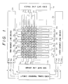
- Fig. 8 shows a schematic construction of the LCD (liquid crystal display) panel.
- 1a, 1b denote an odd gate line driver and an even gate line driver for driving odd gate lines G1, G3, ... ... and even gate lines G2, G4, ... ... of the aforementioned TFT respectively
- 2a, 2b denote an odd source line driver and an even source line driver for driving odd source lines S1, S3, ... ... and even source lined S2, S4, ... ... of the TFT respectively
- a pixel is formed at intersection of each gate line and source line.
- the invention has been done in view of such problem as mentioned, and its object is to provide a liquid crystal color TV whereby a predetermined color picture is obtainable through driving LCD panel even in the case of interlacing drive to say nothing of the case where R, G, B color filters are arrayed mosaically.
- the liquid crystal color TV of the invention comprises providing a video signal transfer circuit for sampling and transferring each chrominance signal of red, green and blue separated from a video signal at a predetermined period at every horizontal scanning time and also at every field, driving on matrix a plurality of liquid crystal cells with red, green and blue color filters arrayed in a predetermined pattern according to an output of the transfer circuit.
- each chrominance signal of R, G, B separated from a video signal is sampled and transferred at a predetermined period at every horizontal scanning time and also at every field. Then, liquid crystal cells are driven on each transferred chrominance signal.
- LCD panel can be driven even in case R, G, B color filters are arrayed mosaically, and is also to cope with the case of interlacing drive.
- Fig. 1 is a schematic block diagram of LCD panel for a liquid crystal color television relating to the invention
- Fig. 2 is a detailed drawing showing the interior of panel of Fig. 1
- Fig. 3 is a concrete circuit diagram of a video signal transfer circuit
- Fig. 4 (a), (b) are block diagrams showing in detail a multiplexer of Fig. 3
- Fig. 5 is a waveform drawing showing a sampling timing of chrominance signal
- Fig. 6 is a block diagram showing in detail a source line driver
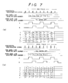
- Fig. 7 (a), (b) are time charts showing a transfer mode of chrominance signals
- Fig. 8 is a block diagram showing a prior art.
- Fig. 1 shows a schematic construction of LCD panel, wherein LCD panel has an odd gate line driver 1a, an even gate line driver 1b, an odd source line driver 2a and an even source line driver 2b, as in the case of prior art, and comprises feeding signals to each pixel at every odd number and even number through gate lines G1, G2, ... ... and source lines S1, S2, ... ... of TFT. Then, R, G, B color filters are arrayed mosaically as illustrated correspondingly to electrodes of each pixel formed at intersections of the gate lines G1, G2, ... ... and the source lines S1, S2, ... ... .
- a video signal transfer circuit 3 for sampling and transferring each chrominance signal of R, G, B separated from a video signal at a predetermined period at every horizontal scanning time and also at every field is provided thereon, video signals (a, b, c, a′, b′, c′) output from the transfer circuit 3 are fed to the source line drivers 2a, 2b through input terminals V A1 , V B1 , V C1 , V A2 , V B2 , V C2 , respectively, and thus each liquid crystal cell is driven on matrix.
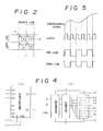
- Fig. 2 is a drawing showing a construction of the interior of the aforementioned panel in detail.
- TFT 4 and R, G, B color filter 5 are arrayed on each pixel at the intersection of each gate line and source line, and each liquid crystal display cell is driven on matrix.
- Fig. 3 is a concrete circuit diagram of the video signal transfer circuit 3.
- the circuit 3 is provided with amplifiers 6a, 6b for amplifying each chrominance signal of R, G, B (signal separated from the video signals) inputted from input terminals I1 to I3 to a predetermined voltage, namely a voltage capable of driving the liquid crystals, six multiplexers U1 to U6 for transferring analog signals output from the amplifiers 6a, 6b, and the multiplexers U1 to U6 are controlled on a 2-bit control signal from input terminals I4, I5 and INHIBIT signal from input terminals I6, I7.
- the aforementioned 2-bit control signal becomes an output signal from a ternary counter concretely.
- each chrominance signal of R, G, B can be transferred and output to the source line drivers 2a, 2b of Fig. 1 from output terminals O1 to O6.
- Each multiplexer is shown in detail in Fig. 4.
- the multiplexer comprises a converter for converting a logic level of output signals (A, B) of the aforementioned ternary counter and inhibit signal (INH), a decoder and a switch unit.
- Each chrominance signal of R, G, B separated from the video signals is inputted to the source line drivers 2a, 2b through the video signal transfer circuit 3, sampled at every three lines here and then fed to each source line.
- chrominance signals inputted from the terminals V B1 , V B2 are sampled at every 3n - 1 lines
- signals inputted from V C1 , V C2 are sampled at every 3n lines and then output.
- the source lines are divided into odd lines and even lines to lower a sampling frequency, and sampling clocks are assigned half each as shown in Fig. 5.
- Fig. 6 shows the source line drivers 2a, 2b in detail.
- the video signals a, b, c from the video signal transfer circuit 3 which are amplified to a voltage capable of driving the liquid crystals are sampled by a buffer BF.
- a switch SW is operated every time a data (horizontal scanning start pulse) STH is shifted by a 60-bit shift register SR on a shift clock CPH, and the video signals a, b, c (a′, b′, c′) are fed to the buffer BF to sampling.
- the switch SW is provided correspondingly to each video signal in this case, and outputs (D1, D2, ...
- LS denotes a level shifter
- PS denotes a power unit capable of adjusting a luminance of the liquid crystals
- a plurality of powers (V b , V BB1 to V BB3 , V DD , V SS ) different in voltage are fed externally to the circuit.
- signals R, B, G are inputted to a terminal V A1 of the odd source line driver 2a, a terminal V B1 and a terminal V C1 respectively, while signals G, R, B are inputted to a terminal V A2 of the even source line driver 2b, a terminal V B2 and a terminal V C2 respectively.
- signals proper for each color filter can be fed to each pixel.
- a gate line G3 will be turned on at the next horizontal scanning time, therefore signals corresponding thereto must be fed to each terminal of the source line drivers 2a, 2b.
- signals R, G, B are transferred on the video signal transfer circuit 3 shown in Fig. 3. That is, the circuit has 2-bit control signals A, B and an inhibit signal inputted by six analog multiplexers U1 to U6, and controls two sets of 3 channels on a 2-bit signal.
- the signals a, b, c and a′, b′, c′ be transferred to any of the signals R, G, B, as described hereinbefore, at every horizontal scanning time and also at every field, and thus outputs of the ternary counter are inputted to the multiplexers U1 to U6 as the control signals A, B.
- a source signal corresponding to the gate line G1 is fed at the horizontal scanning time before the first gate line G1 is turned on, therefore a display action starts before the gate line G1 is turned on.
- the control signals A and B are kept at "H” and "L” respectively, and 1X terminal and XCOM terminal, 1Y terminal and YCOM terminal of the multiplexers U1 to U6 are conductive each, therefore the signals G and R are inputted to 1X terminal and 1Y terminal of the multiplexer U1 respectively, the signals B and R′ are inputted to 1Y terminal and 1X terminal of the multiplexer U3, and the signals B and G are inputted to 1X terminal and 1Y terminal of the multiplexer U5 respectively.
- the control signals A, B are output signals of the ternary counter, the signals A, B are kept at "L” both, and the aforementioned operation is repeated.
- Fig. 7 (a) and (b) are time charts showing a mode wherein signals in the aforementioned odd field and even field are transferred. As illustrated, each gate line is selected at rise of a horizontal synchronizing pulse, and signals R, G, B (R′, G′, B′) are fed at every field.
- LCD panel of interlacing drive can be driven through a simple construction utilizing analog multiplexers, and a predetermined color picture is obtainable even in case color filters are arrayed in a mosaic pattern. Then, an array other than the mosaic patter is also available by changing the order of video signals inputted to each multiplexer.
- a video signal transfer circuit for sampling and transferring each chrominance signal of R, G, B which is separated from video signals at a predetermined period at every horizontal scanning time and also at every field is provided, a predetermined color picture is obtainable through driving LCD panel of interlacing drive even in case R, G, B color filters are arrayed mosaically.
Landscapes
- Engineering & Computer Science (AREA)
- Chemical & Material Sciences (AREA)
- Crystallography & Structural Chemistry (AREA)
- Physics & Mathematics (AREA)
- Computer Hardware Design (AREA)
- General Physics & Mathematics (AREA)
- Theoretical Computer Science (AREA)
- Multimedia (AREA)
- Signal Processing (AREA)
- Liquid Crystal Display Device Control (AREA)
- Video Image Reproduction Devices For Color Tv Systems (AREA)
Applications Claiming Priority (2)
| Application Number | Priority Date | Filing Date | Title |
|---|---|---|---|
| JP305540/87 | 1987-12-04 | ||
| JP30554087A JPH01147988A (ja) | 1987-12-04 | 1987-12-04 | 液晶カラーテレビジョン |
Publications (2)
| Publication Number | Publication Date |
|---|---|
| EP0320562A1 true EP0320562A1 (fr) | 1989-06-21 |
| EP0320562B1 EP0320562B1 (fr) | 1993-05-12 |
Family
ID=17946388
Family Applications (1)
| Application Number | Title | Priority Date | Filing Date |
|---|---|---|---|
| EP19880103093 Expired - Lifetime EP0320562B1 (fr) | 1987-12-04 | 1988-03-01 | Télévision en couleur à cristaux liquides |
Country Status (3)
| Country | Link |
|---|---|
| EP (1) | EP0320562B1 (fr) |
| JP (1) | JPH01147988A (fr) |
| DE (1) | DE3880985T2 (fr) |
Cited By (2)
| Publication number | Priority date | Publication date | Assignee | Title |
|---|---|---|---|---|
| EP0554051A1 (fr) * | 1992-01-31 | 1993-08-04 | Canon Kabushiki Kaisha | Dispositif d'affichage d'images avec une couche de silicium monocristallin et procédés de fabrication et de commande |
| EP0637009A3 (fr) * | 1993-07-30 | 1997-03-19 | Canon Kk | Procédé et dispositif de commande pour un affichage couleur à cristaux liquides avec matrice active. |
Citations (4)
| Publication number | Priority date | Publication date | Assignee | Title |
|---|---|---|---|---|
| EP0158366A2 (fr) * | 1984-04-13 | 1985-10-16 | Sharp Kabushiki Kaisha | Dispositif d'affichage à cristal liquide en couleurs |
| EP0167408A2 (fr) * | 1984-07-06 | 1986-01-08 | Sharp Kabushiki Kaisha | Circuit de commande pour un dispositif d'affichage en couleurs à cristaux liquides |
| GB2162674A (en) * | 1984-06-22 | 1986-02-05 | Citizen Watch Co Ltd | Color liquid crystal display apparatus with improved display color mixing |
| EP0186086A2 (fr) * | 1984-12-17 | 1986-07-02 | Canon Kabushiki Kaisha | Panneau d'affichage en couleurs |
Family Cites Families (1)
| Publication number | Priority date | Publication date | Assignee | Title |
|---|---|---|---|---|
| JPH0631925B2 (ja) * | 1984-03-29 | 1994-04-27 | 三菱電機株式会社 | カラ−表示装置 |
-
1987
- 1987-12-04 JP JP30554087A patent/JPH01147988A/ja active Pending
-
1988
- 1988-03-01 EP EP19880103093 patent/EP0320562B1/fr not_active Expired - Lifetime
- 1988-03-01 DE DE19883880985 patent/DE3880985T2/de not_active Expired - Fee Related
Patent Citations (4)
| Publication number | Priority date | Publication date | Assignee | Title |
|---|---|---|---|---|
| EP0158366A2 (fr) * | 1984-04-13 | 1985-10-16 | Sharp Kabushiki Kaisha | Dispositif d'affichage à cristal liquide en couleurs |
| GB2162674A (en) * | 1984-06-22 | 1986-02-05 | Citizen Watch Co Ltd | Color liquid crystal display apparatus with improved display color mixing |
| EP0167408A2 (fr) * | 1984-07-06 | 1986-01-08 | Sharp Kabushiki Kaisha | Circuit de commande pour un dispositif d'affichage en couleurs à cristaux liquides |
| EP0186086A2 (fr) * | 1984-12-17 | 1986-07-02 | Canon Kabushiki Kaisha | Panneau d'affichage en couleurs |
Non-Patent Citations (1)
| Title |
|---|
| IEEE TRANSACTIONS ON CONSUMER ELECTRONICS, vol. CE-31, no. 1, February 1985, pages 39-45, IEEE, New York, US; M. YAMANO et al.: "The 5- inch size full color liquid crystal television addressed by amorphous silicon thin film transistors" * |
Cited By (3)
| Publication number | Priority date | Publication date | Assignee | Title |
|---|---|---|---|---|
| EP0554051A1 (fr) * | 1992-01-31 | 1993-08-04 | Canon Kabushiki Kaisha | Dispositif d'affichage d'images avec une couche de silicium monocristallin et procédés de fabrication et de commande |
| EP0637009A3 (fr) * | 1993-07-30 | 1997-03-19 | Canon Kk | Procédé et dispositif de commande pour un affichage couleur à cristaux liquides avec matrice active. |
| US5619225A (en) * | 1993-07-30 | 1997-04-08 | Canon Kabushiki Kaisha | Liquid crystal display apparatus and method of driving the same |
Also Published As
| Publication number | Publication date |
|---|---|
| JPH01147988A (ja) | 1989-06-09 |
| EP0320562B1 (fr) | 1993-05-12 |
| DE3880985T2 (de) | 1993-09-02 |
| DE3880985D1 (de) | 1993-06-17 |
Similar Documents
| Publication | Publication Date | Title |
|---|---|---|
| KR100242443B1 (ko) | 도트 반전 구동을 위한 액정 패널 및 이를 이용한 액정 표시 장치 | |
| US6049321A (en) | Liquid crystal display | |
| KR100945581B1 (ko) | 액정 표시 장치 및 그 구동 방법 | |
| EP0466378B1 (fr) | Panneau d'affichage à cristal liquide avec scintillement réduit | |
| EP1052615B1 (fr) | Méthode de commande d'un affichage à panneau plat | |
| JP3621982B2 (ja) | 薄膜トランジスタ液晶表示装置と駆動方法及び駆動装置 | |
| EP0368572B1 (fr) | Dispositif et méthode de commande d'un panneau d'affichage à cristaux liquides | |
| KR100312755B1 (ko) | 멀티싱크를 위한 액정 표시 장치 및 디스플레이 장치와 각각의 구동 장치 | |
| KR20060021055A (ko) | 액정 표시 장치, 액정 표시 장치용 구동 장치 및 방법 | |
| JPS59111197A (ja) | マトリクス型表示装置の駆動回路 | |
| JPH07109544B2 (ja) | 液晶表示装置並びにその駆動方法及び駆動装置 | |
| KR0142131B1 (ko) | Tft디스플레이장치 | |
| EP0213630B1 (fr) | Dispositif à cristaux liquides et sa méthode de commande | |
| KR20020077036A (ko) | 액정표시장치 및 그 구동회로 | |
| EP0320562A1 (fr) | Télévision en couleur à cristaux liquides | |
| JP4846133B2 (ja) | 駆動回路、電極基板及び液晶表示装置 | |
| JP3491814B2 (ja) | 集積回路装置およびそれを用いた液晶表示装置 | |
| JP2767238B2 (ja) | 液晶表示装置 | |
| JP3804853B2 (ja) | 液晶駆動装置およびその駆動方法 | |
| JPH02312466A (ja) | 液晶ディスプレイ装置 | |
| JP3433022B2 (ja) | 液晶表示装置 | |
| JP2613204B2 (ja) | カラー液晶デイスプレイ装置 | |
| JP3082227B2 (ja) | 液晶カラーディスプレイ装置 | |
| JP2000039872A (ja) | 液晶駆動装置 | |
| JPH0664436B2 (ja) | 画像表示装置 |
Legal Events
| Date | Code | Title | Description |
|---|---|---|---|
| PUAI | Public reference made under article 153(3) epc to a published international application that has entered the european phase |
Free format text: ORIGINAL CODE: 0009012 |
|
| AK | Designated contracting states |
Kind code of ref document: A1 Designated state(s): DE FR GB NL |
|
| 17P | Request for examination filed |
Effective date: 19890724 |
|
| 17Q | First examination report despatched |
Effective date: 19910708 |
|
| GRAA | (expected) grant |
Free format text: ORIGINAL CODE: 0009210 |
|
| AK | Designated contracting states |
Kind code of ref document: B1 Designated state(s): DE FR GB NL |
|
| REF | Corresponds to: |
Ref document number: 3880985 Country of ref document: DE Date of ref document: 19930617 |
|
| ET | Fr: translation filed | ||
| PGFP | Annual fee paid to national office [announced via postgrant information from national office to epo] |
Ref country code: NL Payment date: 19950331 Year of fee payment: 8 |
|
| PG25 | Lapsed in a contracting state [announced via postgrant information from national office to epo] |
Ref country code: NL Effective date: 19961001 |
|
| NLV4 | Nl: lapsed or anulled due to non-payment of the annual fee |
Effective date: 19961001 |
|
| PGFP | Annual fee paid to national office [announced via postgrant information from national office to epo] |
Ref country code: FR Payment date: 19980319 Year of fee payment: 11 |
|
| PGFP | Annual fee paid to national office [announced via postgrant information from national office to epo] |
Ref country code: GB Payment date: 19980325 Year of fee payment: 11 |
|
| PGFP | Annual fee paid to national office [announced via postgrant information from national office to epo] |
Ref country code: DE Payment date: 19980326 Year of fee payment: 11 |
|
| PG25 | Lapsed in a contracting state [announced via postgrant information from national office to epo] |
Ref country code: GB Free format text: LAPSE BECAUSE OF NON-PAYMENT OF DUE FEES Effective date: 19990301 |
|
| GBPC | Gb: european patent ceased through non-payment of renewal fee |
Effective date: 19990301 |
|
| PG25 | Lapsed in a contracting state [announced via postgrant information from national office to epo] |
Ref country code: FR Free format text: LAPSE BECAUSE OF NON-PAYMENT OF DUE FEES Effective date: 19991130 |
|
| REG | Reference to a national code |
Ref country code: FR Ref legal event code: ST |
|
| PG25 | Lapsed in a contracting state [announced via postgrant information from national office to epo] |
Ref country code: DE Free format text: LAPSE BECAUSE OF NON-PAYMENT OF DUE FEES Effective date: 20000101 |
|
| PLBE | No opposition filed within time limit |
Free format text: ORIGINAL CODE: 0009261 |
|
| STAA | Information on the status of an ep patent application or granted ep patent |
Free format text: STATUS: NO OPPOSITION FILED WITHIN TIME LIMIT |