EP0320748B1 - Circuit d'asservissement de phase à autoréglage - Google Patents
Circuit d'asservissement de phase à autoréglage Download PDFInfo
- Publication number
- EP0320748B1 EP0320748B1 EP88120320A EP88120320A EP0320748B1 EP 0320748 B1 EP0320748 B1 EP 0320748B1 EP 88120320 A EP88120320 A EP 88120320A EP 88120320 A EP88120320 A EP 88120320A EP 0320748 B1 EP0320748 B1 EP 0320748B1
- Authority
- EP
- European Patent Office
- Prior art keywords
- voltage
- frequency
- input
- signal
- fvco
- Prior art date
- Legal status (The legal status is an assumption and is not a legal conclusion. Google has not performed a legal analysis and makes no representation as to the accuracy of the status listed.)
- Expired - Lifetime
Links
Images

Classifications
-
- H—ELECTRICITY
- H03—ELECTRONIC CIRCUITRY
- H03L—AUTOMATIC CONTROL, STARTING, SYNCHRONISATION OR STABILISATION OF GENERATORS OF ELECTRONIC OSCILLATIONS OR PULSES
- H03L1/00—Stabilisation of generator output against variations of physical values, e.g. power supply
-
- H—ELECTRICITY
- H03—ELECTRONIC CIRCUITRY
- H03L—AUTOMATIC CONTROL, STARTING, SYNCHRONISATION OR STABILISATION OF GENERATORS OF ELECTRONIC OSCILLATIONS OR PULSES
- H03L7/00—Automatic control of frequency or phase; Synchronisation
- H03L7/06—Automatic control of frequency or phase; Synchronisation using a reference signal applied to a frequency- or phase-locked loop
- H03L7/08—Details of the phase-locked loop
- H03L7/10—Details of the phase-locked loop for assuring initial synchronisation or for broadening the capture range
- H03L7/113—Details of the phase-locked loop for assuring initial synchronisation or for broadening the capture range using frequency discriminator
-
- H—ELECTRICITY
- H03—ELECTRONIC CIRCUITRY
- H03L—AUTOMATIC CONTROL, STARTING, SYNCHRONISATION OR STABILISATION OF GENERATORS OF ELECTRONIC OSCILLATIONS OR PULSES
- H03L2207/00—Indexing scheme relating to automatic control of frequency or phase and to synchronisation
- H03L2207/06—Phase locked loops with a controlled oscillator having at least two frequency control terminals
Definitions
- the present invention relates to a self adjusting phase lock circuit.
- phase lock circuits are used.
- a magnetic media When a magnetic media is read, it produces, through suitable reading circuits, a sequence of electrical pulses having a variable frequency modulated around a nominal frequency.
- Modulation has two components: a logical or meaningfull modulation and a noise modulation caused by changes of the magnetic media speed as to a nominal speed.
- phase lock circuits which basically comprise:
- phase comparator, phase discriminator, the integrating network and the voltage controlled oscillator form a feedback frequency control system for the oscillator, where the control voltage for the oscillator consists in the voltage output by the integrating network and the controlled variable is the variable frequency signal output by the oscillator and input to the phase comparator/discriminator. Since the digital information read out from a magnetic media consists in a plurality of intermittent bit streams, means are further provided to impose a self run condition to the phase lock circuit when the bit stream is missing.
- the voltage controlled oscillator is caused to generate an output signal having a frequency close to a predetermined reference frequency.
- the document JP-A-5260052 discloses the addition to the basic components of the phase lock circuit of a reference frequency generator, a frequency comparator for comparing the frequency of the signal generated by the voltage controlled oscillator with the frequency of the signal generated by the reference frequency generator, a first switch for controlling the inputing of an error signal generated by the frequency comparator to the input of the integrating network and a sample and hold circuit, coupled by a second switch to the output of the integrating network, for periodically storing the control voltage in output from the integrating network, which causes, when applied to the input of the voltage controlled oscillator, the VCO running at the reference frequency.
- the sample and hold circuit then "adds" this signal to the control error signal generated under normal operative conditions in which the bit stream is present.
- phase comparators as well as voltage controlled oscilllators are available on the market in form of integrated circuits, for instance of the types manufactured by the firm Signetics, with code SCB58459 and by the firm Texas Instruments with Code SN74LS629 respectively.
- the voltage controlled oscillator is a critical element of this control system.
- VRANGE defines by its value the proportionality coefficient which relates the control voltage to the output frequency.
- a predetermined output frequency must correspond to a predetermined input control voltage, centered in the admissible control voltage range. Further the set point must not drift with temperature changes.
- suitable adjusting circuits comprising trimming resistors and positive temperature coefficient thermistors (PCT) which provide at the adjusting input a range voltage VRANGE suitable for ech particular unit and variable with the temperature so as to compensate for spread and drift in the operation of the used component.
- PCT positive temperature coefficient thermistors
- phase lock circuit of the present invention in which it is the control circuit itself which periodically provides to generate and adjust the range voltage as a function of the actual response of the used component.
- the invention consists in providing circuit elements which enable the phase lock circuit to operate in self adjusting mode.
- phase lock circuit When the phase lock circuit is in self adjusting mode, a predetermined voltage, corresponding to the desired set point is input to the control input of the oscillator and the output frequency is compared with a reference frequency, corresponding to a desired output frequency.
- An error signal is generated which modifies the range voltage VRANGE input to the oscillator.
- This operative mode may be periodically imposed at fixed time periods, or when the phase lock circuit is idle, in particular, for phase lock circuits working in magnetic disk units, when the reading head is moving from one track to another.
- the purpose of the invention is to set the operation of the voltage controlled oscillator for optimal performances. This is obtained by applying to the control input of the VCO a predetermined voltage and by correcting the range voltage VRANGE so that the VCO runs at the reference frequency.
- the circuits used to obtain this result are similar, at some extent, to the circuits disclosed by document JP-A-5260052, but the purpose and the arrangement of the several elements are entirely different.
- the circuit comprises a frequency comparator 1, a voltage controlled oscillator 2, an integrating network consisting in resistor 3 and capacitor 4, an operational amplifier 5 having unit gain, a thermistor 6 and a voltage divider 7.
- Comparator 1 receives as inputs a RD signal, frequency modulated, consisting in a sequence of electrical pulses read out from a magnetic media, and a FVCO square wave signal, having variable frequency which is the output from oscillator 2.
- comparator 1 may be implemented in several ways, including analogic circuits, digital comparators are preferably used because of their intrinsic precision and stability.
- the output of comparator 1 is an error signal E consisting in electrical pulses having alternatively a level +V (the Voltage supply of Comparator 1) or level 0 and duration variable as a function of the frequency error of the RD signal as to the FVCO signal in input.
- the output pulses at level +V have the same width of the output pulses at level 0. If the RD signal frequency is greater than the FVCO signal frequency, the pulses at level +V have a width greater than the one of the pulses at level 0 and viceversa if the RD signal frequency is lesser than the FVCO signal frequency.
- Some comparators produce at the output (or at two distinct outputs) pulses at level +V or at level 0 in mutual exclusive way, depending on the frequency of signal RD being greater or lesser than FVCO.
- the effect of the error pulses input to the integrating network is to load capacitor 4 at a variable voltage level.
- the charge voltage of capacitor 4 is + V/2.
- the charge voltage will be greater than +V/2 and lesser if RD has a frequency lesser than FVCO.
- Voltage +V/2 is the normal working point of the control system. It defines the operative conditions of the system when there is no error.
- the charge voltage of capacitor 4, referenced as VC, is input to the control input of voltage controlled oscillator 2, through operational amplifier 5, having unit gain.
- the function of operational amplifier 5 is only to decouple capacitor 4 from the input impedance of oscillator 2, which input is relatively low.
- an operational amplifier has a virtually infinite input impedance. As a consequence it does not drain current from capacitor 4 and does not alter the electrical status of the integrating network.
- Voltage VRANGE is preferably obtained from a voltage divider 7 and a PCT 6, series connected between voltage source +V and ground.
- the center tap of voltage divider 7 is connected to the adjusting input of oscillator 2.
- the adjusting input may therefore receive a voltage comprised between 0V and a voltage close to +V.
- VRANGE which corresponds to a predetermined VC equal to +V/2 and to an output frequencyFVCO equal to the nominal value of the input frequency of RD signal.
- K1 is variable from unit component to unit component and further with temperature.
- An adjusting operation is therefore required, in the manufacturing or maintenance of the described circuits, which implies, at a predetermined temperature, the inputing of a known reference frequency FR as a substitute for RD, such frequency corresponding to the nominal frequency of RD, and to adjust the position of the voltage divider 7 cursor, until the frequency of signal FVCO equals the reference one.
- the adjusting operation compensates for performance spreads of the oscillator components and assures a correct working point to the control system at the moment and in the adjustment environment. It does not assures that the set point is maintained with time and at differing temperatures.
- the use of a PCT thermistor compensates only in part for thermal drift.
- Figures 2 and 3 show the same circuit in normal operating mode and in self adjusting mode respectively.
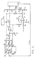
- the circuit of figure 2 comprises, in addition to frequency comparator 1, oscillator 2, resistor 3 capacitor 4, amplifier 5, already seen in figure 1 and connected together the same way, an electronic switch (multiplexer) 6, an oscillator 7 for the generation of a reference frequency VR, a second electronic switch 8, a second operational amplifier 9, having function of a subtractor with gain, an electronic switch 10, a capacitor 11 and a third operational amplifier 17, used as a decoupling element with unit gain.
- a disk unit controller 12 provides a control signal which in normal operating read mode maintains the switches in the position shown in figure 2 and in operative adjustment mode maintains the switches in the position shown in figure 3.
- comparator 1 receives as input, through switch 8, signal RD and that capacitor 4 charge voltage VC is input, through amplifier 5 and switch 6, to the control input of oscillator 2.
- Voltage VC is further input to the non inverting input of amplifier 9, through a resistor 13.
- the inverting input of amplifier 9 is connected to a reference voltage V1, through a resistor 14.
- a resistor 15 connects the inverting input to the output.
- the non inverting input is ground connected through resistor 16.
- the output of amplifier 9 is, in figure 2, isolated, owing to switch 10 being open, whilst in figure 3 is closed, through switch 10, on capacitor 11 and on input of amplifier 17, whose output is connected to the adjusting input of oscillator 2.
- phase lock circuit operates in the same way of the circuit of figure 1, the only difference being that the voltage VRANGE in input to the oscillator is the charge voltage of capacitor 11.
- Figure 3 shows how voltage VRANGE is obtained in the self adjusting operation mode.
- switch 6 connects the control input of oscillator 2 to a fixed voltage source +V/2 corresponding to the nominal working point or set point, and switch 8 connects the input of comparator 1 to the output of oscillator 7.
- the integrating network produces a signal VC related to the frequency error between FR and FVCO.
- Signal VC is input to amplifier 9 which outputs to capacitor 11 and to the adjusting input of oscillator 2 (through switch 10 which is closed) a voltage VRANGE obtained according to the following transfer function.
- VRANGE (V1-VC) ⁇ K3 where K3 is a gain coefficient defined by the ratio between the value of feedback and biasing resistors of amplifier 9.
- Values for K3 and V1 may be suitably choosen in relation to the voltage supply for components 1,2 and the admissible voltage range for VRANGE.
- VRANGE spans from +5V to 0V.
- the control loop so formed provides to load capacitor 11 and to input to the adjusting input of oscillator 2 a voltage VRANGE which establishes a stable state in which the offset of VC from the set point is minimum as well as the offset of FVCO from the reference frequency FR.
- the charge level is maintained substantially unchanged for periods in the order of hundreds of msec. This is because the input impedance of amplifer 17 is virtually infinite.
- the circuit automatically provides to change voltage VRANGE so as to establish a working point which differs from the nominal point for a minimal amount.
- the preferred embodiment makes use of circuit components easily available on the market and provides some circuital simplification.
- the phase lock circuit comprises a comparator/ discriminator 20, consisting in an integrated circuit SCB68459 and a controlled oscillator 2 consisting in integrated circuit 74LS629, already mentioned.
- Comparator 20 has two inputs X1,X2 for connection to an external oscillator 21, which produces a reference signal FR having a frequency twice the nominal working frequency, that is the nominal frequency of read signal RD.
- Comparator 20 receives signal RD at one input 22 and signal FVCO at an input 23.
- Circuit 20 comprises "de facto" two distinct comparators:
- Output 24 is connected to a first armature of a capacitor 27, through a resistor 28.
- the second armature of capacitor 27 is grounded.
- Output 25 is connected to the first armature of capacitor 27 through a resistor 29, series connected with an electronic switch 31.
- Output 26 is connected to the first armature of capacitor 27 through a resistor 30, series connected with the electronic switch 31.
- Resistors 28,29,30 and capacitor 27 form an integrating network in which signal PUP tends to charge capacitor 27, signal PDOWN tends to discharge capacitor 27 and signal FPUMP tends to charge or discharge capacitor 27 depending on FVCO having a frequency lesser or greater that FR.
- capacitor 27 When switch 31 is closed, capacitor 27 is charged at a voltage level related to the phase error of RD as to FVCO and corrected as a function of the frequency error of FVCO as to FR.
- capacitor 27 When switch 31 is open, capacitor 27 is powered by FPUMP signal only and is charged at a voltage level related to the frequency error of FVCO as to FR.
- the first armature of capacitor 27 is connected to the non inverting input of operational amplifier 32, operating as a voltage follower with high input impedance, hence as a simple decoupler.
- the output of amplifier 32 is connected to the control input of oscillator 2, through an electronic switch 33.
- the output of amplifier 32 is connected to the inverting input of operational amplifier 37, through a resistor 36.
- the non-inverting input of amplifier 37 is connected to the voltage source +V, through a resistor 38, and to ground, through a resistor 39.
- a feedback resistor 40 connects the output to the non inverting input.
- the output of operational amplifier 37 is connected to the first armature of a capacitor 41, through an electronic switch 42.
- the second armature of capacitor 41 is grounded.
- the first armature is further connected, through an operational amplifier 43 having unit gain, to the adjusting input of controlled oscillator 2.
- Electronic switches 31,32,42 are for instance analogic switches marketed by the firm National with code MM74HC4066, whilst the operational amplifiers may be those marketed by firm NATIONAL with code LF347.
- a disk control unit 43 provides control signal CTR to switches 31,33.
- CTR is also input, through inverter 44, to the control input of switch 42.
Landscapes
- Stabilization Of Oscillater, Synchronisation, Frequency Synthesizers (AREA)
Claims (3)
- Circuit à asservissement de phase à auto-réglage, du type comportant des premiers moyens (1,3,4,5) pour comparer la fréquence et/ou la phase d'un signal de référence (FVCO) avec un signal entré périodiquement, (RD), de fréquence variable et pour générer une tension de commande (VC) fonction de l'erreur de fréquence/de phase entre le signal de référence (FVCO) et le signal entré (RD), et comportant en outre- un oscillateur commandé en tension (2) recevant ladite tension de commande VC à une entrée de commande, une tension de réglage (VRANGE) à une entrée de réglage et fournissant ledit signal de référence (FVCO) en fonction de ladite tension de commande (VC) et de ladite tension de réglage (VRANGE),- des seconds moyens (8,1,3,4,5) pour comparer la fréquence dudit signal de référence (FVCO) avec une fréquence de travail nominale (FR) et pour générer une tension fonction de l'erreur entre ladite fréquence de travail nominale (FR) et la fréquence dudit signal de référence (FVCO),
ledit circuit à asservissement de phase étant caractérisé par le fait qu'il comporte:- des troisièmes moyens (6) pour découpler ladite tension de commande (VC) d'avec ladite entrée de commande et pour appliquer à ladite entrée de commande une tension de référence prédéterminée,- des quatrièmes moyens (9,14,15,16), opérant sur la tension générée par lesdits seconds moyens (8,1,3,4,5), pour générer ladite tension de réglage (VRANGE),- des cinquièmes moyens (10,11) pour échantillonner et mémoriser ladite tension de réglage (VRANGE),- des sixièmes moyens (17) à haute impédance d'entrée pour appliquer à ladite entrée de réglage ladite tension de réglage (VRANGE) échantillonnée et mémorisée par lesdits cinquièmes moyens (10,11),- des septièmes moyens (12) pour commander en synchronisme lesdits troisièmes (6) et lesdits cinquièmes (10,11) moyens pour respectivement découpler et échantillonner,
lesdits seconds, quatrièmes, cinquièmes, sixièmes moyens et ledit oscillateur formant une boucle de commande de rétroaction de la fréquence dudit signal de référence (FVCO), boucle dans laquelle ladite tension de réglage (VRANGE) constitue le signal de contrôle d'erreur. - Circuit à asservissement de phase comme revendiqué dans la revendication 1, dans lequel lesdits seconds moyens (8,1,3,4,5) comportent lesdits premiers moyens (1,3,4,5) et de plus des moyens (8) pour substituer ladite fréquence de travail nominale (FR) audit signal entré périodiquement (RD) de fréquence variable, au titre de signal d'entrée desdits premiers moyens.
- Circuit à asservissement de phase comme revendiqué dans la revendication 1, dans lequel lesdits premiers moyens (1,3,4,5) comportent A) un comparateur de phase (20) pour comparer la phase dudit signal de référence (FVCO) avec la phase dudit signal entré périodiquement (RD) et pour générer au moins un premier signal d'erreur de phase (PUP), un comparateur de fréquence (20) pour comparer la fréquence de ladite fréquence de travail nominale (FR) avec la fréquence dudit signal de référence (FVCO) et pour générer un signal d'erreur de fréquence (FPUMP), et B) un réseau intégrateur (28,30,27) de ladite première erreur de phase et de ladite erreur de fréquence pour générer une tension d'erreur (VC) fonction de ladite erreur de phase et de ladite erreur de fréquence, et circuit dans lequel- lesdits troisièmes moyens (6) comportent un premier commutateur analogique (33) et un diviseur de tension (34,35) relié à la sortie dudit premier commutateur (33),- lesdits seconds moyens comportent ledit comparateur de fréquence (20), ledit réseau intégrateur (28,30,27) et une second commutateur analogique (31) pour découpler ledit premier signal d'erreur de phase d'avec l'entrée dudit réseau intégrateur,- lesdits quatrièmes moyens comportent un premier amplificateur opérationnel (37) qui effectue, avec gain, l'opération consistant à soustraire d'une tension de référence la tension générée par lesdits troisièmes moyens, et- lesdits cinquièmes moyens comportent un troisième commutateur analogique (42) relié à la sortie dudit premier amplificateur opérationnel (37) et un condensateur (41) relié entre la sortie dudit troisième commutateur et la masse.
Applications Claiming Priority (2)
| Application Number | Priority Date | Filing Date | Title |
|---|---|---|---|
| IT2307887 | 1987-12-18 | ||
| IT23078/87A IT1223524B (it) | 1987-12-18 | 1987-12-18 | Circuito ad aggancio di fase autotarante |
Publications (3)
| Publication Number | Publication Date |
|---|---|
| EP0320748A2 EP0320748A2 (fr) | 1989-06-21 |
| EP0320748A3 EP0320748A3 (en) | 1989-09-13 |
| EP0320748B1 true EP0320748B1 (fr) | 1993-02-17 |
Family
ID=11203541
Family Applications (1)
| Application Number | Title | Priority Date | Filing Date |
|---|---|---|---|
| EP88120320A Expired - Lifetime EP0320748B1 (fr) | 1987-12-18 | 1988-12-06 | Circuit d'asservissement de phase à autoréglage |
Country Status (4)
| Country | Link |
|---|---|
| US (1) | US4918404A (fr) |
| EP (1) | EP0320748B1 (fr) |
| DE (1) | DE3878539T2 (fr) |
| IT (1) | IT1223524B (fr) |
Families Citing this family (17)
| Publication number | Priority date | Publication date | Assignee | Title |
|---|---|---|---|---|
| US5029237A (en) * | 1988-06-30 | 1991-07-02 | At&E Corporation | Radio receiver frequency control system |
| NL8802868A (nl) * | 1988-11-21 | 1990-06-18 | Stichting Tech Wetenschapp | Fasevergrendelde lus met lusversterking - en nulpuntscompensatie. |
| US5214310A (en) * | 1990-11-29 | 1993-05-25 | Emerson Electric Co. | Timing mechanism with a PTC thermistor |
| US5260979A (en) * | 1991-05-28 | 1993-11-09 | Codex Corp. | Circuit and method of switching between redundant clocks for a phase lock loop |
| US5604466A (en) * | 1992-12-08 | 1997-02-18 | International Business Machines Corporation | On-chip voltage controlled oscillator |
| JPH06197014A (ja) * | 1992-12-25 | 1994-07-15 | Mitsubishi Electric Corp | 位相同期回路 |
| FI97003C (fi) * | 1993-09-27 | 1996-09-25 | Nokia Telecommunications Oy | Menetelmä vaihelukitun silmukan ohjaamiseksi sekä vaihelukittu silmukka |
| US5642069A (en) * | 1994-04-26 | 1997-06-24 | Unisys Corporation | Clock signal loss detection and recovery apparatus in multiple clock signal system |
| US5559473A (en) * | 1994-06-23 | 1996-09-24 | At&T Global Information Solutions Company | Multi-range voltage controlled oscillator |
| US5477198A (en) * | 1994-06-23 | 1995-12-19 | At&T Global Information Solutions Company | Extendible-range voltage controlled oscillator |
| US5748050A (en) * | 1996-03-29 | 1998-05-05 | Symbios Logic Inc. | Linearization method and apparatus for voltage controlled oscillator |
| JPH10257041A (ja) * | 1997-03-11 | 1998-09-25 | Sony Corp | フェイズロックドループ回路及び再生装置 |
| JP3327271B2 (ja) * | 1999-11-15 | 2002-09-24 | 日本電気株式会社 | Pll回路及びデータ読み出し回路 |
| DE10255863B4 (de) * | 2002-11-29 | 2008-07-31 | Infineon Technologies Ag | Phasenregelschleife |
| US20070260771A1 (en) * | 2006-04-10 | 2007-11-08 | Cheng-Hao Lee | Method of Reducing Clock Differential in a Data Processing System |
| US20110033174A1 (en) * | 2009-08-06 | 2011-02-10 | Grenergy Opto, Inc. | Control circuit for a variable frequency dc motor |
| US8248167B2 (en) * | 2010-06-28 | 2012-08-21 | Mstar Semiconductor, Inc. | VCO frequency temperature compensation system for PLLs |
Family Cites Families (6)
| Publication number | Priority date | Publication date | Assignee | Title |
|---|---|---|---|---|
| JPS5260052A (en) * | 1975-11-12 | 1977-05-18 | Fujitsu Ltd | Phase control circuit featuring self-run frequency setting medium |
| US4246545A (en) * | 1979-02-02 | 1981-01-20 | Burroughs Corporation | Data signal responsive phase locked loop using averaging and initializing techniques |
| US4365211A (en) * | 1980-10-31 | 1982-12-21 | Westinghouse Electric Corp. | Phase-locked loop with initialization loop |
| CA1247202A (fr) * | 1984-06-11 | 1988-12-20 | John M. Yarborough | Detecteur de phase et circuit d'asservissement de phase comprenant un tel detecteur |
| US4703520A (en) * | 1986-10-31 | 1987-10-27 | Motorola, Inc. | Radio transceiver having an adaptive reference oscillator |
| IT1197969B (it) * | 1986-11-12 | 1988-12-21 | Honeywell Inf Systems | Circuito ad aggancio di fase |
-
1987
- 1987-12-18 IT IT23078/87A patent/IT1223524B/it active
-
1988
- 1988-09-22 US US07/248,004 patent/US4918404A/en not_active Expired - Fee Related
- 1988-12-06 DE DE8888120320T patent/DE3878539T2/de not_active Expired - Fee Related
- 1988-12-06 EP EP88120320A patent/EP0320748B1/fr not_active Expired - Lifetime
Also Published As
| Publication number | Publication date |
|---|---|
| EP0320748A3 (en) | 1989-09-13 |
| IT1223524B (it) | 1990-09-19 |
| US4918404A (en) | 1990-04-17 |
| DE3878539D1 (de) | 1993-03-25 |
| EP0320748A2 (fr) | 1989-06-21 |
| IT8723078A0 (it) | 1987-12-18 |
| DE3878539T2 (de) | 1993-08-19 |
Similar Documents
| Publication | Publication Date | Title |
|---|---|---|
| EP0320748B1 (fr) | Circuit d'asservissement de phase à autoréglage | |
| US5363419A (en) | Dual phase-locked-loop having forced mid range fine control zero at handover | |
| US5477180A (en) | Circuit and method for generating a clock signal | |
| US5302919A (en) | VCO having voltage-to-current converter and PLL using same | |
| US5247241A (en) | Frequency and capacitor based constant current source | |
| US5909150A (en) | System and method for improving the regulation of a supply voltage for a controllable oscillator using feed forward control techniques | |
| EP0477694A2 (fr) | Méthode et circuit d'accord d'un filtre à temps continu | |
| US4309649A (en) | Phase synchronizer | |
| GB2194402A (en) | Automatic adjustment circuit for a filter | |
| KR101346385B1 (ko) | 누설 보상된 디지털/아날로그 컨버터 | |
| US4625156A (en) | Control device | |
| US5317287A (en) | Low-gain, range programmable, temperature compensated voltage controlled ring oscillator | |
| US4835481A (en) | Circuit arrangement for generating a clock signal which is synchronous in respect of frequency to a reference frequency | |
| US6242956B1 (en) | Phase locked loop | |
| US4945311A (en) | Electronically variable equalizer | |
| US4570130A (en) | Input controller circuit apparatus for phase lock loop voltage controlled oscillator | |
| CA2196998C (fr) | Circuit d'extraction de signaux d'hologe integrable | |
| US5210509A (en) | Dual loop phase locked circuit with sweep generator and compensation for drift | |
| EP0670499B1 (fr) | Convertisseur de tension en fréquence | |
| US4947102A (en) | Feedback loop gain compensation for a switched resistor regulator | |
| GB2288502A (en) | Voltage controlled oscillator | |
| GB2138231A (en) | Signal transmission circuit | |
| US5654675A (en) | Fully integrable phase locked loop with low jitter | |
| EP0168157B1 (fr) | Système de traitement d'un signal de chrominance | |
| KR100526386B1 (ko) | 자동적인 초기화 및 차단에 의해서 위상 동기 루프를 로크 상태로 스위핑시키기 위한 시스템 |
Legal Events
| Date | Code | Title | Description |
|---|---|---|---|
| PUAI | Public reference made under article 153(3) epc to a published international application that has entered the european phase |
Free format text: ORIGINAL CODE: 0009012 |
|
| AK | Designated contracting states |
Kind code of ref document: A2 Designated state(s): DE FR GB NL |
|
| PUAL | Search report despatched |
Free format text: ORIGINAL CODE: 0009013 |
|
| AK | Designated contracting states |
Kind code of ref document: A3 Designated state(s): DE FR GB NL |
|
| 17P | Request for examination filed |
Effective date: 19891216 |
|
| 17Q | First examination report despatched |
Effective date: 19911223 |
|
| GRAA | (expected) grant |
Free format text: ORIGINAL CODE: 0009210 |
|
| AK | Designated contracting states |
Kind code of ref document: B1 Designated state(s): DE FR GB NL |
|
| PG25 | Lapsed in a contracting state [announced via postgrant information from national office to epo] |
Ref country code: NL Effective date: 19930217 |
|
| REF | Corresponds to: |
Ref document number: 3878539 Country of ref document: DE Date of ref document: 19930325 |
|
| ET | Fr: translation filed | ||
| NLV1 | Nl: lapsed or annulled due to failure to fulfill the requirements of art. 29p and 29m of the patents act | ||
| PGFP | Annual fee paid to national office [announced via postgrant information from national office to epo] |
Ref country code: DE Payment date: 19931021 Year of fee payment: 6 |
|
| PLBE | No opposition filed within time limit |
Free format text: ORIGINAL CODE: 0009261 |
|
| STAA | Information on the status of an ep patent application or granted ep patent |
Free format text: STATUS: NO OPPOSITION FILED WITHIN TIME LIMIT |
|
| PGFP | Annual fee paid to national office [announced via postgrant information from national office to epo] |
Ref country code: FR Payment date: 19931224 Year of fee payment: 6 |
|
| 26N | No opposition filed | ||
| PGFP | Annual fee paid to national office [announced via postgrant information from national office to epo] |
Ref country code: GB Payment date: 19941128 Year of fee payment: 7 |
|
| PG25 | Lapsed in a contracting state [announced via postgrant information from national office to epo] |
Ref country code: FR Effective date: 19950831 |
|
| PG25 | Lapsed in a contracting state [announced via postgrant information from national office to epo] |
Ref country code: DE Effective date: 19950901 |
|
| REG | Reference to a national code |
Ref country code: FR Ref legal event code: ST |
|
| PG25 | Lapsed in a contracting state [announced via postgrant information from national office to epo] |
Ref country code: GB Effective date: 19951206 |
|
| GBPC | Gb: european patent ceased through non-payment of renewal fee |
Effective date: 19951206 |