EP0320883A2 - FM-Empfängerschaltung - Google Patents
FM-Empfängerschaltung Download PDFInfo
- Publication number
- EP0320883A2 EP0320883A2 EP88120820A EP88120820A EP0320883A2 EP 0320883 A2 EP0320883 A2 EP 0320883A2 EP 88120820 A EP88120820 A EP 88120820A EP 88120820 A EP88120820 A EP 88120820A EP 0320883 A2 EP0320883 A2 EP 0320883A2
- Authority
- EP
- European Patent Office
- Prior art keywords
- signal
- circuit
- producing
- pass filter
- operative
- Prior art date
- Legal status (The legal status is an assumption and is not a legal conclusion. Google has not performed a legal analysis and makes no representation as to the accuracy of the status listed.)
- Granted
Links
Images

Classifications
-
- H—ELECTRICITY
- H04—ELECTRIC COMMUNICATION TECHNIQUE
- H04L—TRANSMISSION OF DIGITAL INFORMATION, e.g. TELEGRAPHIC COMMUNICATION
- H04L27/00—Modulated-carrier systems
- H04L27/10—Frequency-modulated carrier systems, i.e. using frequency-shift keying
- H04L27/14—Demodulator circuits; Receiver circuits
-
- H—ELECTRICITY
- H04—ELECTRIC COMMUNICATION TECHNIQUE
- H04B—TRANSMISSION
- H04B1/00—Details of transmission systems, not covered by a single one of groups H04B3/00 - H04B13/00; Details of transmission systems not characterised by the medium used for transmission
- H04B1/06—Receivers
- H04B1/16—Circuits
- H04B1/1646—Circuits adapted for the reception of stereophonic signals
- H04B1/1661—Reduction of noise by manipulation of the baseband composite stereophonic signal or the decoded left and right channels
- H04B1/1669—Reduction of noise by manipulation of the baseband composite stereophonic signal or the decoded left and right channels of the demodulated composite stereo signal
-
- H—ELECTRICITY
- H04—ELECTRIC COMMUNICATION TECHNIQUE
- H04B—TRANSMISSION
- H04B1/00—Details of transmission systems, not covered by a single one of groups H04B3/00 - H04B13/00; Details of transmission systems not characterised by the medium used for transmission
- H04B1/06—Receivers
- H04B1/16—Circuits
Definitions
- This invention relates to an FM (frequency-modulated signal ) receiving circuit and, more particularly, to an FM receiving circuit suitable for installation in a vehicle.
- An FM receiving circuit is generally equipped with a muting circuit for improvement of stereophonic audio signals in the S/N ratio, and the muting circuit is responsive to a voltage signal supplied from a level detecting circuit provided for detecting an envelope of an intermediate frequency signal produced from a tuned FM signal.
- the FM receiving circuit is further equipped with a switching circuit which is operative to shift the mode of operation between a stereophonic mode and a monaural mode depending upon the level of the FM signal for improvement in the S/N ratio, thereby preventing the audio sounds from noises.
- the shifting function is sometimes referred to as " high-blend function ".
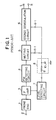
- FIG. 1 of the drawings A typical example of the FM receiving circuit is illustrated in Fig. 1 of the drawings and comprises a front end section 1 coupled to an antenna terminal 2, an intermediate frequency signal amplifier circuit 3, an FM detector circuit 4, a muting circuit 5, an FM demodulation circuit 6 associated with output terminals L and R, a level detecting circuit 7, and a low-pass filter circuit 8 provided with a resistor 9 and a capacitor 10.
- the FM receiving circuit When the FM receiving circuit is activated, FM signals are received and supplied from the antenna terminal 2 to the front end section 1.
- the front end section 1 is tuned in a selected frequency range, and, accordingly, the FM signal in the selected frequency range is extracted from the received broadcasting signals.
- the FM signal is converted into an intermediate frequency signal which is abbreviated as "IF signal”, and, then, the intermediate frequency signal is supplied to the intermediate frequency signal amplifier circuit 3.
- the output of the intermediate frequency signal amplifier circuit 3 is supplied to the FM detecting circuit 4 for demodulation into an FM composite signal.
- the intermediate frequency signal amplifier circuit 3 is provided with a plurality of amplifier circuits coupled in cascade, and the output signal of each amplifier circuits is detected by the level detecting circuit 7 provided in association therewith, then being summed again. Then, the level detecting circuit 7 produces a voltage signal which traces an envelope of the intermediate frequency signal. In other words, the voltage signal is representative of the electric field strength of the FM broadcasting signal received.
- the level detecting circuit 7 is further operative to rectify the intermediate frequency signal, and, for this reason, the audio signal is slightly demodulated. As a result, the voltage signal is varied in voltage level by not only the electric field strength of the FM broadcasting signal received but also the audio signal component.
- the muting circuit 5 starts on the muting operation when a control signal supplied to a control node 5-1 is decreased in voltage level below a predetermined level, and, for this reason, the FM composite signal is blocked by the muting circuit 5. THen, no FM composite signal is supplied to the stereo demodulation circuit 6.
- the stereo demodulation circuit 6 When the signal supplied to a control node 6-1 is decreased in voltage level below a predetermined level, the stereo demodulation circuit 6 is operative to gradually decrease the stereo separation factor between a right channel signal and a left channel signal by controlling the high cut off frequency. Thus, the stereo demodulation circuit 6 finally shifts the mode of operation from a stereophonic mode to a monaural mode. If the voltage signal produced by the level detecting circuit 7 is directly supplied to the control nodes 5-1 of the muting circuit 5 as the control signal, the voltage signal tends to deviate from the envelop of the intermediate frequency signal due to the audio signal component contained therein, which sometimes results in unintentional muting functions.
- the low pass filter circuit 8 is coupled between the level detecting circuit 7 and the control nodes 5-1 and 6-1.
- the low pass filter circuit 8 aims at elimination of the audio signal component from the voltage signal supplied from the level detecting circuit 7, thereby producing a voltage signal which is free from the audio signal component.
- the low pass filter circuit 8 is provided for allowing the voltage signal to vary substantially depending upon the electrical field strength only.
- the present invention proposes to change the time constant of the low-pass filter for quick response.
- an FM receiving circuit comprising a) a front end section operative to select an FM signal from FM broadcasting signals and producing an intermediate frequency signal on the basis of the FM signal, b) an audio signal producing section supplied with the intermediate frequency signal for producing audio signals and responsive to a first control signal for eliminating noise components due to a rapid variation in the electric field strength of the FM signal, c) a level detecting circuit supplied with an intermediate frequency signal transferred from the audio signal producing section and producing a voltage signal representative of an envelope of the intermediate frequency signal, d) a low-pass filter circuit providing a time constant for producing the first control signal on the basis of the voltage signal and responsive to a second control signal for variation in the time constant, e) a high-pass filter circuit operative to differentiate the voltage signal for producing a differential signal; and f) a rectifier circuit operative to rectify the differential signal for producing the second control signal.
- FIG. 2 of the drawings there is shown the circuit arrangement of an FM receiving circuit embodying the present invention.
- a front end section 1, an intermediate frequency signal amplifier circuit 3, an FM detecting circuit 4, a muting circuit 5, an FM demodulation circuit 6 and a level detecting circuit 7 are similar in circuit arrangement to those of the prior-art FM receiving circuit shown in Fig. 1, and, accordingly, no further description is hereinunder incorporated .
- the FM receiving circuit further comprises a low-pass filter circuit 18 with variable time constant for producing a first control signal on the basis of a voltage signal produced by the level detecting circuit 17.
- the low-pass filter circuit 18 is improved in accordance with the present invention and, accordingly, provided with a switch 30 and a bypassing node 27 together with the resistor 9 and the capacitor 10.
- the FM receiving circuit according to the present invention further comprises a high-pass filter circuit 19 for differentiating the voltage signal, a rectifying circuit 20, and a driving circuit 21.
- the low-pass filter circuit 18 is coupled at the input node 22 thereof to the level detecting circuit 17 and at the output node 23 to the muting circuit 15 and the FM demodulation circuit 16 in parallel manner.
- the low-pass filter circuit 18 further has a control node 24 where a second control signal is supplied from the driving circuit 21.
- the low-pass filter circuit 18 provides a time constant determined by the capacitance of the capacitor 10 and the resistance of the resistor 9, but the time constant is varied in the presence of the second control signal in such a manner as to couple the output node 23 to the bypassing node 27.
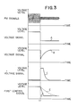
- the voltage signal produced by the level detecting circuit 7 is also decreased in voltage level as a waveform A.
- the voltage signal is supplied to not only the low-pass filter circuit 18 but also the high-pass filter circuit 19, and, accordingly, the high-pass filter circuit 19 tailors a waveform B for the output voltage signal thereof.
- the rectifier circuit 20 With the waveform B of the voltage signal, the rectifier circuit 20 produces a voltage signal having a waveform C which allows the driving circuit 21 to be activated.
- the switch 30 provides a conduction path between the bypassing node 27 and the output node 23, and, for this reason, the low-pass filter circuit 18 decreases the time constant thereof.
- the time constant is thus decreased in value, so that low-pass filter circuit 18 produces a waveform D for the first control signal which is rapidly lowered in voltage level in comparison with the waveform E produced by the low-pass filter incorporated in the prior-art FM receiving circuit.
- the muting circuit 15 and the FM demodulation circuit 16 quickly shift the mode of operation so as to cope with the unpleasant noises, thereby being improved in the response characteristics.
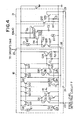
- Fig. 4 of the drawings the circuit arrangement of the essential part featuring the present invention is illustrated in detail.
- the essential part illustrated in Fig. 4 is constituted by a low pass filter circuit 18, a high pass filter circuit 19, a rectifying circuit 20 and a driving circuit 21, however the other arrangement is similar to that illustrated in Fig. 2, and, for this reason, no further description is hereinunder incorporated.
- a source of current I1 and bipolar transistors Q1 to Q3, Q8 to Q12, Q14 to Q16 and Q21 to Q23 form in combination a constant current biasing circuit, and bipolar transistors Q4 to Q7 and bipolar transistors Q17 to Q20 form input buffer circuits, respectively.
- Bipolar transistors Q24 and Q25 and a resistor R2 as a whole constitute an output buffer circuit, and a bipolar transistor Q13 serves as a switch.
- a source of current I3 and bipolar transistors Q27 and Q28 as a whole is operative to shift a dc biasing level, and resistors R5 and R6, bipolar transistors Q29 and Q30 and a source of current I2 form in combination a differential amplifier circuit which in turn forms the high-pass filter circuit 19 together with resistors R3 and R4 and a capacitor C2.
- a bipolar transistor Q31 serves as a rectifying circuit, and the emitter node and the base node thereof are coupled to the respective collector nodes of the bipolar transistors 29 and 30.
- the time constant determined by the resistor R3 and the capacitor C2 is selected in such a manner as to cope with a gradual variation of a voltage signal supplied to the node 28, and, for this reason, the bipolar transistor Q29 is substantially equal in collector voltage level to the bipolar transistor Q30 in an usual receiving condition, then the bipolar transistor Q31 remains in the off state.
- the node 28 is rapidly decreased in voltage level
- the base voltage level of the bipolar transistor Q29 follows the rapid decreasing, however, the capacitor C2 allows the bipolar transistor Q30 to keep the base voltage level. This results in that the bipolar transistor Q29 is higher in the collector voltage level than the bipolar transistor Q30. then, the bipolar transistor Q31 turns on.
- Bipolar transistors Q32 and Q33 and a resistor R7 as a whole constitute the driving circuit 21 and a node 29 is coupled to the control node 24 to propagate the second control signal.
- the capacitor C1 and the resistor R1 correspond to the capacitor 25 and the resistor 26, respectively.
- the bipolar transistors Q31 to Q33 remain off, so that no second control signal is supplied to the control node 24 of the low pass filter circuit 18. Then, the bipolar transistor Q13 turns on but the bipolar transistors Q14 to Q23 are turned off.
- the low-pass filter circuit 18 provides the time constant determined by the resistance of the resistor R1 and the capacitance of the capacitor C1, and the audio signal component is eliminated from the voltage signal supplied from the level detecting circuit 17, thereby allowing the first control signal to control the muting circuit 15 and the FM demodulation circuit 16 as similar to the prior-art FM receiving circuit.
- the voltage signal produced by the level detecting circuit 17 is also decreased in voltage level as a waveform A.
- the voltage signal is supplied to not only the low-pass filter circuit 18 but also the high-pass filter circuit 19, and, accordingly, the high-pass filter circuit 19 tailors a waveform B for a differential signal appearing at the collector node of the bipolar transistor Q29.
- the rectifier circuit 20 produces a waveform C at the base node of the bipolar transistor Q33, and, for this reason, the bipolar transistor Q33 turns on to cause the bipolar transistor Q13 to turn off.
- the circuitry formed by the bipolar transistors Q14 to Q23 is activated, and, accordingly, the low-pass filter circuit 18 varies the time constant to a value determined by the output impedance of the bipolar transistor Q20 of the emitter follower configuration and the capacitance of the capacitor C1.
- the time constant is thus decreased in value, so that low-pass filter circuit 18 produces a waveform D for the first control signal which is rapidly lowered in voltage level in comparison with the waveform E produced by the low-pass filter incorporated in the prior-art FM receiving circuit.
- the muting circuit 15 and the FM demodulation circuit 16 are improved in the response characteristics.
Landscapes
- Engineering & Computer Science (AREA)
- Computer Networks & Wireless Communication (AREA)
- Signal Processing (AREA)
- Noise Elimination (AREA)
- Circuits Of Receivers In General (AREA)
- Stereo-Broadcasting Methods (AREA)
Applications Claiming Priority (2)
| Application Number | Priority Date | Filing Date | Title |
|---|---|---|---|
| JP320691/87 | 1987-12-18 | ||
| JP62320691A JPH01162020A (ja) | 1987-12-18 | 1987-12-18 | Fmラジオ受信機 |
Publications (3)
| Publication Number | Publication Date |
|---|---|
| EP0320883A2 true EP0320883A2 (de) | 1989-06-21 |
| EP0320883A3 EP0320883A3 (en) | 1990-08-16 |
| EP0320883B1 EP0320883B1 (de) | 1994-04-13 |
Family
ID=18124264
Family Applications (1)
| Application Number | Title | Priority Date | Filing Date |
|---|---|---|---|
| EP88120820A Expired - Lifetime EP0320883B1 (de) | 1987-12-18 | 1988-12-13 | FM-Empfängerschaltung |
Country Status (5)
| Country | Link |
|---|---|
| US (1) | US4914715A (de) |
| EP (1) | EP0320883B1 (de) |
| JP (1) | JPH01162020A (de) |
| KR (1) | KR920001537B1 (de) |
| DE (1) | DE3889086T2 (de) |
Cited By (3)
| Publication number | Priority date | Publication date | Assignee | Title |
|---|---|---|---|---|
| DE4111709A1 (de) * | 1990-07-05 | 1992-01-16 | Pioneer Electronic Corp | Fm-tuner |
| WO1994022231A1 (de) * | 1993-03-24 | 1994-09-29 | Blaupunkt-Werke Gmbh | Rundfunkempfänger mit digitaler signalverarbeitung |
| EP0617519A3 (de) * | 1993-03-24 | 1995-01-25 | Blaupunkt Werke Gmbh | Schaltungsanordnung zur Ableitung mindestens eines von der Qualität eines empfangenen Signals abhängigen Qualitätssignals. |
Families Citing this family (18)
| Publication number | Priority date | Publication date | Assignee | Title |
|---|---|---|---|---|
| DE4027399C2 (de) * | 1990-08-30 | 1995-11-30 | Blaupunkt Werke Gmbh | UKW-Autoradio |
| US5113446A (en) * | 1990-12-17 | 1992-05-12 | Ford Motor Company | Stereo blend controller for FM receivers |
| DE59209341D1 (de) * | 1991-02-01 | 1998-07-02 | Blaupunkt Werke Gmbh | Verfahren zur Überbrückung von Audiosignalunterbrechungen |
| US5303405A (en) * | 1991-09-03 | 1994-04-12 | Motorola, Inc. | Comparator switched squelch rectifier |
| JP3018634B2 (ja) * | 1991-09-05 | 2000-03-13 | 日本電気株式会社 | Fm雑音低減回路 |
| JP3144574B2 (ja) * | 1991-11-20 | 2001-03-12 | ローム株式会社 | ミューティング制御回路 |
| US5303408A (en) * | 1992-04-03 | 1994-04-12 | Motorola, Inc. | Squelch detector |
| US6029053A (en) | 1995-09-12 | 2000-02-22 | Lockheed Martin Corp. | Apparatus and method for reducing co-channel radio interference |
| JPH0983388A (ja) * | 1995-09-19 | 1997-03-28 | Sony Corp | Fm受信機 |
| JP3599502B2 (ja) * | 1996-10-31 | 2004-12-08 | ミツミ電機株式会社 | Fm多重対応型ナビゲーション装置 |
| US6374124B1 (en) | 1997-12-24 | 2002-04-16 | Transcept, Inc. | Dynamic reallocation of transceivers used to interconnect wireless telephones to a broadband network |
| US6301240B1 (en) | 1998-02-19 | 2001-10-09 | Transcept, Inc. | Centrally located equipment for wireless telephone system |
| US6122529A (en) * | 1998-03-17 | 2000-09-19 | Transcept, Inc. | Simulcast with hierarchical cell structure overlay |
| JP2994362B1 (ja) | 1998-10-01 | 1999-12-27 | 三菱電機株式会社 | 高度道路交通システムの狭域通信用車載器 |
| DE69832078T2 (de) | 1998-11-30 | 2006-06-01 | Siemens Ag | Verfahren zur Rauschverminderung beim Empfang eines HF FM Signals |
| AU2003276579A1 (en) * | 2002-12-16 | 2004-07-09 | Koninklijke Philips Electronics N.V. | Noise suppression in an fm receiver |
| US8108044B2 (en) * | 2008-03-27 | 2012-01-31 | Medtronic, Inc. | Method and apparatus for the staged detection of RF energy |
| US8170515B2 (en) * | 2008-05-21 | 2012-05-01 | Medtronic, Inc. | Method and apparatus for the phased detection of a signal including a frequency deviation detection phase |
Family Cites Families (6)
| Publication number | Priority date | Publication date | Assignee | Title |
|---|---|---|---|---|
| US3628058A (en) * | 1970-02-24 | 1971-12-14 | Motorola Inc | Integrated dual time constant squelch circuit |
| US4087641A (en) * | 1976-04-01 | 1978-05-02 | Pioneer Electronic Corporation | Noise limiting circuit for FM stereo receiver |
| JPS5723332A (en) * | 1980-07-16 | 1982-02-06 | Clarion Co Ltd | Muting device |
| US4390749A (en) * | 1981-04-13 | 1983-06-28 | Superscope, Inc. | Noise control system for FM radio |
| JPS58164329A (ja) * | 1982-03-24 | 1983-09-29 | Mitsubishi Electric Corp | Fmミユ−テイング回路 |
| JPS59190748A (ja) * | 1983-04-13 | 1984-10-29 | Sharp Corp | Fm受信機のマルチパス歪軽減装置 |
-
1987
- 1987-12-18 JP JP62320691A patent/JPH01162020A/ja active Pending
-
1988
- 1988-12-12 US US07/283,182 patent/US4914715A/en not_active Expired - Fee Related
- 1988-12-13 DE DE3889086T patent/DE3889086T2/de not_active Expired - Fee Related
- 1988-12-13 EP EP88120820A patent/EP0320883B1/de not_active Expired - Lifetime
- 1988-12-16 KR KR1019880016759A patent/KR920001537B1/ko not_active Expired
Cited By (5)
| Publication number | Priority date | Publication date | Assignee | Title |
|---|---|---|---|---|
| DE4111709A1 (de) * | 1990-07-05 | 1992-01-16 | Pioneer Electronic Corp | Fm-tuner |
| WO1994022231A1 (de) * | 1993-03-24 | 1994-09-29 | Blaupunkt-Werke Gmbh | Rundfunkempfänger mit digitaler signalverarbeitung |
| EP0617519A3 (de) * | 1993-03-24 | 1995-01-25 | Blaupunkt Werke Gmbh | Schaltungsanordnung zur Ableitung mindestens eines von der Qualität eines empfangenen Signals abhängigen Qualitätssignals. |
| US5661809A (en) * | 1993-03-24 | 1997-08-26 | Blaupunkt-Werke Gmbh | Radio receiver having digital signal processing |
| US5673324A (en) * | 1993-03-24 | 1997-09-30 | Blaupunkt-Werke Gmbh | Radio receiver circuit for deriving at least one reception quality signal |
Also Published As
| Publication number | Publication date |
|---|---|
| KR920001537B1 (ko) | 1992-02-18 |
| EP0320883A3 (en) | 1990-08-16 |
| JPH01162020A (ja) | 1989-06-26 |
| DE3889086D1 (de) | 1994-05-19 |
| EP0320883B1 (de) | 1994-04-13 |
| US4914715A (en) | 1990-04-03 |
| KR890011281A (ko) | 1989-08-14 |
| DE3889086T2 (de) | 1994-07-28 |
Similar Documents
| Publication | Publication Date | Title |
|---|---|---|
| EP0320883B1 (de) | FM-Empfängerschaltung | |
| US4380824A (en) | Receiving reproducing system | |
| US4087641A (en) | Noise limiting circuit for FM stereo receiver | |
| US4146747A (en) | Fm stereo demodulating device | |
| US4628539A (en) | Muting circuit | |
| US4249137A (en) | Amplifier system with AGC, as for an AM radio | |
| US4313218A (en) | Extended AGC for a radio receiver | |
| US3714583A (en) | Muting circuit | |
| US2950356A (en) | Radio-phonograph circuits | |
| US4283793A (en) | Muting signal generation circuit for an FM receiver | |
| US5028883A (en) | Tone controller for attenuating noise in the signal generated by receiver from weak electric field, and receiver having the tone controller | |
| US4612662A (en) | Control circuit | |
| KR910004422B1 (ko) | 출력처리회로 | |
| US4710958A (en) | Circuit for controlling separation and high-cut operation of a stereo demodulator in an FM radio receiver | |
| EP0742642B1 (de) | Pegelregelungsschaltung für Empfänger | |
| JPS6046133A (ja) | ラジオ受信機 | |
| JPH04601Y2 (de) | ||
| JPS637710B2 (de) | ||
| US3559073A (en) | Forward agc circuit | |
| JPS6314505Y2 (de) | ||
| JP2723187B2 (ja) | 音声多重復調回路 | |
| JPS628976B2 (de) | ||
| JPS6013523B2 (ja) | 信号断続回路 | |
| JPS6223501B2 (de) | ||
| JPS6058637B2 (ja) | 自動飽和度制御回路 |
Legal Events
| Date | Code | Title | Description |
|---|---|---|---|
| PUAI | Public reference made under article 153(3) epc to a published international application that has entered the european phase |
Free format text: ORIGINAL CODE: 0009012 |
|
| 17P | Request for examination filed |
Effective date: 19881213 |
|
| AK | Designated contracting states |
Kind code of ref document: A2 Designated state(s): DE FR GB |
|
| PUAL | Search report despatched |
Free format text: ORIGINAL CODE: 0009013 |
|
| AK | Designated contracting states |
Kind code of ref document: A3 Designated state(s): DE FR GB |
|
| 17Q | First examination report despatched |
Effective date: 19930405 |
|
| GRAA | (expected) grant |
Free format text: ORIGINAL CODE: 0009210 |
|
| AK | Designated contracting states |
Kind code of ref document: B1 Designated state(s): DE FR GB |
|
| PG25 | Lapsed in a contracting state [announced via postgrant information from national office to epo] |
Ref country code: FR Effective date: 19940413 |
|
| REF | Corresponds to: |
Ref document number: 3889086 Country of ref document: DE Date of ref document: 19940519 |
|
| EN | Fr: translation not filed | ||
| PLBE | No opposition filed within time limit |
Free format text: ORIGINAL CODE: 0009261 |
|
| STAA | Information on the status of an ep patent application or granted ep patent |
Free format text: STATUS: NO OPPOSITION FILED WITHIN TIME LIMIT |
|
| 26N | No opposition filed | ||
| PGFP | Annual fee paid to national office [announced via postgrant information from national office to epo] |
Ref country code: GB Payment date: 20011212 Year of fee payment: 14 |
|
| REG | Reference to a national code |
Ref country code: GB Ref legal event code: IF02 |
|
| PGFP | Annual fee paid to national office [announced via postgrant information from national office to epo] |
Ref country code: DE Payment date: 20020109 Year of fee payment: 14 |
|
| PG25 | Lapsed in a contracting state [announced via postgrant information from national office to epo] |
Ref country code: GB Free format text: LAPSE BECAUSE OF NON-PAYMENT OF DUE FEES Effective date: 20021213 |
|
| PG25 | Lapsed in a contracting state [announced via postgrant information from national office to epo] |
Ref country code: DE Free format text: LAPSE BECAUSE OF NON-PAYMENT OF DUE FEES Effective date: 20030701 |
|
| GBPC | Gb: european patent ceased through non-payment of renewal fee |
Effective date: 20021213 |