EP0320918B1 - Procédé pour la réception d'une porteuse modulée par un signal utile - Google Patents
Procédé pour la réception d'une porteuse modulée par un signal utile Download PDFInfo
- Publication number
- EP0320918B1 EP0320918B1 EP88120923A EP88120923A EP0320918B1 EP 0320918 B1 EP0320918 B1 EP 0320918B1 EP 88120923 A EP88120923 A EP 88120923A EP 88120923 A EP88120923 A EP 88120923A EP 0320918 B1 EP0320918 B1 EP 0320918B1
- Authority
- EP
- European Patent Office
- Prior art keywords
- signal
- modulation
- phase
- histogram
- type
- Prior art date
- Legal status (The legal status is an assumption and is not a legal conclusion. Google has not performed a legal analysis and makes no representation as to the accuracy of the status listed.)
- Expired - Lifetime
Links
Images


Classifications
-
- H—ELECTRICITY
- H04—ELECTRIC COMMUNICATION TECHNIQUE
- H04L—TRANSMISSION OF DIGITAL INFORMATION, e.g. TELEGRAPHIC COMMUNICATION
- H04L27/00—Modulated-carrier systems
- H04L27/18—Phase-modulated carrier systems, i.e. using phase-shift keying
- H04L27/22—Demodulator circuits; Receiver circuits
- H04L27/227—Demodulator circuits; Receiver circuits using coherent demodulation
- H04L27/2271—Demodulator circuits; Receiver circuits using coherent demodulation wherein the carrier recovery circuit uses only the demodulated signals
- H04L27/2273—Demodulator circuits; Receiver circuits using coherent demodulation wherein the carrier recovery circuit uses only the demodulated signals associated with quadrature demodulation, e.g. Costas loop
-
- H—ELECTRICITY
- H04—ELECTRIC COMMUNICATION TECHNIQUE
- H04L—TRANSMISSION OF DIGITAL INFORMATION, e.g. TELEGRAPHIC COMMUNICATION
- H04L27/00—Modulated-carrier systems
- H04L27/0014—Carrier regulation
- H04L2027/0024—Carrier regulation at the receiver end
- H04L2027/0026—Correction of carrier offset
- H04L2027/0028—Correction of carrier offset at passband only
-
- H—ELECTRICITY
- H04—ELECTRIC COMMUNICATION TECHNIQUE
- H04L—TRANSMISSION OF DIGITAL INFORMATION, e.g. TELEGRAPHIC COMMUNICATION
- H04L27/00—Modulated-carrier systems
- H04L27/0014—Carrier regulation
- H04L2027/0024—Carrier regulation at the receiver end
- H04L2027/0026—Correction of carrier offset
- H04L2027/0038—Correction of carrier offset using an equaliser
Definitions
- the invention relates to a method for receiving signals in the form of carrier-signal-modulated carrier oscillations, in which the type of modulation used for an incoming signal is first determined with the aid of a histogram, and control information for adapting the circuit recovering the original signal to the determined type of modulation is produced therefrom .
- reference DE-A-34 14 969 discloses a radio reception device for Morse signals or telex signals that makes use of such a method, in which the incoming signal is first fed to a computing circuit, from which a histogram of signal frequencies plotted over time (histogram) is derived. created. This created histogram is then compared with sample histograms stored in a memory and the comparison is used to determine the type of modulation of the received signal. Following the determination of the type of modulation, the discriminator is adapted to this type of modulation and the received signal is fed to the discriminator.
- histogram histogram of signal frequencies plotted over time
- a universal transceiver is required for this, which can be adapted to the modem type of the remote station with regard to its modem.
- the invention is based on the problem of a method for automatic transmission of a universal transceiver designed for all types of DPSK permitted in the network Adapting the modem to the DPSK type of an incoming signal that is extremely reliable and requires only little additional equipment.
- the invention is based on the finding that it is very advantageous for the detection of the DPSK of an incoming signal to relate the frequency of values to a single quadrant and to evaluate the accumulation maxima that arise because this maximum evaluation can still be carried out perfectly even with a low signal-to-noise ratio .
- Fig. 1 shows a schematic representation of the transmission side of the modem of a transceiver.
- the digital useful information d (nT) for example with a bit rate of 2400 bit / sec, is converted into a signal pair, namely an in-phase signal I (nT / 2) and a quadrature signal Q (nT / 2), via a coding arrangement CAD. implemented with 1200 baud each.
- This pair of signals is fed to the modulator MOD, which consists of two mixers M1 and M2 on the input side.
- the mixers M1 and M2 are supplied with the carrier oscillation of 1800 Hz, for example, from a carrier generator TG at the second input, specifically to the mixer M1 and to the mixer M2 via a 90 ° phase-rotating element PH1.
- the phase modulation of the carrier oscillation carried out in the mixer M1 by the in-phase signal I (nT / 2) on the one hand, and the carrier oscillation phase-modulated in the mixer M2 by the quadrature signal Q (nT / 2) are converted via the adder AD to the outgoing signal s (pulse phase modulated) nTs) merged and this signal is transmitted in the baseband position or after conversion to a higher frequency position to the distant remote station.
- the outgoing signal s (nTs) modulated in the differential pulse phase has two or more different phase positions.
- FIGS. 2 and 3 are designed for the practically significant case of a 4 DPSK and a 16 DQAM.
- the coding arrangement CAD1 designed for a 4 DPSK according to FIG. 2 has on the input side a series parallel converter SP1, which issues the digital useful information d (nT) with the bit rate of 2400 bits / sec into two parallel bit streams, each with 1200 bits / sec, and that subsequent differential encoder DIC supplies.
- the differential encoder DIC supplies the signal pair already mentioned from the in-phase signal I (nT / 2) and the quadrature signal Q (nT / 2).
- the coding device CAD2 which is dimensioned for a 16 DQAM, also has a serial parallel converter SP2 on the input side, which divides the digital user information d (n2T) on the input side at a bit rate of 2400 bit / sec into four parallel bit streams, each with 600 bit / sec, and according to Fig. 2 feeds the differential encoder DIC.
- One pair of bits each at the output of the differential encoder DIC is fed to a digital-to-analog converter DA, and one of the digital-to-analog converters DA has the in-phase signal I (nT / 2) on the output side and the other digital-to-analog converter DA has the quadrature signal Q ( nT / 2).
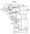
- the basic circuit diagram of the receiving side of the modem of a universal transceiver which makes use of the method for automatic adaptation to the DPSK type of the incoming signal s' (nTs), has an equalizer EZ on the input side, through which the incoming signal is passed to a demodulator DEM is fed.
- the demodulator DEM the signal pair consisting of the receiving-side in-phase signal I '(nT / 2) and the receiving-side quadrature signal Q' (nT / 2) is recovered from the incoming signal s' (nTs). For this, the incoming signal in turn fed to the first input of a mixer M1 and M2.
- the carrier oscillation of the clock generator TG is in turn present at the second input of the mixer M1 and at the second input of the mixer M2 via a 90 ° phase shifter PH1.
- the high-frequency components are suppressed on the mixer output side via low-pass filters TP and the signal pair thus received on the reception side is fed to the decoding arrangement DCA on the input side.
- the receiving-side in-phase signal I '(nT / 2) and the receiving-side quadrature signal Q' (nT / 2) at the output of the demodulator are also fed to the modulation type detection circuit MODE and a clock and carrier regeneration TR.
- the clock pulses TK supplied to the various circuit parts by the clock and carrier regeneration are only indicated by outgoing lines in FIG. 4.
- the modulation type detection circuit MODE has a converter UF1 on the input side, which converts the in-phase signal and the quadrature signal into a polar coordinate representation with the phase angle ⁇ and the amount A and then feeds the phase angle information and the amount information to the decision maker E1.
- This decision-maker E1 is followed by the actual histogram generator HG, which represents the clustering diagram required for the detection of the type of modulation and supplies the result to an evaluator AW for obtaining the control information necessary for setting the decoding arrangement DCA.
- the decoding arrangement DCA itself consists of a decision maker E and a decoder DC following the decision maker, at the output of which the transmitted original digital useful information d '(nT) or d' (n2T) can be taken.
- the correct setting of the input-side equalizer EC takes place as a function of the setting of the decision maker E of the decoding arrangement DCA.
- the more detailed details of the decision E1 according to FIG. 4 5 has a difference angle generator DB, to the input side of which the information relating to the phase angle ⁇ is fed directly at one input and at the other input via a delay element LG.
- the delay time of the delay element LG is one clock period.
- the differential phase angle ⁇ at the output of the differential angle generator DB is converted into the modulo 90 ° differential phase angle signal via the multiplier MZ and made available to the histogram generator HG.
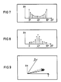
- FIG. 7 shows the characteristic course of the value frequency H for a 4 DPSK corresponding to V26 to A according to CCITT recommendation and FIG. 8 for a 4 over the difference phase angle ⁇ between 0 ° and 90 ° DPSK according to V26 to B according to CCITT recommendation.
- the decision maker E1 also has a converter UF2 to which the modulo 90 ° difference phase angle signal ⁇ ′ and the amount A are supplied on the input side.
- the converter UF2 in turn converts these signal values in polar coordinates into a Cartesian coordinate representation and makes them on the output side of the histogram generator HG according to FIG. 4 as a reformed in-phase signal I. ′ And quadrature signal Q 'Available for building a two-dimensional histogram.
- a detailed block diagram of a decoding arrangement DCA corresponding to FIG. 4 also shows FIG. 6.
- the input-side decision maker E here consists of an adjustable phase shifter PH2.
- the control input of this phase rotating element is supplied with a control signal st1 by the evaluator AW of the modulation type detection circuit MODE according to FIG. 4 as a function of the detected modulation type of the incoming signal s' (nTs).
- the decoder DC consists of the decoder DC1 for the phase angle and the decoder DC2 for the amplitude.
- the decoder DC2 is not required if the type of modulation 4 used for the incoming signal is DPSK, which has no amplitude modulation of the carrier oscillation.
- Both decoders DC1 and DC2 are connected in parallel to the output of the decision maker E.
- the decoder DC1 On the output side, the decoder DC1 has a parallel series converter PS1, which in turn combines the parallel bit streams at the two outputs of the decoder DC1 to form the signal representing the transmitted original digital useful information d '(nT).
- the output signal of the decision maker E is first limited in the decoder DC1 for the phase in the limiter BR to a constant amplitude value ⁇ K.
- the actual decoder DC1 for the phase is for the decoding of a 4 DPSK according to V26 to B.
- the CCITT recommendation measures and outputs the corresponding dibits at its two outputs to the parallel series converter PS1 in accordance with the occurring differential phases of 45 °, 135 °, 225 ° and 315 °.
- the modulation type detection circuit MODE detects a 4 DPSK corresponding to V26 to A according to the CCITT recommendation for the incoming signal, it outputs a control signal st1 to the phase setting element PH2, which signals the signals passing through the phase setting element PH2, namely the in-phase signal I ′ (nT) and the quadrature signal Q '(nT) rotates by + 45 °, thus converting the modulation types V26 to A into the modulation types V26 to B according to the CCITT recommendation for the decoder DC1.
- the modulation type detection circuit MODE outputs a control signal st2 to the output-side switch U of the decoding arrangement DCA, which switches the switch U into the switch position shown in the drawing.
- the decoder DC2 for the amplitude comes into play when not only the carrier phases but also the carrier amplitude is modulated for the incoming signal, as is the case with the 16 DQAM according to V22 up to the CCITT recommendation.
- the decoder DC2 has a quantizer QR on the input side, which is followed by a sub-bit decider SBE.
- the sub-bit decider SBE is followed by a bit adder BAD, to which, in addition to the two sub-bits containing the amplitude information, the bits representing the phase information are also fed from the output of the decoder DC1.
- the four parallel bits are then combined in the parallel-series converter PS2 in the transmitted user information d '(n2T) and output via the switch U to the output.
- the changeover switch U then contains a control signal st2 from the modulation type detection circuit which converts it into the switch position shown in broken lines.
- a buffer ZS may be provided in the signal path between the output of the demodulator DEM and the input of the decoding arrangement DCA, over which the receive-side in-phase signal I '(nT / 2) and quadrature signal Q' (nT / 2) are fed to the decoding arrangement DCA with a time delay in order to bridge this time interval.
- the method according to the invention can be used advantageously in transceivers for differential phase-modulated signals where, in networks with groups of transmitters and receivers that make use of different differential phase modulation, there is a requirement for individual subscribers by using a universal transceiver with each subscriber of the To be able to connect to the network.
Landscapes
- Engineering & Computer Science (AREA)
- Computer Networks & Wireless Communication (AREA)
- Signal Processing (AREA)
- Digital Transmission Methods That Use Modulated Carrier Waves (AREA)
Claims (4)
- Procédé de réception de signaux sous la forme de porteuses modulées par le signal utile, dans lequel le type de la modulation utilisée d'un signal d'entrée est tout d'abord déterminé à l'aide d'un histogramme, et de cela il découle une information de commande pour l'adaptation du circuit de récupération du signal d'origine, au type déterminé de la modulation,
caractérisé en ce que le signal d'entrée (s'(nTs)), dont la porteuse est modulée par le signal numérique utile (d(nt), d(n2T)), soit par l'utilisation, dans deux variantes possibles, d'une modulation différentielle de phase à quatre phases (4 DPSK), soit par l'utilisation d'une modulation différentielle de phase à seize phases (16 DQAM), est tout d'abord démodulé et ensuite le couple de signaux ainsi obtenu, à savoir le signal en phase (I'(nT)) et le signal en quadrature (Q'(nT)), d'une part, est envoyé à un dispositif de décodage (DCA) et, d'autre part, est représenté, après conversion en une représentation en coordonnées polaires donnant la phase (φ) et le module (A) et après formation de la différence de phase (Δ φ) entre des valeurs successives, dans un histogramme indiquant, dans un quadrant, la fréquence des valeurs (H), et que l'information de commande obtenue à l'aide de l'histogramme est envoyée au dispositif de décodage (DCA), sous la forme d'un signal de commande (st1), servant au réglage de phase, pour le dispositif de décision (E), et d'un signal de commande (st2) pour le décodeur (DC). - Procédé suivant la revendication 1,
caractérisé en ce que le couple de signaux (I'(nt), Q'(nT)), récupéré par démodulation à partir du signal d'entrée (s'(nTs)), est envoyé au dispositif de décodage (DCA) et par l'intermédiaire d'une mémoire temporaire (ZS), pendant une durée au moins égale au temps de détermination du type de la modulation et au temps de réglage du dispositif de décodage (DCA). - Procédé suivant la revendication 1 ou 2,
caractérisé en ce que la représentation de la fréquence des valeurs (H) de la différence phase (Δ φ) dans l'histogramme s'effectue modulo 90° et le type de la modulation est reconnu dans la zone de la différence de phase dans laquelle apparaît le maxima de la fréquence des valeurs. - Procédé suivant l'une des revendications précédentes,
caractérisé en ce que, pour reconnaître un signal d'entrée (s'(nTs)) à l'aide de la modulation 16 DQAM, on procède, au début, à une évaluation temporaire suivant ce que l'on désigne par "Trainingsmode" ("mode de conditionnement"), avec uniquement un couple de valeur déterminé et constitué de la différence de phase (Δ φ) et du module (A), par quadrant et pour la représentation d'un histogramme en deux dimensions rapporté à un quadrant.
Applications Claiming Priority (2)
| Application Number | Priority Date | Filing Date | Title |
|---|---|---|---|
| DE3742865 | 1987-12-17 | ||
| DE3742865 | 1987-12-17 |
Publications (3)
| Publication Number | Publication Date |
|---|---|
| EP0320918A2 EP0320918A2 (fr) | 1989-06-21 |
| EP0320918A3 EP0320918A3 (en) | 1990-12-19 |
| EP0320918B1 true EP0320918B1 (fr) | 1993-11-03 |
Family
ID=6342874
Family Applications (1)
| Application Number | Title | Priority Date | Filing Date |
|---|---|---|---|
| EP88120923A Expired - Lifetime EP0320918B1 (fr) | 1987-12-17 | 1988-12-14 | Procédé pour la réception d'une porteuse modulée par un signal utile |
Country Status (4)
| Country | Link |
|---|---|
| US (1) | US4933958A (fr) |
| EP (1) | EP0320918B1 (fr) |
| DE (1) | DE3885426D1 (fr) |
| ZA (1) | ZA889399B (fr) |
Families Citing this family (11)
| Publication number | Priority date | Publication date | Assignee | Title |
|---|---|---|---|---|
| JP2748536B2 (ja) * | 1989-04-25 | 1998-05-06 | 日本電気株式会社 | 直交信号復調装置 |
| US5553098A (en) * | 1994-04-12 | 1996-09-03 | Sicom, Inc. | Demodulator with selectable coherent and differential data |
| US5687163A (en) * | 1995-06-07 | 1997-11-11 | Cirrus Logic, Inc. | Method and apparatus for signal classification using I/Q quadrant histogram |
| US5914990A (en) * | 1995-11-22 | 1999-06-22 | Telefonaktiebolaget Lm Ericsson | Filtering in a receiver that uses log-polar signal processing |
| US6463107B1 (en) | 1999-07-01 | 2002-10-08 | Telefonaktiebolaget Lm Ericsson (Publ) | Methods and apparatuses for synchronization and modulation type detection |
| US20010055348A1 (en) * | 2000-03-31 | 2001-12-27 | Anderson Christopher L. | Sequential quadrant demodulation of digitally modulated radio signals |
| US7469022B2 (en) * | 2004-11-23 | 2008-12-23 | Via Technologies, Inc. | Methods and apparatus for symmetrical phase-shift keying |
| US7610110B1 (en) * | 2006-06-02 | 2009-10-27 | Adobe Systems Incorporated | Graphically displaying stereo phase information |
| GB2439125A (en) * | 2006-06-13 | 2007-12-19 | Siconnect Ltd | DQPSK timing estimation using quaternary to polar conversion |
| WO2009095024A2 (fr) * | 2008-01-31 | 2009-08-06 | Coloplast A/S | Matériaux textiles à adhésif et leurs procédés d'utilisation |
| US12250100B2 (en) * | 2022-02-14 | 2025-03-11 | David E. Newman | Selecting a modulation scheme responsive to fault types in 5G/6G |
Family Cites Families (7)
| Publication number | Priority date | Publication date | Assignee | Title |
|---|---|---|---|---|
| FI53904C (fi) * | 1972-03-17 | 1978-08-10 | Nokia Oy Ab | Foerfarande foer demodulering av en differentialt fasmodulerad signal |
| DE2752468A1 (de) * | 1977-11-24 | 1979-05-31 | Ferdinand Dipl Ing Liedtke | Verfahren zur automatischen erkennung phasengetasteter signale mit unbekannten parametern |
| GB2106734B (en) * | 1981-09-15 | 1986-01-15 | Standard Telephones Cables Ltd | Radio receiver |
| DE3414969C2 (de) * | 1983-04-27 | 1986-05-15 | Siemens AG, 1000 Berlin und 8000 München | Funkempfangseinrichtung |
| US4546322A (en) * | 1983-08-24 | 1985-10-08 | Reliance Electric Company | Adaptable demodulator for arbitrary amplitude and phase keyed modulation signals |
| US4731796A (en) * | 1984-10-25 | 1988-03-15 | Stc, Plc | Multi-mode radio transceiver |
| FR2595895B1 (fr) * | 1986-03-13 | 1988-05-13 | France Etat | Double demodulateur numerique |
-
1988
- 1988-12-07 US US07/280,817 patent/US4933958A/en not_active Expired - Fee Related
- 1988-12-14 DE DE88120923T patent/DE3885426D1/de not_active Expired - Fee Related
- 1988-12-14 EP EP88120923A patent/EP0320918B1/fr not_active Expired - Lifetime
- 1988-12-15 ZA ZA889399A patent/ZA889399B/xx unknown
Also Published As
| Publication number | Publication date |
|---|---|
| EP0320918A2 (fr) | 1989-06-21 |
| EP0320918A3 (en) | 1990-12-19 |
| DE3885426D1 (de) | 1993-12-09 |
| ZA889399B (en) | 1989-08-30 |
| US4933958A (en) | 1990-06-12 |
Similar Documents
| Publication | Publication Date | Title |
|---|---|---|
| DE69515312T2 (de) | Direktmischempfänger | |
| DE2244690C3 (de) | Einrichtung zur Zweiseitenband-Quadraturmodulation | |
| DE4191766C2 (de) | Frequenzsteuerschaltkreis für einen einstellbaren Empfänger-Oszillator | |
| DE3223408C2 (fr) | ||
| DE69427024T2 (de) | Digitales vermittlungssystem und empfänger zur verwendung darin | |
| EP0320918B1 (fr) | Procédé pour la réception d'une porteuse modulée par un signal utile | |
| DE68918010T2 (de) | Kodiertes Modulationsübertragungssystem. | |
| DE69826415T2 (de) | Einseitenbandübertragung von QPSK-, QAM- und sonstigen Signalen | |
| DE69030402T2 (de) | System zur Unterbrechung der Ausgangswellen eines Senders | |
| DE2817338A1 (de) | Uebertragungsgeschwindigkeits-waehlsystem | |
| DE69330554T2 (de) | Asynchrones modem für variable geschwindigkeiten | |
| DE69834631T2 (de) | Netzwerk zur symboltaktrückgewinnung für ein trägenloses amplituden-phasen (cap) signal | |
| DE102004052898B4 (de) | Kompensation des Trägerfrequenz-Offsets in einer für mehrere Modulationsarten ausgelegten Empfangsvorrichtung eines mobilen Kommunikationssystems | |
| DE10318643B4 (de) | Mehrwertiges FSK Frequenzmodulationssystem | |
| DE2944235C2 (fr) | ||
| DE69829661T2 (de) | Weichentscheidungsverfahren und-vorrichtung bei einer 8-PSK-Demodulation | |
| EP0080020B1 (fr) | Procédé pour la détermination des instants d'échantillonnage d'un signal reçu en modulation de quadrature de phase manipulée ou en modulation de quadrature d'amplitude | |
| DE69422178T2 (de) | Verfahren zur demodulation von digital modulierten signalen und demodulator | |
| EP0254846A1 (fr) | Procédé et dispositif de transmission de données | |
| DE3750324T2 (de) | Vereinfachte Zurückgewinnung von Daten aus Signalen mit Quadraturträgern. | |
| EP1556986B1 (fr) | Procede et circuit pour generer un symbole auxiliaire pour le reglage d'un demodulateur maq | |
| DE3787994T2 (de) | Kommunikationssystem, Empfänger und Sender und Methode zur Datenrückgewinnung. | |
| DE3243373C2 (fr) | ||
| DE3015218C2 (fr) | ||
| DE69128975T2 (de) | Trägerrückgewinnungsverfahren für Modulation mit grosser Anzahl Phasen- und Amplitudenzustände |
Legal Events
| Date | Code | Title | Description |
|---|---|---|---|
| PUAI | Public reference made under article 153(3) epc to a published international application that has entered the european phase |
Free format text: ORIGINAL CODE: 0009012 |
|
| AK | Designated contracting states |
Kind code of ref document: A2 Designated state(s): CH DE GB LI NL |
|
| PUAL | Search report despatched |
Free format text: ORIGINAL CODE: 0009013 |
|
| AK | Designated contracting states |
Kind code of ref document: A3 Designated state(s): CH DE GB LI NL |
|
| 17P | Request for examination filed |
Effective date: 19901126 |
|
| 17Q | First examination report despatched |
Effective date: 19930326 |
|
| GRAA | (expected) grant |
Free format text: ORIGINAL CODE: 0009210 |
|
| AK | Designated contracting states |
Kind code of ref document: B1 Designated state(s): CH DE GB LI NL |
|
| REF | Corresponds to: |
Ref document number: 3885426 Country of ref document: DE Date of ref document: 19931209 |
|
| PG25 | Lapsed in a contracting state [announced via postgrant information from national office to epo] |
Ref country code: LI Effective date: 19931231 Ref country code: CH Effective date: 19931231 |
|
| GBT | Gb: translation of ep patent filed (gb section 77(6)(a)/1977) |
Effective date: 19940111 |
|
| REG | Reference to a national code |
Ref country code: CH Ref legal event code: PL |
|
| PLBE | No opposition filed within time limit |
Free format text: ORIGINAL CODE: 0009261 |
|
| STAA | Information on the status of an ep patent application or granted ep patent |
Free format text: STATUS: NO OPPOSITION FILED WITHIN TIME LIMIT |
|
| 26N | No opposition filed | ||
| PGFP | Annual fee paid to national office [announced via postgrant information from national office to epo] |
Ref country code: DE Payment date: 19950217 Year of fee payment: 7 |
|
| PGFP | Annual fee paid to national office [announced via postgrant information from national office to epo] |
Ref country code: GB Payment date: 19951123 Year of fee payment: 8 |
|
| PGFP | Annual fee paid to national office [announced via postgrant information from national office to epo] |
Ref country code: NL Payment date: 19951230 Year of fee payment: 8 |
|
| PG25 | Lapsed in a contracting state [announced via postgrant information from national office to epo] |
Ref country code: DE Effective date: 19960903 |
|
| PG25 | Lapsed in a contracting state [announced via postgrant information from national office to epo] |
Ref country code: GB Effective date: 19961214 |
|
| PG25 | Lapsed in a contracting state [announced via postgrant information from national office to epo] |
Ref country code: NL Effective date: 19970701 |
|
| GBPC | Gb: european patent ceased through non-payment of renewal fee |
Effective date: 19961214 |
|
| NLV4 | Nl: lapsed or anulled due to non-payment of the annual fee |
Effective date: 19970701 |