EP0321028A2 - Emitter-coupled logic circuit with three-state capability - Google Patents
Emitter-coupled logic circuit with three-state capability Download PDFInfo
- Publication number
- EP0321028A2 EP0321028A2 EP88202821A EP88202821A EP0321028A2 EP 0321028 A2 EP0321028 A2 EP 0321028A2 EP 88202821 A EP88202821 A EP 88202821A EP 88202821 A EP88202821 A EP 88202821A EP 0321028 A2 EP0321028 A2 EP 0321028A2
- Authority
- EP
- European Patent Office
- Prior art keywords
- voltage
- transistor
- circuit
- resistor
- coupled
- Prior art date
- Legal status (The legal status is an assumption and is not a legal conclusion. Google has not performed a legal analysis and makes no representation as to the accuracy of the status listed.)
- Ceased
Links
- QHPJWPQRZMBKTG-UHFFFAOYSA-N ethyl 2-[2-methoxy-4-[(4-oxo-2-sulfanylidene-1,3-thiazolidin-5-ylidene)methyl]phenoxy]acetate Chemical compound C1=C(OC)C(OCC(=O)OCC)=CC=C1C=C1C(=O)NC(=S)S1 QHPJWPQRZMBKTG-UHFFFAOYSA-N 0.000 claims description 10
- 230000000295 complement effect Effects 0.000 claims description 5
- 239000000543 intermediate Substances 0.000 claims 4
- 230000005540 biological transmission Effects 0.000 claims 2
- 230000001747 exhibiting effect Effects 0.000 claims 1
- 230000004044 response Effects 0.000 description 7
- 238000010586 diagram Methods 0.000 description 4
- 239000002131 composite material Substances 0.000 description 1
- 238000007599 discharging Methods 0.000 description 1
- 230000005669 field effect Effects 0.000 description 1
- 230000003993 interaction Effects 0.000 description 1
- 238000000034 method Methods 0.000 description 1
- 238000012986 modification Methods 0.000 description 1
- 230000004048 modification Effects 0.000 description 1
- 230000008569 process Effects 0.000 description 1
- 239000004065 semiconductor Substances 0.000 description 1
Images


Classifications
-
- H—ELECTRICITY
- H03—ELECTRONIC CIRCUITRY
- H03K—PULSE TECHNIQUE
- H03K17/00—Electronic switching or gating, i.e. not by contact-making and –breaking
- H03K17/51—Electronic switching or gating, i.e. not by contact-making and –breaking characterised by the components used
- H03K17/56—Electronic switching or gating, i.e. not by contact-making and –breaking characterised by the components used by the use, as active elements, of semiconductor devices
- H03K17/60—Electronic switching or gating, i.e. not by contact-making and –breaking characterised by the components used by the use, as active elements, of semiconductor devices the devices being bipolar transistors
- H03K17/603—Electronic switching or gating, i.e. not by contact-making and –breaking characterised by the components used by the use, as active elements, of semiconductor devices the devices being bipolar transistors with coupled emitters
-
- H—ELECTRICITY
- H03—ELECTRONIC CIRCUITRY
- H03K—PULSE TECHNIQUE
- H03K19/00—Logic circuits, i.e. having at least two inputs acting on one output; Inverting circuits
- H03K19/02—Logic circuits, i.e. having at least two inputs acting on one output; Inverting circuits using specified components
- H03K19/08—Logic circuits, i.e. having at least two inputs acting on one output; Inverting circuits using specified components using semiconductor devices
- H03K19/082—Logic circuits, i.e. having at least two inputs acting on one output; Inverting circuits using specified components using semiconductor devices using bipolar transistors
- H03K19/0823—Multistate logic
- H03K19/0826—Multistate logic one of the states being the high impedance or floating state
-
- H—ELECTRICITY
- H03—ELECTRONIC CIRCUITRY
- H03K—PULSE TECHNIQUE
- H03K19/00—Logic circuits, i.e. having at least two inputs acting on one output; Inverting circuits
- H03K19/02—Logic circuits, i.e. having at least two inputs acting on one output; Inverting circuits using specified components
- H03K19/08—Logic circuits, i.e. having at least two inputs acting on one output; Inverting circuits using specified components using semiconductor devices
- H03K19/082—Logic circuits, i.e. having at least two inputs acting on one output; Inverting circuits using specified components using semiconductor devices using bipolar transistors
- H03K19/086—Emitter coupled logic
Definitions
- This invention relates generally to electronic circuits using emitter-coupled logic (ECL) and, in particular, to an ECL circuit capable of operating in the three-state mode.
- ECL emitter-coupled logic
- three-state refers to a specific operational mode in which the digital circuit is electronically disconnected from the further circuitry without being physically disconnected from it. More precisely, the digital circuit has an output terminal from which information is supplied to an input point of the further circuitry. While continuing to accept and process input data, the digital circuit can be switched from (a) condition in which the output terminal exhibits low impedance to the further circuitry as the digital circuit switches between a pair of binary logic states to (b) a condition in which the output terminal exhibits very high impedance to the further circuitry. The latter condition is the third state. Due to the high output impedance, the input point of the further circuitry is effectively disconnected from the output terminal.
- Three-state is highly advantageous when the further circuitry is driven by a number of digital circuits, only one of which provides information intended to drive the further circuitry at any given time. By placing the other circuits in the three-state mode, they do not load the further circuitry. This allows it to operate more efficiently. Use of three-state also avoids undesirable interactions among the digital circuits by way of the further circuitry.
- FIG. 1 shows a prior art system containing M three-state logic circuits 101 - 10 M , of which at least circuit 101 is a TTL gate. Circuits 101 - 10 M provide a one-bit data bus 12 with digital information in response to digital input signals V I1 - V IM and output enabling signals V OE1 - V OEM . Data bus 12 is terminated by resistors R TC and R TE to respective sources of high and low supply voltages V CC and V EE .
- the V OE signals for all but one of circuits 101 - 10 M are normally at output disabling values that place those M-1 circuits in the three-state mode to electrically disconnect their output terminals from bus 12.
- the V OE signal for the remaining one of circuits 101 - 10 M is at an output enabling value. This enables bus 12 to accept its output signal.
- circuit 101 it consists of (1) a TTL input stage 14, (b) a TTL output stage 16 formed with NPN transistors QA, QB, QC, and QD and resistors RA, RB, RC, and RD, and (c) a three-state switching stage 18 formed with a control circuit 20 and an NPN transistor QE.
- Gate 101 provides its output signal at an output terminal T O connected to bus 12.
- signal V OE1 is at the output enabling value
- control 20 maintains transistor QE in the off condition to prevent it from affecting output stage 16.
- one of output transistors QC and QD is on while the other is off. his defines two logic states. In both cases, current flows through terminal T O , so that it exhibits low output impedance.
- Control 20 turns transistor QE on when signal V OE1 is switched to the output disabling value. This causes transistors QA and QB to turn off regardless of their prior conductive conditions which, in turn, similarly causes both of output transistors QC and QD to turn off. Circuit 101 goes into the three-state mode. Substantially no current flows through terminal T O . It now presents a very high output impedance. The presence of two serially connected output transistors make TTL very conductive to three-state.
- FIG. 2a illustrates how a conventional ECL output stage 22 interfaces with a one-bit data bus 24.
- Stage 22 centers around main NPN transistors Q1 A and Q1 B whose bases respectively receive base input signals V A and V B .
- the emitters of transistors Q1 A and Q1 B are connected together at a node N1 in a differential configuration. Their collectors are respectively coupled through small equal-size load resistors R1 A and R1 B to the V CC supply.
- a main current source 26 connected between node N1 and the V EE supply provides a main supply current I M for transistors Q1 A and Q1 B .
- An intermediate voltage signal V ITM representative of the state of stage 22 is taken from a node N2 at the Q1 A collector.
- V ITM is supplied to the base of an NPN output transistor Q2 whose collector is tied to the V CC supply. Transistor Q2 is always on during circuit operation. Stage 22 provides its output signal to bus 24 by way of terminal T O connected to the Q2 emitter. The signal voltage on bus 24 is thus about 1V BE and V ITM .
- V BE is the standard voltage of 0.7 - 0.8 volt that exists across the base-emitter junction of a bipolar transistor when it just reaches full conduction in the forward direction.
- Bus 24 is terminated by a resistor R T to a source of a termination voltage V TT which is usually about 2 volts below V CC .
- Stage 22 is at a high binary stage (or logical"1") when transistor Q1 A is off and transistor Q1 B is on. This usually arises when the voltage difference V B - V A is about 100 millivolts. None of supply current I M flows through resistor R1 A . The only current flowing through resistor R1 A is the small current needed to drive the Q2 base. As a result, voltage V ITM is at a high level near V CC . Because transis tor Q2 is on, current flows through terminal T O causing it to exhibit a low impedance to bus 24.
- Stage 22 goes into a low binary state (or logical "O") when V B - V A is reversed so as to turn transistor Q1 A on and turn transistor Q1 B off. All of current I M flows through resistor R1 A . Voltage V ITM drops to a low level approximately equal to V CC - I M R1, where R1 is the resistance of resistor R1 A or R1 B . The voltage swing I N R1 is typically in the neighborhood of 1V BE . Terminal T O exhibits a low impedance to bus 24. Stage 22 thus switches between two binary logic states, both at low output impedance.
- This Signetics 100123 ECL integrated circuit is a bus driver of the type employed in Gustafson et al. With reference to Fig. 2a, voltage swing I M R1 is raised to double its normal value in output stage 22 of the Signetics 100123. This enables transistor Q2 to turn off when stage 22 is in the low (but not the high) logic state. Terminal T O presents a high impedance to bus 24 during that time. Even though the Signetics 100123 still operates in only two different states, it does achieve some of the advantages of three-state. However, the increased voltage and the charging/discharging of the Q2 base during normal switching cause the Signetics 100123 to operate significantly slower than an otherwise comparable ECL device.
- FIG. 2b illustrates an ECL output stage 28 having a wired-OR capability.
- Stage 28 is the same as stage 22 depicted in Fig. 2a except that an NPN transistor Q1 C is connected between node N1 and the Q1 B collector.
- a control voltage V C is supplied to the Q1 C base.
- Transistor Q1 C turns on when V C is raised to a suitable high value. All of current I M flows through resistor R1 B . V ITM thereby goes to its high level irrespective of the values of V A and V B . Alternatively, the Q1 B collector could be connected to the Q1 A collector. V ITM would then go unilaterally to its low level.
- the wired-OR arrangement comes close to three-state in the sense that stage 28 can be placed at either a high logic state or a low logic state regardless of the values of V A and V B . However, wired-OR does not provide a true three-state capability in which there are two binary states at low output impedance and one state at high output impedance.
- ECL operates much faster than TTL. Accordingly, it would be highly desirable to have an ECL circuit that can be operated in the three-state mode over the normal ECL output voltage range extending from V CC - 2 volts to V CC .
- the present invention is logic circuit that provides such a capability.
- the core of this circuit consists of first and second like-polarity bipolar transistors arranged in a differential configuration.
- the first transistor has a base that receives an input voltage, an emitter coupled to a first node, and a collector coupled to a second node at which an intermediate voltage signal representative of the state of the circuit is provided.
- the second transistor has a base that receives another input voltage, an emitter coupled to the first node, and a collector coupled to a source of a first supply voltage.
- a current source coupled between the first node and a source of a second supply voltage provides a main supply current at the first node.
- a resistor is coupled between the second node and the source of the first supply voltage.
- the intermediate signal is at a first voltage level representing a first logic state when the first transistor is off and the second transistor is on so that largely none of the main supply current flows through the resistor.
- the intermediate signal is at a second voltage level representing a second logic state when the first transistor is on and the second transistor is off so that largely all of the main supply current flows through the resistor.
- the second voltage level is closer to the second supply voltage than the first voltage level.
- the circuit contains a like-polarity bipolar output transistor having a base coupled to the second node, an emitter coupled to an output terminal, and a collector coupled to a voltage source.
- the output transistor is turned on when the intermediate signal is at the first or second voltage level.
- the output terminal thereby exhibits low impedance to further circuitry driven from the output terminal.
- a switching stage controls the intermediate signal in response to that output control signal.
- the switching stage causes current exceeding the main supply current to flow through the resistor irrespective of the conductive conditions of the first and second transistors. Consequently, the intermediate signal reaches a voltage closer to the second supply voltage than the second level. This places the circuit in a third state.
- the further circuitry prevents the voltage at the output terminal from getting any closer to the second supply voltage than a termination voltage that lies between the supply voltages.
- the termination voltage is sufficiently close to the first supply voltage that the output transistor turns off when the control signal reaches the specified condition.
- the output terminal then exhibits very high impedance to the further circuitry, effectively disconnecting it from the logic circuit. In this way, the present ECL circuit achieves a true three-state capability over the portion of the supply voltage range extending between the first supply voltage and the termination voltage.
- FIG. 3 it illustrates an example of a system capable of achieving three-state with ECL.
- This system is formed with M three-state logic circuits 301 - 30 M , of which at least circuit 301 is an ECL gate.
- Circuits 301 - 30 M operate as a group in response to digital input signals V I1 and V IM and output enabling signals V OE1 and V OEM to control the information transmitted on a one-bit data bus 32 in the same way that circuits 101 - 10 M in Fig. 1 control the data transmitted on bus 12.
- Bus 32 is preferably terminated at both ends through equal valve resistors R T1 and R T2 to the V TT termination supply.
- bus 32 could be arranged as shown in Fig. 2a or 2b for bus 24. In either case, termination voltage VT T lies between supply voltages V CC and V EE .
- ECL circuit 301 consists of an input stage 34, an output stage 36, and a three-state switching stage 38.
- Output stage 36 is a good starting point for examining the configuration and operation of gate 301.
- Output stage 36 is a differential amplifier containing main NPN transistors Q1 A and Q1 B , load resistors R1 A and R1 B , current source 26, and NPN output transistor Q2 all arranged as in Fig. 2a.
- Resistor R1 A is essential to the circuit design because the voltages defining the states of circuit 301 are produced across it.
- V CC - V TT - V BE must be greater than the voltage swing I M R1 across resistor R1 A .
- resistor R1 B is employed basically to provide "balancing" for a temperature compensation circuit 40 connected between the Q1 A and Q1 B collectors. Compensation circuit 40 stabilizes the circuit output signal against temperature variations.
- a voltage clamp 42 A is connected between the V CC supply and the Q1 A collector (or node N2). Clamp 42 A prevents the voltage across resistor R1 A from exceeding a clamped value V CL . For reasons dealt with below, V CL is greater than V CC - V TT - V BE .
- Another voltage clamp 42 B connected between the V CC supply and the Q1 B collector prevents the voltage across resistor R1 B from exceeding V CL . Clamp 42 B rarely becomes active. It basically "balances" clamp 42 A to allow circuit 40 to operate efficiently.
- stage 36 When signal V OE1 is at the output enabling value, stage 36 operates in the manner described above for stage 22 in Fig. 2a. Clamps 42 A and 42 B are inactive since V CL is greater than I M R1. When transistor Q1 A is off and transistor Q1 B is on so that largely none of supply current I M flows through resistor R1 A , intermediate voltage V ITM reaches a high level near V CC representing the high binary state. V ITM drops to a low value approximately equal to V CC - I M R1 representing the low binary state when transistor Q1 A is on and transistor Q1 B is off so that largely none of current I M flows through resistor R1 A .
- Transistor 22 is turned on during the times that V ITM switches between V CC and V CC - I M R1.
- terminal T O exhibits low impedance to bus 32.
- input stage 34 it consists of an ECL input circuit 44 and a level-shifting circuit 46.
- input circuit 44 In response to input signal V I1 , input circuit 44 generates complentary input voltages V HA and V HB that vary from a low value V HMIN lying between V CC and V EE to a high value near V CC .
- V HMIN is usually about 1V BE below V CC .
- Level-shifting circuit 46 produces base input voltages V A and V B by respectively shifting voltages V HA and V HB downward by an amount equal to 1V BE plus an additional level shift V LS . Consequently, voltages V A and V B are complementary signals that vary from V HMIN - V BE - V LS approximately to V CC - V BE - V LS .
- Circuit 46 is divided into two identical sections.
- One of the sections is formed with an NPN level-shift transistor Q3 A that provides a downshift equal to 1V BE , a level-shift element 48 A that provides a downshift equal to V LS , and a current source 50 A connected between a node N3 A and the V EE supply.
- the other section is similarly formed with an NPN level-shift transistor Q3 B that provides a 1V BE downshift, a level-shift element 48 B that provides a V LS downshift, and a current source 50 B connected between a node N3 B and the V EE supply.
- Voltages V HA and V HB are respectively supplied to the bases of transistors Q3 A and Q3 B whose collectors are tied to the V CC supply.
- Level-shift elements 48 A and 48 B are respectively connected between the emitters of transistors Q3 A and Q3 B and nodes N3 A and N3 B from which voltages V A and V B are taken.
- Level shifts 48 A and 48 B operate in conjunction with clamp 42 A to prevent transistor Q1 A from going into deep saturation when signal V OE1 is at the output disabling value -- i.e., gate 301 is in the three-state mode. This avoids a loss in response time that might otherwise occur when V OE1 is switched to the output enabling value to remove circuit 301 from the three-state mode.
- V LS satisfies the relationship V LS > V CL - V BE - V SV (1) where V SV is the maximum tolerable forward voltage from the base of transistor Q1 A to its collector. Since transistor Q1 A goes into deep saturation when its base-to-collector voltage reaches 1V BE , V SV is somewhat less than 1V BE . S SV is usually no more than 0.5 volt and is preferably close to 0 volt. Good operation occurs when V LS equals V CL - V BE . Level shifts 48 A and 48 B similarly operate in combination with clamp 42 B to prevent transistor Q1 B from going into deep saturation.
- Switching circuit 38 consists of a control circuit 52 and a differential amplifier 54.
- Control circuit 52 produces complementary flow-control voltages V D and D E in response to signal V OE1 .
- Differential amplifier 54 is formed with flow transistors Q4 D and Q4 E and a current source 56 connected between the V EE supply and a node N4. Voltages V D and V E are respectively supplied to the control electrodes of transistors Q4 D and Q4 E which have first flow electrodes connected to node N4 to receive a further supply current I F from current source 56.
- Transistor Q4 D has a second flow electrode connected to node N2.
- Transistor Q4 E has a second flow electrode tied to the V CC supply.
- Transistors Q4 D and Q4 E are preferably NPN transistors as indicated in Fig. 3. The first, second, and control electrodes of each transistor Q4 D or Q4 E are then respectively its emitter, collector, and base. Alternatively transistors Q4 D and Q4 E might be N-channel field-effect transistors of the insulated-gate or junction type. In this case, the source, drain, and gate electrode are respectively the first, second, and control electrodes of each transistor Q4 D or Q4 E .
- Switching circuit 38 operates in the following way.
- control circuit 52 produces voltages V E and V D at respective high and low values.
- Transistor Q4 E is turned on.
- Transistor Q4 D is turned off to prevent circuit 38 from affecting the operation of output stage 36.
- Control 52 reverses the values of V D and V E when V OE1 is switched to the output disabling value.
- Transistor Q4 E turns off.
- Transistor Q4 D turns on and draws at least part of further supply current I F through resistor R1 A .
- the circuit parameters are chosen in such a way that current greater than main supply current I M flows through resistor R1 A regardless of the conditions of transistors Q1 A and Q1 B .
- Signal V ITM drops to a voltage below V CC - I M R1. This places circuit 301 in a third state.
- transistor Q2 For gate 301 to be electrically disconnected from bus 32, transistor Q2 must turn off irrespective of the condition of bus 32 and irrespective of the conductive conditions of transistors Q1 A and Q1 B .
- the "worst case" arises when transistor Q1 A is off and the bus voltage equals V TT . This is the situation in which the current that transistor Q4 D draws through resistor R1 A in order to force V ITM to a voltage low enough to turn off transistor Q2 is at its maximum value I FR .
- Clamp 42 A may be active or inactive in the "worst case". If clamp 42 A is active, it draws part of current I F . Consequently, I F is greater than I FR . If clamp 42 A is inactive, I F approximately equals I FR .
- Transistor Q2 turns off when its base-to-emitter voltage drops below 1V BE .
- I FR R1 must thus be greater than V CC - V TT - V BE .
- I M R1 By choosing V TT and I FR according to Eq. (2), transistor Q2 always turns off whenever V OE1 is placed at the output disabling value.
- Circuit 301 goes into a true three-state mode. Terminal T O exhibits very high impedance to bus 32.
- clamp 42 A becomes active. This increases the circuit switching speed by preventing V ITM from going to a voltage much less than that needed to turn transistor Q2 off.
- V CL is necessarily less than (I M + I F )R1. Otherwise, clamp 42 A could not turn on. To turn transistor Q2 off, V CL must be greater than V CC - V TT - V BE (as mentioned above). As a result, V CL satisfies the relationship: (I M + I F )R1> V CL V CC - V TT - V BE > I M R1 (3) V CL is ideally equal to I F R1. Clamp 42 A then becomes active when transistor Q1 A is turned on but not when it is turned off. That is, V ITM reaches approximately the same voltage regardless of the conductive conditions of transistors Q1 A and Q1 B . This provides the fastest overall switching speed.
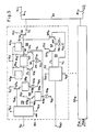
- Fig. 4 shows details for a preferred embodiment of gate 301. The operation of most of the specific circuitry shown in Fig. 4 should be evident to a person skilled in the ECL art, particularly in view of the foregoing discussion. Accordingly, only a brief description of Fig. 4 is given here.
- input circuit 44 is a true-false buffer that produces voltages V HB and V HA respectively at the same and opposite logical values as the difference between voltage V I1 and a reference voltage V BB .
- the core of buffer 44 consists of NPN input transistors Q5 A and Q5 B arranged in a differential configuration, load resistors R5 A and R5 B , and a current source 58.
- a resistor R3 and a PN diode D1 provide gate 301 with protection from electrostatic discharge.
- Level shift 48 A in level-shifting circuit 46 consists of Schottky diodes D1 A and D2 A arranged in series.
- Level shift 48 B similarly consists of Schottky diodes D1 B and D2 B in series.
- Diodes D1 A , D2 A , D1 B , and D2 B are always on during circuit operation.
- V LS thereby equals 2V SH , where V SH is the standard voltage of approximately 0.4 - 0.5 volt that exists across a Schottky diode when it is fully conductive in the forward direction.
- compensation circuit 40 is formed with a resistor R4 and PN diodes D4 and D5.
- Clamp 42 A consists of a PN diode D6 A and Schottky diodes D7 A and D8 A .
- Clamp 42 B similarly consists of a PN diode D6 B and Schottky diodes D7 B and D8 B .
- V CL is equal to V BE + 2V SH since the forward voltage across a fully conductive PN diode is 1V BE .
- each of diodes D6 A and D6 B is preferably implemented as an NPN transistor having its collector shorted to its base.
- V LS is therefore precisely equal to V CL - V BE here.
- control 52 consists of a true-false buffer 60 and a level-shifting circuit 62.
- Buffer 60 compares voltage V OE1 with voltage V BB to generate complementary internal voltages V HE and V HD respectively at the same and opposite logical values as the difference V OE1 - V BB .
- the core of buffer 60 consists of NPN input transistors Q6 D and Q6 E arranged in a differential configuration, load resistors R5 D and R5 E , and a current source 64.
- a resistor R6 and a PN diode D9 provide electrostatic discharge protection.
- Level-shifting circuit 62 is divided into two sections. One of the sections consists of an NPN level-shift transistor Q7 D , Schottky diodes D10 D and D11 D , and a current source 66 D that generate V D by shifting V HD downward by an amount equal to V BE + 2V SH . The other section consists of an NPN level-shift transistor Q7 E , Schottky diodes D10 E and D11 E , and a current source 66 E that generates V E by shifting V HE downward by the same amount. Circuit 62 is, in fact, identical to circuit 44.
- Each of current sources 58, 50 A , 50 B , 26, 64, 66 D , 66 E and 56 is formed with an NPN transistor and a resistor arranged in the conventional manner shown in Fig. 4.
- a common bias voltage V CS is supplied to the bases of these NPN transistors.
- V CC and V EE are 0 volt (ground reference) and -4.5 volts, respectively, in the preferred embodiment of gate 301 .
- V BB and V CS are approximately V CC - 1.3 volts and V EE + 1.3 volts, respectively.
- R1 is 310 ohms.
- Resistors R2 A /R2 B , R3, R4, R5 D /R5 E , and R6 are set at 250, 60,000 400, 250, and 60,000 ohms, respectively.
- the resistors in current sources 58, 50 A /50 B , 26, 64, 66 D /66 E , and 56 are set at 500, 1,000, 150, 500, 250, and 75 ohms, respectively.
- I M and I F are 3 and 6 milliamperes, respectively. As a result, V CL is quite close to I F R1.
- each of resistors R T1 and R T2 is set at 50 ohms.
- V TT is V CC - 2.0 volts.
- the composite system of Figs. 3 and 4 thus operates over the normal ECL output voltage range.
- An intermediate signal complementary to signal V ITM could be provided from the Q1 B collector to a further output transistor that drives a further one-bit data bus arranged the same as bus 32.
- a differential amplifier analogous to amplifier 54 could then be used to place the further output transistor in the three-state mode in response to signal V OE1 .
Landscapes
- Engineering & Computer Science (AREA)
- Power Engineering (AREA)
- Physics & Mathematics (AREA)
- Computer Hardware Design (AREA)
- Computing Systems (AREA)
- General Engineering & Computer Science (AREA)
- Mathematical Physics (AREA)
- Logic Circuits (AREA)
Abstract
Description
- This invention relates generally to electronic circuits using emitter-coupled logic (ECL) and, in particular, to an ECL circuit capable of operating in the three-state mode.
- The term "three-state" as used to describe a digital circuit that drives further circuitry refers to a specific operational mode in which the digital circuit is electronically disconnected from the further circuitry without being physically disconnected from it. More precisely, the digital circuit has an output terminal from which information is supplied to an input point of the further circuitry. While continuing to accept and process input data, the digital circuit can be switched from (a) condition in which the output terminal exhibits low impedance to the further circuitry as the digital circuit switches between a pair of binary logic states to (b) a condition in which the output terminal exhibits very high impedance to the further circuitry. The latter condition is the third state. Due to the high output impedance, the input point of the further circuitry is effectively disconnected from the output terminal.
- Three-state is highly advantageous when the further circuitry is driven by a number of digital circuits, only one of which provides information intended to drive the further circuitry at any given time. By placing the other circuits in the three-state mode, they do not load the further circuitry. This allows it to operate more efficiently. Use of three-state also avoids undesirable interactions among the digital circuits by way of the further circuitry.
- A better understanding of three-state is facilitated with the assistance of Fig. 1 which illustrates how it is typically used with transistor-transistor logic (TTL). Fig. 1 shows a prior art system containing M three-state logic circuits 10₁ - 10M, of which at least circuit 10₁ is a TTL gate. Circuits 10₁ - 10M provide a one-
bit data bus 12 with digital information in response to digital input signals VI1 - VIM and output enabling signals VOE1 - VOEM. Data bus 12 is terminated by resistors RTC and RTE to respective sources of high and low supply voltages VCC and VEE.
The VOE signals for all but one of circuits 10₁ - 10M are normally at output disabling values that place those M-1 circuits in the three-state mode to electrically disconnect their output terminals frombus 12. The VOE signal for the remaining one of circuits 10₁ - 10M is at an output enabling value. This enablesbus 12 to accept its output signal. - Turning specifically to circuit 10₁, it consists of (1) a
TTL input stage 14, (b) aTTL output stage 16 formed with NPN transistors QA, QB, QC, and QD and resistors RA, RB, RC, and RD, and (c) a three-state switching stage 18 formed with acontrol circuit 20 and an NPN transistor QE. Gate 10₁ provides its output signal at an output terminal TO connected tobus 12. When signal VOE1 is at the output enabling value,control 20 maintains transistor QE in the off condition to prevent it from affectingoutput stage 16. Depending on the value of signal VI1, one of output transistors QC and QD is on while the other is off. his defines two logic states. In both cases, current flows through terminal TO, so that it exhibits low output impedance. -
Control 20 turns transistor QE on when signal VOE1 is switched to the output disabling value. This causes transistors QA and QB to turn off regardless of their prior conductive conditions which, in turn, similarly causes both of output transistors QC and QD to turn off. Circuit 10₁ goes into the three-state mode. Substantially no current flows through terminal TO. It now presents a very high output impedance. The presence of two serially connected output transistors make TTL very conductive to three-state. - The situation is quite different with ECL. For example, consider Fig. 2a which illustrates how a conventional
ECL output stage 22 interfaces with a one-bit data bus 24.Stage 22 centers around main NPN transistors Q1A and Q1B whose bases respectively receive base input signals VA and VB. The emitters of transistors Q1A and Q1B are connected together at a node N1 in a differential configuration. Their collectors are respectively coupled through small equal-size load resistors R1A and R1B to the VCCsupply. A maincurrent source 26 connected between node N1 and the VEE supply provides a main supply current IM for transistors Q1A and Q1B. An intermediate voltage signal VITM representative of the state ofstage 22 is taken from a node N2 at the Q1A collector. - Intermediate signal VITM is supplied to the base of an NPN output transistor Q2 whose collector is tied to the VCC supply. Transistor Q2 is always on during circuit operation.
Stage 22 provides its output signal tobus 24 by way of terminal TO connected to the Q2 emitter. The signal voltage onbus 24 is thus about 1VBE and VITM. VBE is the standard voltage of 0.7 - 0.8 volt that exists across the base-emitter junction of a bipolar transistor when it just reaches full conduction in the forward direction.Bus 24 is terminated by a resistor RT to a source of a termination voltage VTT which is usually about 2 volts below VCC. -
Stage 22 is at a high binary stage (or logical"1") when transistor Q1A is off and transistor Q1B is on. This usually arises when the voltage difference VB - VA is about 100 millivolts. None of supply current IM flows through resistor R1A. The only current flowing through resistor R1A is the small current needed to drive the Q2 base. As a result, voltage VITM is at a high level near VCC. Because transis tor Q2 is on, current flows through terminal TO causing it to exhibit a low impedance to bus 24. -
Stage 22 goes into a low binary state (or logical "O") when VB - VA is reversed so as to turn transistor Q1A on and turn transistor Q1B off. All of current IM flows through resistor R1A. Voltage VITM drops to a low level approximately equal to VCC - IMR₁, where R₁ is the resistance of resistor R1A or R1B. The voltage swing INR₁ is typically in the neighborhood of 1VBE. Terminal TO exhibits a low impedance tobus 24.Stage 22 thus switches between two binary logic states, both at low output impedance. - Applying three-state to ECL is a tough problem, largely because there is only one output transistor rather than two as in TTL. Gustafson et al, "ECL Enhances Proven Parallel Architecture, "Northcon/85, 22- 24 October 1985, pp. 1 - 3, discusses some of the difficulties that arise in trying to solve the problem. As a solution, Gustafson et al describe a system in which a "wired-OR" arrangement is combined with bus drivers that provide high output impedance when they are in the low logic state. This system is relatively complex and does not appear particularly efficient or fast. Moreover, it does not truly use three-state.
- This Signetics 100123 ECL integrated circuit is a bus driver of the type employed in Gustafson et al. With reference to Fig. 2a, voltage swing IMR₁ is raised to double its normal value in
output stage 22 of the Signetics 100123. This enables transistor Q2 to turn off whenstage 22 is in the low (but not the high) logic state. Terminal TO presents a high impedance to bus 24 during that time. Even though the Signetics 100123 still operates in only two different states, it does achieve some of the advantages of three-state. However, the increased voltage and the charging/discharging of the Q2 base during normal switching cause the Signetics 100123 to operate significantly slower than an otherwise comparable ECL device. - In explanation of how wired-OR is used in ECL, Fig. 2b illustrates an
ECL output stage 28 having a wired-OR capability.Stage 28 is the same asstage 22 depicted in Fig. 2a except that an NPN transistor Q1C is connected between node N1 and the Q1B collector. A control voltage VC is supplied to the Q1C base. - Transistor Q1C turns on when VC is raised to a suitable high value. All of current IM flows through resistor R1B. VITM thereby goes to its high level irrespective of the values of VA and VB. Alternatively, the Q1B collector could be connected to the Q1A collector. VITM would then go unilaterally to its low level. The wired-OR arrangement comes close to three-state in the sense that
stage 28 can be placed at either a high logic state or a low logic state regardless of the values of VA and VB. However, wired-OR does not provide a true three-state capability in which there are two binary states at low output impedance and one state at high output impedance. - ECL operates much faster than TTL. Accordingly, it would be highly desirable to have an ECL circuit that can be operated in the three-state mode over the normal ECL output voltage range extending from VCC - 2 volts to VCC.
- The present invention is logic circuit that provides such a capability.
- The core of this circuit consists of first and second like-polarity bipolar transistors arranged in a differential configuration. The first transistor has a base that receives an input voltage, an emitter coupled to a first node, and a collector coupled to a second node at which an intermediate voltage signal representative of the state of the circuit is provided. The second transistor has a base that receives another input voltage, an emitter coupled to the first node, and a collector coupled to a source of a first supply voltage. A current source coupled between the first node and a source of a second supply voltage provides a main supply current at the first node. A resistor is coupled between the second node and the source of the first supply voltage.
- The intermediate signal is at a first voltage level representing a first logic state when the first transistor is off and the second transistor is on so that largely none of the main supply current flows through the resistor. The intermediate signal is at a second voltage level representing a second logic state when the first transistor is on and the second transistor is off so that largely all of the main supply current flows through the resistor. The second voltage level is closer to the second supply voltage than the first voltage level.
- The circuit contains a like-polarity bipolar output transistor having a base coupled to the second node, an emitter coupled to an output terminal, and a collector coupled to a voltage source. The output transistor is turned on when the intermediate signal is at the first or second voltage level. The output terminal thereby exhibits low impedance to further circuitry driven from the output terminal.
- A switching stage controls the intermediate signal in response to that output control signal. When the control signal is at a specified condition, the switching stage causes current exceeding the main supply current to flow through the resistor irrespective of the conductive conditions of the first and second transistors. Consequently, the intermediate signal reaches a voltage closer to the second supply voltage than the second level. This places the circuit in a third state.
- An important function is performed by the further circuitry. It prevents the voltage at the output terminal from getting any closer to the second supply voltage than a termination voltage that lies between the supply voltages. The termination voltage is sufficiently close to the first supply voltage that the output transistor turns off when the control signal reaches the specified condition. The output terminal then exhibits very high impedance to the further circuitry, effectively disconnecting it from the logic circuit. In this way, the present ECL circuit achieves a true three-state capability over the portion of the supply voltage range extending between the first supply voltage and the termination voltage.
-
- Fig. 1 is a circuit/block diagram of a prior art bus system containing at least one TTL circuit that operates in the three-state mode.
- Figs. 2a and 2b are circuit diagrams of prior art ECL output stages.
- Fig. 3 is a circuit/block diagram of a bus system containing at least one ECL circuit capable of operating in the three-state mode in accordance with the invention.
- Fig. 4 is a circuit diagram illustrating further details of one ECL circuit in Fig. 3.
- Like reference symbols are employed in the drawings and in the description of the preferred embodiments to represent the same or very similar item or items.
- Referring to Fig. 3, it illustrates an example of a system capable of achieving three-state with ECL. This system is formed with M three-state logic circuits 30₁ - 30M, of which at
least circuit 30₁ is an ECL gate. Circuits 30₁ - 30M operate as a group in response to digital input signals VI1 and VIM and output enabling signals VOE1 and VOEM to control the information transmitted on a one-bit data bus 32 in the same way that circuits 10₁ - 10M in Fig. 1 control the data transmitted onbus 12. -
Bus 32 is preferably terminated at both ends through equal valve resistors RT1 and RT2 to the VTT termination supply. Alternatively,bus 32 could be arranged as shown in Fig. 2a or 2b forbus 24. In either case, termination voltage VTT lies between supply voltages VCC and VEE. -
ECL circuit 30₁ consists of aninput stage 34, anoutput stage 36, and a three-state switching stage 38.Output stage 36 is a good starting point for examining the configuration and operation ofgate 30₁. -
Output stage 36 is a differential amplifier containing main NPN transistors Q1A and Q1B, load resistors R1A and R1B,current source 26, and NPN output transistor Q2 all arranged as in Fig. 2a. Resistor R1A is essential to the circuit design because the voltages defining the states ofcircuit 30₁ are produced across it. For transistor Q2 to be fully conductive when signal VOE1 is at the output enabling value, VCC - VTT - VBE must be greater than the voltage swing IMR₁ across resistor R1A. In contrast, resistor R1B is employed basically to provide "balancing" for atemperature compensation circuit 40 connected between the Q1A and Q1B collectors.Compensation circuit 40 stabilizes the circuit output signal against temperature variations. - A voltage clamp 42A is connected between the VCC supply and the Q1A collector (or node N2). Clamp 42A prevents the voltage across resistor R1A from exceeding a clamped value VCL. For reasons dealt with below, VCL is greater than VCC - VTT - VBE. Another voltage clamp 42B connected between the VCC supply and the Q1B collector prevents the voltage across resistor R1B from exceeding VCL. Clamp 42B rarely becomes active. It basically "balances" clamp 42A to allow
circuit 40 to operate efficiently. - When signal VOE1 is at the output enabling value,
stage 36 operates in the manner described above forstage 22 in Fig. 2a. Clamps 42A and 42B are inactive since VCL is greater than IMR₁. When transistor Q1Ais off and transistor Q1B is on so that largely none of supply current IM flows through resistor R1A, intermediate voltage VITM reaches a high level near VCC representing the high binary state. VITM drops to a low value approximately equal to VCC - IMR₁ representing the low binary state when transistor Q1A is on and transistor Q1B is off so that largely none of current IM flows through resistor R1A. -
Transistor 22 is turned on during the times that VITM switches between VCC and VCC - IMR₁. - Consequently, terminal TO exhibits low impedance to
bus 32. - Moving back to
input stage 34, it consists of anECL input circuit 44 and a level-shiftingcircuit 46. In response to input signal VI1,input circuit 44 generates complentary input voltages VHA and VHB that vary from a low value VHMIN lying between VCC and VEE to a high value near VCC. VHMIN is usually about 1VBE below VCC. Level-shiftingcircuit 46 produces base input voltages VA and VB by respectively shifting voltages VHA and VHB downward by an amount equal to 1VBE plus an additional level shift VLS. Consequently, voltages VA and VB are complementary signals that vary from VHMIN - VBE - VLS approximately to VCC - VBE - VLS. -
Circuit 46 is divided into two identical sections. One of the sections is formed with an NPN level-shift transistor Q3A that provides a downshift equal to 1VBE, a level-shift element 48A that provides a downshift equal to VLS, and a current source 50A connected between a node N3A and the VEE supply. The other section is similarly formed with an NPN level-shift transistor Q3B that provides a 1VBE downshift, a level-shift element 48B that provides a VLS downshift, and a current source 50B connected between a node N3B and the VEE supply. Voltages VHA and VHB are respectively supplied to the bases of transistors Q3A and Q3B whose collectors are tied to the VCC supply. Level-shift elements 48A and 48B are respectively connected between the emitters of transistors Q3A and Q3B and nodes N3A and N3B from which voltages VA and VB are taken. - Level shifts 48A and 48B operate in conjunction with clamp 42A to prevent transistor Q1A from going into deep saturation when signal VOE1 is at the output disabling value -- i.e.,
gate 30₁ is in the three-state mode. This avoids a loss in response time that might otherwise occur when VOE1 is switched to the output enabling value to removecircuit 30₁ from the three-state mode. - In particular, VLS satisfies the relationship
VLS > VCL - VBE - VSV (1)
where VSV is the maximum tolerable forward voltage from the base of transistor Q1A to its collector. Since transistor Q1A goes into deep saturation when its base-to-collector voltage reaches 1VBE , VSV is somewhat less than 1VBE. SSV is usually no more than 0.5 volt and is preferably close to 0 volt. Good operation occurs when VLS equals VCL - VBE. Level shifts 48A and 48B similarly operate in combination with clamp 42B to prevent transistor Q1B from going into deep saturation. -
Switching circuit 38 consists of acontrol circuit 52 and adifferential amplifier 54.Control circuit 52 produces complementary flow-control voltages VD and DE in response to signal VOE1.Differential amplifier 54 is formed with flow transistors Q4D and Q4E and acurrent source 56 connected between the VEE supply and a node N4. Voltages VD and VE are respectively supplied to the control electrodes of transistors Q4D and Q4E which have first flow electrodes connected to node N4 to receive a further supply current IF fromcurrent source 56. Transistor Q4D has a second flow electrode connected to node N2. Transistor Q4E has a second flow electrode tied to the VCC supply. - Transistors Q4D and Q4E are preferably NPN transistors as indicated in Fig. 3. The first, second, and control electrodes of each transistor Q4D or Q4E are then respectively its emitter, collector, and base. Alternatively transistors Q4D and Q4E might be N-channel field-effect transistors of the insulated-gate or junction type. In this case, the source, drain, and gate electrode are respectively the first, second, and control electrodes of each transistor Q4D or Q4E.
-
Switching circuit 38 operates in the following way. When signal VOE1 is at the output disabling value,control circuit 52 produces voltages VE and VD at respective high and low values. Transistor Q4E is turned on. Transistor Q4D is turned off to preventcircuit 38 from affecting the operation ofoutput stage 36. -
Control 52 reverses the values of VD and VE when VOE1 is switched to the output disabling value. Transistor Q4E turns off. Transistor Q4D turns on and draws at least part of further supply current IF through resistor R1A. The circuit parameters are chosen in such a way that current greater than main supply current IM flows through resistor R1A regardless of the conditions of transistors Q1A and Q1B. Signal VITM drops to a voltage below VCC - IMR₁. This placescircuit 30₁ in a third state. - For
gate 30₁ to be electrically disconnected frombus 32, transistor Q2 must turn off irrespective of the condition ofbus 32 and irrespective of the conductive conditions of transistors Q1A and Q1B . The "worst case" arises when transistor Q1A is off and the bus voltage equals VTT. This is the situation in which the current that transistor Q4D draws through resistor R1A in order to force VITM to a voltage low enough to turn off transistor Q2 is at its maximum value IFR. - Clamp 42A may be active or inactive in the "worst case". If clamp 42A is active, it draws part of current IF. Consequently, IF is greater than IFR. If clamp 42A is inactive, IF approximately equals IFR.
- Transistor Q2 turns off when its base-to-emitter voltage drops below 1VBE. IFRR₁ must thus be greater than VCC - VTT - VBE. Taking note of the above-mentioned relationship involving VTT and IM, it follows that:
IFRR₁> VCC - VTT - VBE > IMR₁ (2)
By choosing VTT and IFR according to Eq. (2), transistor Q2 always turns off whenever VOE1 is placed at the output disabling value.Circuit 30₁ goes into a true three-state mode. Terminal TO exhibits very high impedance tobus 32. - If transistor Q1A is turned on when
gate 30₁ is in the three-state mode, clamp 42A becomes active. This increases the circuit switching speed by preventing VITM from going to a voltage much less than that needed to turn transistor Q2 off. - VCL is necessarily less than (IM + IF)R₁. Otherwise, clamp 42A could not turn on. To turn transistor Q2 off, VCL must be greater than VCC - VTT - VBE (as mentioned above). As a result, VCL satisfies the relationship:
(IM + IF)R₁> VCL VCC - VTT - VBE > IMR₁ (3)
VCL is ideally equal to IFR₁. Clamp 42A then becomes active when transistor Q1A is turned on but not when it is turned off. That is, VITM reaches approximately the same voltage regardless of the conductive conditions of transistors Q1A and Q1B. This provides the fastest overall switching speed. - Fig. 4 shows details for a preferred embodiment of
gate 30₁. The operation of most of the specific circuitry shown in Fig. 4 should be evident to a person skilled in the ECL art, particularly in view of the foregoing discussion.
Accordingly, only a brief description of Fig. 4 is given here. - Starting with
input stage 34,input circuit 44 is a true-false buffer that produces voltages VHB and VHA respectively at the same and opposite logical values as the difference between voltage VI1 and a reference voltage VBB. The core ofbuffer 44 consists of NPN input transistors Q5A and Q5B arranged in a differential configuration, load resistors R5A and R5B, and acurrent source 58. A resistor R3 and a PN diode D1 providegate 30₁ with protection from electrostatic discharge. - Level shift 48A in level-shifting
circuit 46 consists of Schottky diodes D1A and D2A arranged in series. Level shift 48B similarly consists of Schottky diodes D1B and D2B in series. Diodes D1A, D2A, D1B, and D2B are always on during circuit operation. VLS thereby equals 2VSH, where VSH is the standard voltage of approximately 0.4 - 0.5 volt that exists across a Schottky diode when it is fully conductive in the forward direction. - Moving to
output stage 36,compensation circuit 40 is formed with a resistor R4 and PN diodes D4 and D5. Clamp 42A consists of a PN diode D6A and Schottky diodes D7A and D8A. Clamp 42B similarly consists of a PN diode D6B and Schottky diodes D7B and D8B. VCL is equal to VBE + 2VSH since the forward voltage across a fully conductive PN diode is 1VBE. In fact each of diodes D6A and D6B is preferably implemented as an NPN transistor having its collector shorted to its base. VLS is therefore precisely equal to VCL - VBE here. - Turning to switching
circuit 38,control 52 consists of a true-false buffer 60 and a level-shifting circuit 62.Buffer 60 compares voltage VOE1 with voltage VBB to generate complementary internal voltages VHE and VHD respectively at the same and opposite logical values as the difference VOE1 - VBB. The core ofbuffer 60 consists of NPN input transistors Q6D and Q6E arranged in a differential configuration, load resistors R5D and R5E, and acurrent source 64. A resistor R6 and a PN diode D9 provide electrostatic discharge protection. - Level-shifting circuit 62 is divided into two sections. One of the sections consists of an NPN level-shift transistor Q7D, Schottky diodes D10D and D11D, and a current source 66D that generate VD by shifting VHD downward by an amount equal to VBE + 2VSH. The other section consists of an NPN level-shift transistor Q7E, Schottky diodes D10E and D11E, and a current source 66E that generates VE by shifting VHE downward by the same amount. Circuit 62 is, in fact, identical to
circuit 44. - Each of
current sources - VCC and VEE are 0 volt (ground reference) and -4.5 volts, respectively, in the preferred embodiment of
gate 30₁ . VBB and VCS are approximately VCC - 1.3 volts and VEE + 1.3 volts, respectively. R₁ is 310 ohms. Resistors R2A/R2B, R3, R4, R5D/R5E, and R6 are set at 250, 60,000 400, 250, and 60,000 ohms, respectively. The resistors incurrent sources 58, 50A/50B, 26, 64, 66D/66E, and 56 are set at 500, 1,000, 150, 500, 250, and 75 ohms, respectively. IM and IF are 3 and 6 milliamperes, respectively. As a result, VCL is quite close to IFR₁. - As to
bus 32, each of resistors RT1 and RT2 is set at 50 ohms. VTT is VCC - 2.0 volts. The composite system of Figs. 3 and 4 thus operates over the normal ECL output voltage range. - While the invention has been described with reference to particular embodiments, this description is solely for the purpose of illustration and is not to be construed as limiting the scope of the invention claimed below. For example, semiconductor elements of opposite polarity to those described above may be used to achieve the same results. The clamps and level-shift elements can be formed with different numbers and types of diodes than those used in the preferred embodiment.
- An intermediate signal complementary to signal VITM could be provided from the Q1B collector to a further output transistor that drives a further one-bit data bus arranged the same as
bus 32. A differential amplifier analogous toamplifier 54 could then be used to place the further output transistor in the three-state mode in response to signal VOE1. Various applications, modifications, and changes may thus be made by those skilled in the art without departing from the true scope and spirit of the invention as described by the appended claims.
Claims (19)
IFRR₁ > VCC - VTT - VBE > IMR₁
where IFR is the magnitude of the maximum current that the switching means draws through the resistor when the first transistor is off, R₁ is the resistance of the resistor, VCC - VTT is the magnitude of the difference between the first supply voltage and the termination voltage, VBE is the magnitude of the standard voltage across the base-emitter junction of a bipolar transistor when it just reaches full conduction in the forward direction, and IM is the magnitude of the main supply current.
a flow transistor having a first flow electrode coupled to a further node, a second flow electrode coupled to the second node, and a control electrode responsive to a flow-control voltage for controlling current transmissions between the flow electrodes; and
a further current source, coupled between the further node and the source of the second supply voltage, for providing a further supply current at the further node.
a further flow transistor having a first flow electrode coupled to the further node, a second flow electrode coupled to a voltage source, and a control electrode responsive to a further flow-control voltage for controlling current transmission between the flow electrodes of the further transistor; and
control means responsive to the output control signal for generating the flow-control voltages.
(IM + IF)R₁> VCL > VCC - VTT - VBE > IMR₁
where IM is the magnitude of the main supply current, IF is the magnitude of the further supply current, R₁ is the resistance of the resistor, VCC - VTT is the magnitude of the difference between the first supply voltage and the termination voltage, and VBE is the magnitude of the voltage across the base-emitter junction of a bipolar transistor when it just reaches full conduction in the forward direction.
a like-polarity level-shift bipolar transistor having a base that receives a different one of the internal voltages, an emitter, and a collector coupled to a voltage source; and
a level-shift element coupled between the emitter of the level-shift transistor and a node coupled to the base of a different one of the main transistors.
the clamp prevents the magnitude of the voltage across the resistor from exceeding a value VCL that satisfies the relationship:
(IM + IF)R₁ > VCL > VCC - VTT - VBE > IMR₁
where IM is the magnitude of the main supply current, IF is the magnitude of the further supply current, R₁ is the resistance of the resistor, VCC - VTT is the magnitude of the difference between the first supply voltage and the termination voltage, and VBE is the magnitude of the voltage across the base-emitter junction of a bipolar transistor when it just reaches full conduction in the forward direction; and each level-shift element produces a level-shift voltage having a magnitude VLS that satisfies the relationship
VLS > VCL - VBE - VSV
where VSV is the magnitude of the maximum tolerable forward voltage between the base and collector of the first transistor.
Applications Claiming Priority (2)
| Application Number | Priority Date | Filing Date | Title |
|---|---|---|---|
| US07/132,377 US4849659A (en) | 1987-12-15 | 1987-12-15 | Emitter-coupled logic circuit with three-state capability |
| US132377 | 1987-12-15 |
Publications (2)
| Publication Number | Publication Date |
|---|---|
| EP0321028A2 true EP0321028A2 (en) | 1989-06-21 |
| EP0321028A3 EP0321028A3 (en) | 1989-10-25 |
Family
ID=22453742
Family Applications (1)
| Application Number | Title | Priority Date | Filing Date |
|---|---|---|---|
| EP88202821A Ceased EP0321028A3 (en) | 1987-12-15 | 1988-12-09 | Emitter-coupled logic circuit with three-state capability |
Country Status (4)
| Country | Link |
|---|---|
| US (1) | US4849659A (en) |
| EP (1) | EP0321028A3 (en) |
| JP (1) | JPH022711A (en) |
| KR (1) | KR890011217A (en) |
Cited By (2)
| Publication number | Priority date | Publication date | Assignee | Title |
|---|---|---|---|---|
| EP0425951A3 (en) * | 1989-11-01 | 1991-07-17 | National Semiconductor Corporation | Ecl cutoff driver circuit with reduced standby power dissipation |
| EP0417617A3 (en) * | 1989-09-15 | 1992-05-06 | National Semiconductor Corporation | Ecl clamped cut-off driver |
Families Citing this family (20)
| Publication number | Priority date | Publication date | Assignee | Title |
|---|---|---|---|---|
| DE3871660T2 (en) * | 1987-08-26 | 1993-01-21 | Japan Res Dev Corp | METHOD FOR PRODUCING A GRAPHITE FILM OR SHEET AND RADIATION-OPTICAL DEVICE USING THE GRAPHITE SHEET. |
| JPH01278041A (en) * | 1988-04-30 | 1989-11-08 | Hitachi Ltd | Semiconductor integrated circuit device |
| US4891535A (en) * | 1988-12-20 | 1990-01-02 | Tektronix, Inc. | Single supply ECL to CMOS converter |
| US5280200A (en) * | 1989-04-10 | 1994-01-18 | Tarng Min M | Pipelined buffer for analog signal and power supply |
| US5028820A (en) * | 1989-06-23 | 1991-07-02 | Digital Equipment Corporation | Series terminated ECL buffer circuit and method with an optimized temperature compensated output voltage swing |
| US4939393A (en) * | 1989-10-02 | 1990-07-03 | Motorola Inc. | ECL to TTL/CMOS translator using a single power supply |
| JPH03166821A (en) * | 1989-11-27 | 1991-07-18 | Hitachi Ltd | Semiconductor integrated circuit device |
| US5248909A (en) * | 1990-01-09 | 1993-09-28 | Fujitsu Limited | ECL-TO-GaAs level converting circuit |
| JP2545146B2 (en) * | 1990-01-25 | 1996-10-16 | 富士通株式会社 | Level conversion circuit |
| US5101123A (en) * | 1990-06-29 | 1992-03-31 | Texas Instruments Incorporated | CMOS to ECL translator circuit and methodology |
| US5381060A (en) * | 1992-02-14 | 1995-01-10 | International Business Machines Corporation | Differential current switch to super buffer logic level translator |
| JPH07123225B2 (en) * | 1992-03-26 | 1995-12-25 | 日本電気株式会社 | Wired or logic circuit |
| DE69334054T2 (en) * | 1992-06-15 | 2006-12-07 | Fujitsu Ltd., Kawasaki | Integrated semiconductor circuit with input / output interface suitable for low amplitudes |
| US5315179A (en) * | 1992-09-28 | 1994-05-24 | Motorola, Inc. | BICMOS level converter circuit |
| TW307064B (en) * | 1993-09-08 | 1997-06-01 | Advanced Micro Devices Inc | |
| US5424658A (en) * | 1993-12-10 | 1995-06-13 | Cray Research, Inc. | Bipolar ECL to inverted CMOS level translator |
| US6310489B1 (en) * | 1996-04-30 | 2001-10-30 | Sun Microsystems, Inc. | Method to reduce wire-or glitch in high performance bus design to improve bus performance |
| US7142132B2 (en) * | 2004-11-09 | 2006-11-28 | General Motors Corporation | Methods and systems for multi-state switching using at least one ternary input and at least one discrete input |
| US9276529B1 (en) * | 2014-10-03 | 2016-03-01 | Hrl Laboratories, Llc | High performance GaN operational amplifier with wide bandwidth and high dynamic range |
| CN110047266B (en) * | 2018-01-17 | 2021-01-22 | 京东方科技集团股份有限公司 | Information representation method, multi-system calculation circuit and electronic system |
Family Cites Families (9)
| Publication number | Priority date | Publication date | Assignee | Title |
|---|---|---|---|---|
| US29982A (en) * | 1860-09-11 | Saw-tooth | ||
| US3602733A (en) | 1969-04-16 | 1971-08-31 | Signetics Corp | Three output level logic circuit |
| JPS4818671B1 (en) * | 1969-06-06 | 1973-06-07 | ||
| US3630990A (en) * | 1970-01-09 | 1971-12-28 | Eastman Kodak Co | Textile fibers |
| US4490630A (en) * | 1982-06-30 | 1984-12-25 | International Business Machines Corporation | Current switch emitter follower with current mirror coupled push-pull output stage |
| GB2128432B (en) * | 1982-09-28 | 1986-07-30 | Monolithic Memories Inc | Improvements in or relating to a tri-state output circuit |
| US4596940A (en) * | 1984-04-19 | 1986-06-24 | Hewlett-Packard Company | Three state differential ECL bus driver |
| US4751406A (en) * | 1985-05-03 | 1988-06-14 | Advanced Micro Devices, Inc. | ECL circuit with output transistor auxiliary biasing circuit |
| US4682058A (en) * | 1986-07-03 | 1987-07-21 | Unisys Corporation | Three-state logic circuit for wire-ORing to a data bus |
-
1987
- 1987-12-15 US US07/132,377 patent/US4849659A/en not_active Expired - Fee Related
-
1988
- 1988-12-09 EP EP88202821A patent/EP0321028A3/en not_active Ceased
- 1988-12-13 JP JP63314815A patent/JPH022711A/en active Pending
- 1988-12-14 KR KR1019880016634A patent/KR890011217A/en not_active Withdrawn
Cited By (2)
| Publication number | Priority date | Publication date | Assignee | Title |
|---|---|---|---|---|
| EP0417617A3 (en) * | 1989-09-15 | 1992-05-06 | National Semiconductor Corporation | Ecl clamped cut-off driver |
| EP0425951A3 (en) * | 1989-11-01 | 1991-07-17 | National Semiconductor Corporation | Ecl cutoff driver circuit with reduced standby power dissipation |
Also Published As
| Publication number | Publication date |
|---|---|
| JPH022711A (en) | 1990-01-08 |
| US4849659A (en) | 1989-07-18 |
| KR890011217A (en) | 1989-08-14 |
| EP0321028A3 (en) | 1989-10-25 |
Similar Documents
| Publication | Publication Date | Title |
|---|---|---|
| US4849659A (en) | Emitter-coupled logic circuit with three-state capability | |
| GB2156614A (en) | A switching circuit | |
| US3766406A (en) | Ecl-to-ttl converter | |
| EP0137844B1 (en) | Ttl-ecl input translation with and/nand function | |
| JPH0261817B2 (en) | ||
| US4943740A (en) | Ultra fast logic | |
| US5202594A (en) | Low power level converter | |
| EP0590247B1 (en) | BICMOS level converter circuit | |
| EP0590246A2 (en) | Power supply dependent input buffer | |
| US3942033A (en) | Current mode logic circuit | |
| EP0193459B1 (en) | Ttl tristate output device | |
| US4578602A (en) | Voltage signal translator | |
| US5349253A (en) | Logic translator interfacing between five-volt TTL/CMOS and three-volt CML | |
| US3723761A (en) | Emitter-emitter coupled logic circuit device | |
| EP0027860A1 (en) | Complementary transistor, inverting emitter follower circuit | |
| US5945848A (en) | Effectively differential, multiple input OR/NOR gate architecture | |
| US5331225A (en) | BiCMOS logic circuit with bipolar transistor and MOS transistor formed on the same semiconductor substrate | |
| EP0161015B1 (en) | Input circuit for producing discharge path to enhance operation | |
| US5398000A (en) | Simple and high speed BICMOS tristate buffer circuit | |
| EP0102675A2 (en) | Transistor-transistor logic circuit with hysteresis | |
| JP2833657B2 (en) | Semiconductor integrated circuit device | |
| US4845387A (en) | Non-stacked ECL type and function | |
| US4996452A (en) | ECL/TTL tristate buffer | |
| US5424658A (en) | Bipolar ECL to inverted CMOS level translator | |
| US4868904A (en) | Complementary noise-immune logic |
Legal Events
| Date | Code | Title | Description |
|---|---|---|---|
| PUAI | Public reference made under article 153(3) epc to a published international application that has entered the european phase |
Free format text: ORIGINAL CODE: 0009012 |
|
| AK | Designated contracting states |
Kind code of ref document: A2 Designated state(s): DE FR GB IT NL |
|
| PUAL | Search report despatched |
Free format text: ORIGINAL CODE: 0009013 |
|
| AK | Designated contracting states |
Kind code of ref document: A3 Designated state(s): DE FR GB IT NL |
|
| 17P | Request for examination filed |
Effective date: 19900423 |
|
| 17Q | First examination report despatched |
Effective date: 19910806 |
|
| STAA | Information on the status of an ep patent application or granted ep patent |
Free format text: STATUS: THE APPLICATION HAS BEEN REFUSED |
|
| 18R | Application refused |
Effective date: 19930605 |