EP0321224A2 - Image sensor - Google Patents
Image sensor Download PDFInfo
- Publication number
- EP0321224A2 EP0321224A2 EP88311846A EP88311846A EP0321224A2 EP 0321224 A2 EP0321224 A2 EP 0321224A2 EP 88311846 A EP88311846 A EP 88311846A EP 88311846 A EP88311846 A EP 88311846A EP 0321224 A2 EP0321224 A2 EP 0321224A2
- Authority
- EP
- European Patent Office
- Prior art keywords
- electrode
- light
- electrodes
- light window
- transparent
- Prior art date
- Legal status (The legal status is an assumption and is not a legal conclusion. Google has not performed a legal analysis and makes no representation as to the accuracy of the status listed.)
- Granted
Links
Images


Classifications
-
- H—ELECTRICITY
- H04—ELECTRIC COMMUNICATION TECHNIQUE
- H04N—PICTORIAL COMMUNICATION, e.g. TELEVISION
- H04N1/00—Scanning, transmission or reproduction of documents or the like, e.g. facsimile transmission; Details thereof
- H04N1/024—Details of scanning heads ; Means for illuminating the original
- H04N1/028—Details of scanning heads ; Means for illuminating the original for picture information pick-up
- H04N1/03—Details of scanning heads ; Means for illuminating the original for picture information pick-up with photodetectors arranged in a substantially linear array
- H04N1/031—Details of scanning heads ; Means for illuminating the original for picture information pick-up with photodetectors arranged in a substantially linear array the photodetectors having a one-to-one and optically positive correspondence with the scanned picture elements, e.g. linear contact sensors
- H04N1/0315—Details of scanning heads ; Means for illuminating the original for picture information pick-up with photodetectors arranged in a substantially linear array the photodetectors having a one-to-one and optically positive correspondence with the scanned picture elements, e.g. linear contact sensors using photodetectors and illumination means mounted on separate supports or substrates or mounted in different planes
- H04N1/0316—Details of scanning heads ; Means for illuminating the original for picture information pick-up with photodetectors arranged in a substantially linear array the photodetectors having a one-to-one and optically positive correspondence with the scanned picture elements, e.g. linear contact sensors using photodetectors and illumination means mounted on separate supports or substrates or mounted in different planes illuminating the scanned image elements through the plane of the photodetector, e.g. back-light illumination
-
- H—ELECTRICITY
- H04—ELECTRIC COMMUNICATION TECHNIQUE
- H04N—PICTORIAL COMMUNICATION, e.g. TELEVISION
- H04N1/00—Scanning, transmission or reproduction of documents or the like, e.g. facsimile transmission; Details thereof
- H04N1/024—Details of scanning heads ; Means for illuminating the original
- H04N1/028—Details of scanning heads ; Means for illuminating the original for picture information pick-up
- H04N1/03—Details of scanning heads ; Means for illuminating the original for picture information pick-up with photodetectors arranged in a substantially linear array
- H04N1/031—Details of scanning heads ; Means for illuminating the original for picture information pick-up with photodetectors arranged in a substantially linear array the photodetectors having a one-to-one and optically positive correspondence with the scanned picture elements, e.g. linear contact sensors
- H04N1/0313—Direct contact pick-up heads, i.e. heads having no array of elements to project the scanned image elements onto the photodectors
-
- H—ELECTRICITY
- H10—SEMICONDUCTOR DEVICES; ELECTRIC SOLID-STATE DEVICES NOT OTHERWISE PROVIDED FOR
- H10F—INORGANIC SEMICONDUCTOR DEVICES SENSITIVE TO INFRARED RADIATION, LIGHT, ELECTROMAGNETIC RADIATION OF SHORTER WAVELENGTH OR CORPUSCULAR RADIATION
- H10F39/00—Integrated devices, or assemblies of multiple devices, comprising at least one element covered by group H10F30/00, e.g. radiation detectors comprising photodiode arrays
- H10F39/10—Integrated devices
- H10F39/12—Image sensors
- H10F39/191—Photoconductor image sensors
Definitions
- the present invention relates to image sensors and more particularly, though not exclusively, relates to contact image sensors, that is to say very small photoelectric conversion devices, which have attracted the interest of researchers as efforts have been made to decrease the sizes of facsimile machines, photocopying machines and the like.
- the sensor structure of Fig.1(A) comprises a glass substrate 1, a front light blocking electrode 2, a photosensitive semiconductor film 3, a rear transparent electrode 4, and a transparent protector layer 5 which is to make direct contact with an image carrying original 6.
- a light window 7 is opened in the photoelectric conversion structure consisting of the electrodes 2 and 3 and the semiconductor film 5. Light rays 8 passing through the light window 7 are reflected by the original 6 and absorbed by the semiconductor film 3 for providing output signals representative of the visual information contained in the original 6.
- the photoelectric conversion structure of Fig.1(A) is commonly formed by scribing the triple-layered laminae consisting of the electrodes 2 and 4 and the semiconductor film 3, and consequently there is a risk that short circuiting paths may be formed across the opposed electrodes 2 and 4 during the simultaneous scribing of the multiple layers.
- the sensor illustrated in Fig.1(B) is constructed similarly to the structure of Fig.1(A) except that a metallic electrode 9 is deposited on the semiconductor film 3 after scribing of the semiconductor film 3 and the underlying light blocking electrode 2.
- a metallic electrode 9 is deposited on the semiconductor film 3 after scribing of the semiconductor film 3 and the underlying light blocking electrode 2.
- the formation of short circuit paths between the electrodes 9 and 2 is unlikely in this case.
- This case, however, requires a fine patterning technique capable of fabricating comb electrode structures with adjacent conductive lines separated by several microns intervals.
- an image sensor comprising a photosensitive semiconductor layer sandwiched between a transparent electrode structure on one side of the layer and a light blocking electrode structure on the other side thereof, and wherein a light window is opened through the photosensitive semiconductor layer and the light blocking electrode and one of said electrodes extends over the edges of the semiconductor layer exposed by the light window.
- an image sensor comprising: a transparent substrate; a first electrode formed on said substrate; a photosensitive semiconductor layer formed on said first electrode; a light window provided in said first electrode and in said photosensitive semiconductor layer; a second electrode formed on said photosensitive semiconductor layer and in said light window so as to cover the side surfaces of said semiconductor layer whereat they are exposed by said light window; and a transparent protecting layer covering said second electrode, one of said first and second electrodes being light blocking while the other is transparent and said first and second electrodes being patterned in order to obtain photogenerating signals therebetween.
- an image sensor comprising: a transparent substrate; a light blocking conductive film separated into a plurality of first electrodes by grooves; a photoelectric conversion semiconductor film formed on said light blocking conductive film; light windows opened in said semiconductor film and said light blocking conductive film; a transparent conductive film separated into a plurality of second electrodes by grooves, said second electrodes being formed also in said light windows in order to make contact with said first electrodes, whereby a plurality of photoelectric conversion elements are formed between pairs of said first and second electrodes which are opposed to each other with said semiconductor film therebetween; and a transparent protective layer formed on said transparent conductive film.
- the sensor comprises a glass substrate 1, a light blocking electrode 2 made of an opaque conductive material, a photosensitive amorphous silicon semiconductor film 3, a transparent electrode 4 and a protective layer 5.
- a light window 7 is opened in the semiconductor film 3 and the light blocking electrode 2.
- the transparent electrode 4 is formed so as to extend into the light window 7 and over the side surface 12 of the semiconductor film 3 where it is exposed by the window, and is electrically separated by provision of a groove 10 at a position just adjacent to the light window 7.
- the underlying light blocking electrode 2 is also separated by a groove 9 at a point a certain length distant from the light window 7.
- Fig.2 The diagram of Fig.2 is illustrative only and shows only one complete sensor segment, whereas in reality a plurality of sensing elements as illustrated in the figure are formed in an array, for example in a row, in order to provide a line sensor.
- the deposition and patterning of an opaque conductive film, a semiconductor film and a transparent film are actually performed so that a plurality of photosensitive elements are constructed in an array, each element being composed of a light blocking electrode 2, a semiconductor film 3 and a transparent electrode 4 as illustrated in the figure.
- Output signals from each element can be obtained respectively between the light blocking and transparent electrodes.
- the sensor of Fig.2 can be fabricated in the following manner.
- a chromium film is deposited to a thickness of 500 angstroms by a known sputtering technique and is then subjected to laser scribing with a KrF excimer laser (248nm) in order to define the light blocking electrode 2 which is electrically separated by the groove 9 into the right and left portions shown in the figure.
- the photosensitive amorphous silicon semiconductor film 3 is formed on the electrode 2 by sequentially depositing a 300 ⁇ thick n-type amorphous silicon film, a 6000 ⁇ thick intrinsic amorphous silicon film, and a 300 ⁇ thick p-type amorphous silicon film in this order by a known plasma CVD process.
- the window 7 is opened through the electrode 2 and the semiconductor film 3 by means of the excimer laser.
- a 1000 ⁇ thick ITO film is deposited by sputtering on the semiconductor film 3 and into the opening 7 so as to cover the side surfaces 12 thereof.
- the groove 10 which electrically separates the right and left portions of the ITO (indium tin oxide) film is formed by excimer laser scribing in the same way as the groove 9.
- a 10 microns thick polyimide film protective layer is formed over the structure by a known spinning technique.
- the photosensitive region is located between the grooves 9 and 10 and, by virtue of the electrode covering the sides of the window 7, is immune to the effect of undesirable light rays, which directly enter the semiconductor film without reflecting from the original 6.
- Such light rays directly incident on the edge portion of the film 3 can give rise to free carriers in the semiconductor film, but these will quickly be dissipated by the electrode 4 making contact with the side surface 12 of the film 3 so that little or no noise will be induced in the signals output from the device.
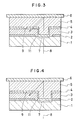
- Fig.3 is a cross sectional view showing a modification of the above described embodiments.
- a 120 microns wide groove is formed in the light blocking electrode 2 before the semiconductor film 3 is deposited and a 100 microns wide light window 7 is opened in the semiconductor film 3.
- the transparent electrode 4 and the light blocking electrode 2 are electrically separated by the intervening semiconductor portion between the light window 7 and the electrode 2.
- a groove 9 is formed at a certain distance from the window 7 so that a photosensitive region is located between the groove 9 and the window 7. In this structure, output signals are obtained between the electrodes 2 and 4.
- Fig.4 is a cross sectional view showing a modification of the structure shown in Fig.3.
- the right hand portion of the light blocking electrode 2 is formed in electrical contact with the transparent electrode 4 at light window 7. Output signals can be obtained between the separated portions of the electrode 2.
Landscapes
- Engineering & Computer Science (AREA)
- Multimedia (AREA)
- Signal Processing (AREA)
- Solid State Image Pick-Up Elements (AREA)
Abstract
Description
- The present invention relates to image sensors and more particularly, though not exclusively, relates to contact image sensors, that is to say very small photoelectric conversion devices, which have attracted the interest of researchers as efforts have been made to decrease the sizes of facsimile machines, photocopying machines and the like.
- Two examples of conventional image sensors are illustrated in Figs.1(A) and 1(B).
- The sensor structure of Fig.1(A) comprises a
glass substrate 1, a frontlight blocking electrode 2, aphotosensitive semiconductor film 3, a reartransparent electrode 4, and atransparent protector layer 5 which is to make direct contact with an image carrying original 6. Alight window 7 is opened in the photoelectric conversion structure consisting of theelectrodes semiconductor film 5.Light rays 8 passing through thelight window 7 are reflected by the original 6 and absorbed by thesemiconductor film 3 for providing output signals representative of the visual information contained in the original 6. - The photoelectric conversion structure of Fig.1(A) is commonly formed by scribing the triple-layered laminae consisting of the
electrodes semiconductor film 3, and consequently there is a risk that short circuiting paths may be formed across theopposed electrodes - The sensor illustrated in Fig.1(B) is constructed similarly to the structure of Fig.1(A) except that a
metallic electrode 9 is deposited on thesemiconductor film 3 after scribing of thesemiconductor film 3 and the underlyinglight blocking electrode 2. The formation of short circuit paths between theelectrodes - Furthermore, in both of the Figs.1(A) and 1(B) devices the problem arises that noise originates as the result of light rays incident upon the
side surfaces 13 of the semiconductor film, such light rays giving rise to carriers in the semiconductor irrespective of whether the original 6 is white or black and consequently reducing the quality of the copy. - It is an object of the present invention to provide an image sensor which overcomes or substantially reduces the abovementioned problems of the prior art sensors.
- According to the present invention in one of its aspects there is provided an image sensor comprising a photosensitive semiconductor layer sandwiched between a transparent electrode structure on one side of the layer and a light blocking electrode structure on the other side thereof, and wherein a light window is opened through the photosensitive semiconductor layer and the light blocking electrode and one of said electrodes extends over the edges of the semiconductor layer exposed by the light window.
- More particularly the present invention provides an image sensor comprising: a transparent substrate; a first electrode formed on said substrate; a photosensitive semiconductor layer formed on said first electrode; a light window provided in said first electrode and in said photosensitive semiconductor layer; a second electrode formed on said photosensitive semiconductor layer and in said light window so as to cover the side surfaces of said semiconductor layer whereat they are exposed by said light window; and a transparent protecting layer covering said second electrode, one of said first and second electrodes being light blocking while the other is transparent and said first and second electrodes being patterned in order to obtain photogenerating signals therebetween.
- According to yet another aspect of the invention there is provided an image sensor comprising: a transparent substrate; a light blocking conductive film separated into a plurality of first electrodes by grooves; a photoelectric conversion semiconductor film formed on said light blocking conductive film; light windows opened in said semiconductor film and said light blocking conductive film; a transparent conductive film separated into a plurality of second electrodes by grooves, said second electrodes being formed also in said light windows in order to make contact with said first electrodes, whereby a plurality of photoelectric conversion elements are formed between pairs of said first and second electrodes which are opposed to each other with said semiconductor film therebetween; and a transparent protective layer formed on said transparent conductive film.
- Further features of the present invention are set forth in the appended claims and, together with the abovementioned features, will become well understood from consideration of the following description given with reference to the accompanying drawings.
-
- Figs.1(A) and 1(B) are cross sectional views showing prior art image sensors;
- Fig.2 is a cross sectional view showing the structure of an exemplary image sensor in accordance with the present invention;
- Fig.3 is a cross sectional view showing a modification of the embodiment illustrated in Fig.2; and
- Fig.4 is a cross sectional view showing a modification of the structure shown in Fig.3.
- Referring now to Fig.2, a gapless type image sensor in accordance with the present invention is illustrated. The sensor comprises a
glass substrate 1, alight blocking electrode 2 made of an opaque conductive material, a photosensitive amorphoussilicon semiconductor film 3, atransparent electrode 4 and aprotective layer 5. Alight window 7 is opened in thesemiconductor film 3 and thelight blocking electrode 2. Thetransparent electrode 4 is formed so as to extend into thelight window 7 and over theside surface 12 of thesemiconductor film 3 where it is exposed by the window, and is electrically separated by provision of agroove 10 at a position just adjacent to thelight window 7. The underlyinglight blocking electrode 2 is also separated by agroove 9 at a point a certain length distant from thelight window 7. - The diagram of Fig.2 is illustrative only and shows only one complete sensor segment, whereas in reality a plurality of sensing elements as illustrated in the figure are formed in an array, for example in a row, in order to provide a line sensor. The deposition and patterning of an opaque conductive film, a semiconductor film and a transparent film are actually performed so that a plurality of photosensitive elements are constructed in an array, each element being composed of a
light blocking electrode 2, asemiconductor film 3 and atransparent electrode 4 as illustrated in the figure. Output signals from each element can be obtained respectively between the light blocking and transparent electrodes. - The sensor of Fig.2 can be fabricated in the following manner. A chromium film is deposited to a thickness of 500 angstroms by a known sputtering technique and is then subjected to laser scribing with a KrF excimer laser (248nm) in order to define the
light blocking electrode 2 which is electrically separated by thegroove 9 into the right and left portions shown in the figure. The photosensitive amorphoussilicon semiconductor film 3 is formed on theelectrode 2 by sequentially depositing a 300 Å thick n-type amorphous silicon film, a 6000 Å thick intrinsic amorphous silicon film, and a 300 Å thick p-type amorphous silicon film in this order by a known plasma CVD process. Thewindow 7 is opened through theelectrode 2 and thesemiconductor film 3 by means of the excimer laser. A 1000 Å thick ITO film is deposited by sputtering on thesemiconductor film 3 and into theopening 7 so as to cover theside surfaces 12 thereof. Thegroove 10 which electrically separates the right and left portions of the ITO (indium tin oxide) film is formed by excimer laser scribing in the same way as thegroove 9. Finally, a 10 microns thick polyimide film protective layer is formed over the structure by a known spinning technique. - In the device of Fig.2, the photosensitive region is located between the
grooves window 7, is immune to the effect of undesirable light rays, which directly enter the semiconductor film without reflecting from the original 6. Such light rays directly incident on the edge portion of thefilm 3 can give rise to free carriers in the semiconductor film, but these will quickly be dissipated by theelectrode 4 making contact with theside surface 12 of thefilm 3 so that little or no noise will be induced in the signals output from the device. - Fig.3 is a cross sectional view showing a modification of the above described embodiments. In the embodiment of Fig.3, a 120 microns wide groove is formed in the
light blocking electrode 2 before thesemiconductor film 3 is deposited and a 100 micronswide light window 7 is opened in thesemiconductor film 3. As may be seen from the figure, thetransparent electrode 4 and thelight blocking electrode 2 are electrically separated by the intervening semiconductor portion between thelight window 7 and theelectrode 2. Agroove 9 is formed at a certain distance from thewindow 7 so that a photosensitive region is located between thegroove 9 and thewindow 7. In this structure, output signals are obtained between theelectrodes - Fig.4 is a cross sectional view showing a modification of the structure shown in Fig.3. In this structure, the right hand portion of the
light blocking electrode 2 is formed in electrical contact with thetransparent electrode 4 atlight window 7. Output signals can be obtained between the separated portions of theelectrode 2. - While several embodiments have been specifically described, it is to be appreciated that the present invention is not limited to the particular examples described and that modifications and variations can be made without departure from the scope of the invention as defined by the appended claims. For example, although the embodiments herein described are constructed with the light blocking electrodes made of chromium, composite electrodes formed of a material such as a laminate consisting of an ITO film and a Mo film for example may be used. In this case, where the constituent ITO film makes contact with the transparent electrode (made also of an ITO film) as in the embodiments of Figs. 2 and 4, the reliability of the electrical connection between the light blocking film and the transparent film is increased.
Claims (10)
- An image sensor comprising a photosensitive semiconductor layer sandwiched between a transparent electrode structure on one side of the layer and a light blocking electrode structure on the other side thereof, and wherein a light window is opened through the photosensitive semiconductor layer and the light blocking electrode and one of said electrodes extends over the edges of the semiconductor layer exposed by the light window.
- An image sensor comprising:a transparent substrate;a first electrode formed on said substrate;a photosensitive semiconductor layer formed on said first electrode;a light window provided in said first electrode and in said photosensitive semiconductor layer;a second electrode formed on said photosensitive semiconductor layer and in said light window so as to cover the side surfaces of said semiconductor layer whereat they are exposed by said light window; anda transparent protecting layer covering said second electrode, one of said first and second electrodes being light blocking while the other is transparent and said first and second electrodes being patterned in order to obtain photogenerating signals therebetween.
- The sensor of claim 2 wherein said first electrode is light blocking and said second electrode is formed of a transparent conductive film extending to cover said light window.
- The sensor of claim 2 or 3 wherein said light window is an opening through said first electrode and said semiconductor film.
- The sensor of claim 4 wherein said opening in said first electrode is formed aligned with said light window.
- The sensor of claim 4 wherein the widths of the opening in said first electrode and of said light window are equal.
- The sensor of claim 4 wherein the width of said opening in said first electrode is larger than that of said light window.
- The sensor of claim 7 wherein the opening in said first electrode is formed so that said first and second electrodes do not make contact with each other at said light window.
- The sensor of claim 7 wherein the opening in said first electrode is formed so as to electrically separate said first electrode into two portions, one of which is isolated from said second electrode and the other of which makes contact with said second electrode at said opening.
- An image sensor comprising:a transparent substrate;a light blocking conductive film separated into a plurality of first electrodes by grooves;a photoelectric conversion semiconductor film formed on said light blocking conductive film:light windows opened in said semiconductor film and said light blocking conductive film;a transparent conductive film separated into a plurality of second electrodes by grooves, said second electrodes being formed also in said light windows in order to make contact with said first electrodes, whereby a plurality of photoelectric conversion elements are formed between pairs of said first and second electrodes which are opposed to each other with said semiconductor film therebetween; anda transparent protective layer formed on said transparent conductive film.
Applications Claiming Priority (4)
| Application Number | Priority Date | Filing Date | Title |
|---|---|---|---|
| JP321689/87 | 1987-12-18 | ||
| JP62321688A JP2639663B2 (en) | 1987-12-18 | 1987-12-18 | Photoelectric conversion element |
| JP62321689A JP2639664B2 (en) | 1987-12-18 | 1987-12-18 | Photoelectric conversion element |
| JP321688/87 | 1987-12-18 |
Publications (3)
| Publication Number | Publication Date |
|---|---|
| EP0321224A2 true EP0321224A2 (en) | 1989-06-21 |
| EP0321224A3 EP0321224A3 (en) | 1990-10-24 |
| EP0321224B1 EP0321224B1 (en) | 1993-08-11 |
Family
ID=26570562
Family Applications (1)
| Application Number | Title | Priority Date | Filing Date |
|---|---|---|---|
| EP88311846A Expired - Lifetime EP0321224B1 (en) | 1987-12-18 | 1988-12-14 | Image sensor |
Country Status (3)
| Country | Link |
|---|---|
| US (1) | US5014100A (en) |
| EP (1) | EP0321224B1 (en) |
| DE (1) | DE3883184T2 (en) |
Families Citing this family (6)
| Publication number | Priority date | Publication date | Assignee | Title |
|---|---|---|---|---|
| US5627364A (en) * | 1994-10-11 | 1997-05-06 | Tdk Corporation | Linear array image sensor with thin-film light emission element light source |
| US6596401B1 (en) | 1998-11-10 | 2003-07-22 | C. R. Bard Inc. | Silane copolymer compositions containing active agents |
| TW583703B (en) * | 2002-10-11 | 2004-04-11 | High Link Technology Corp | Optoelectronic unit and transparent conductive substrate of the same |
| EP2416376A4 (en) * | 2009-03-31 | 2017-07-05 | LG Innotek Co., Ltd. | Solar photovoltaic power generation apparatus and manufacturing method thereof |
| KR20130109786A (en) * | 2012-03-28 | 2013-10-08 | 삼성에스디아이 주식회사 | Solar cell and manufacturing method thereof |
| CN206114183U (en) * | 2016-10-13 | 2017-04-19 | 深圳市大疆创新科技有限公司 | Sensing element and have this sensing element's electron device , unmanned aerial vehicle |
Family Cites Families (2)
| Publication number | Priority date | Publication date | Assignee | Title |
|---|---|---|---|---|
| US4527006A (en) * | 1982-11-24 | 1985-07-02 | Semiconductor Energy Laboratory Co., Ltd. | Photoelectric conversion device |
| DE3789846T2 (en) * | 1986-10-07 | 1994-09-22 | Canon Kk | Image reading system. |
-
1988
- 1988-12-14 DE DE88311846T patent/DE3883184T2/en not_active Expired - Fee Related
- 1988-12-14 EP EP88311846A patent/EP0321224B1/en not_active Expired - Lifetime
- 1988-12-16 US US07/285,419 patent/US5014100A/en not_active Expired - Fee Related
Also Published As
| Publication number | Publication date |
|---|---|
| EP0321224B1 (en) | 1993-08-11 |
| EP0321224A3 (en) | 1990-10-24 |
| DE3883184D1 (en) | 1993-09-16 |
| DE3883184T2 (en) | 1993-12-02 |
| US5014100A (en) | 1991-05-07 |
Similar Documents
| Publication | Publication Date | Title |
|---|---|---|
| US4405915A (en) | Photoelectric transducing element | |
| EP0321224B1 (en) | Image sensor | |
| US4979007A (en) | Photoelectric conversion device | |
| EP0177117B1 (en) | Image sensor | |
| US4656109A (en) | Layered solid state color photosensitive device | |
| JP3060642B2 (en) | Image sensor | |
| JP2672524B2 (en) | Thin film transistor | |
| US5134081A (en) | Image sensor free from undesirable incident light rays and a manufacturing method for the same | |
| US4970382A (en) | Image sensor free from undesirable incident light rays having a light window with sloped side surfaces | |
| JPS6317554A (en) | Photoconductive device | |
| JPS637473B2 (en) | ||
| JP2573342B2 (en) | Light receiving element | |
| KR910005603B1 (en) | Photoelectric converter | |
| JP2563930B2 (en) | Image sensor | |
| JPS61280659A (en) | Contact type image sensor | |
| JPH067588B2 (en) | Contact type image sensor | |
| JP2639664B2 (en) | Photoelectric conversion element | |
| JP2639663B2 (en) | Photoelectric conversion element | |
| JPS61171161A (en) | One-dimensional image sensor | |
| JP2709617B2 (en) | Linear image sensor | |
| JPH033362A (en) | Solid-state image sensor | |
| JPH0795792B2 (en) | Contact image sensor | |
| JPH06314814A (en) | Photovoltaic device and color sensor | |
| JPH02280373A (en) | Matrix-driving type image sensor | |
| JPH04323869A (en) | Contact type image sensor |
Legal Events
| Date | Code | Title | Description |
|---|---|---|---|
| PUAI | Public reference made under article 153(3) epc to a published international application that has entered the european phase |
Free format text: ORIGINAL CODE: 0009012 |
|
| AK | Designated contracting states |
Kind code of ref document: A2 Designated state(s): DE FR GB |
|
| PUAL | Search report despatched |
Free format text: ORIGINAL CODE: 0009013 |
|
| AK | Designated contracting states |
Kind code of ref document: A3 Designated state(s): DE FR GB |
|
| RHK1 | Main classification (correction) |
Ipc: H04N 1/028 |
|
| 17P | Request for examination filed |
Effective date: 19901127 |
|
| 17Q | First examination report despatched |
Effective date: 19921022 |
|
| GRAA | (expected) grant |
Free format text: ORIGINAL CODE: 0009210 |
|
| AK | Designated contracting states |
Kind code of ref document: B1 Designated state(s): DE FR GB |
|
| REF | Corresponds to: |
Ref document number: 3883184 Country of ref document: DE Date of ref document: 19930916 |
|
| ET | Fr: translation filed | ||
| PLBE | No opposition filed within time limit |
Free format text: ORIGINAL CODE: 0009261 |
|
| STAA | Information on the status of an ep patent application or granted ep patent |
Free format text: STATUS: NO OPPOSITION FILED WITHIN TIME LIMIT |
|
| 26N | No opposition filed | ||
| PGFP | Annual fee paid to national office [announced via postgrant information from national office to epo] |
Ref country code: GB Payment date: 19951205 Year of fee payment: 8 |
|
| PGFP | Annual fee paid to national office [announced via postgrant information from national office to epo] |
Ref country code: FR Payment date: 19951212 Year of fee payment: 8 |
|
| PGFP | Annual fee paid to national office [announced via postgrant information from national office to epo] |
Ref country code: DE Payment date: 19951214 Year of fee payment: 8 |
|
| PG25 | Lapsed in a contracting state [announced via postgrant information from national office to epo] |
Ref country code: GB Effective date: 19961214 |
|
| GBPC | Gb: european patent ceased through non-payment of renewal fee |
Effective date: 19961214 |
|
| PG25 | Lapsed in a contracting state [announced via postgrant information from national office to epo] |
Ref country code: FR Effective date: 19970829 |
|
| PG25 | Lapsed in a contracting state [announced via postgrant information from national office to epo] |
Ref country code: DE Effective date: 19970902 |
|
| REG | Reference to a national code |
Ref country code: FR Ref legal event code: ST |