EP0321587A1 - Reader circuit for optical recording medium - Google Patents
Reader circuit for optical recording medium Download PDFInfo
- Publication number
- EP0321587A1 EP0321587A1 EP88906072A EP88906072A EP0321587A1 EP 0321587 A1 EP0321587 A1 EP 0321587A1 EP 88906072 A EP88906072 A EP 88906072A EP 88906072 A EP88906072 A EP 88906072A EP 0321587 A1 EP0321587 A1 EP 0321587A1
- Authority
- EP
- European Patent Office
- Prior art keywords
- clock
- circuit
- irregular
- bits
- read
- Prior art date
- Legal status (The legal status is an assumption and is not a legal conclusion. Google has not performed a legal analysis and makes no representation as to the accuracy of the status listed.)
- Withdrawn
Links
- 230000003287 optical effect Effects 0.000 title claims abstract description 43
- 230000001788 irregular Effects 0.000 claims abstract description 28
- 238000001514 detection method Methods 0.000 claims abstract description 6
- 230000003247 decreasing effect Effects 0.000 abstract 1
- 238000010586 diagram Methods 0.000 description 6
- 230000003111 delayed effect Effects 0.000 description 4
- 230000004048 modification Effects 0.000 description 2
- 238000012986 modification Methods 0.000 description 2
- 230000004044 response Effects 0.000 description 2
- 230000015572 biosynthetic process Effects 0.000 description 1
- 239000000428 dust Substances 0.000 description 1
- 230000000694 effects Effects 0.000 description 1
- 230000007774 longterm Effects 0.000 description 1
- 230000010287 polarization Effects 0.000 description 1
- 238000002310 reflectometry Methods 0.000 description 1
- 230000000630 rising effect Effects 0.000 description 1
- 230000001360 synchronised effect Effects 0.000 description 1
Images


Classifications
-
- G—PHYSICS
- G11—INFORMATION STORAGE
- G11B—INFORMATION STORAGE BASED ON RELATIVE MOVEMENT BETWEEN RECORD CARRIER AND TRANSDUCER
- G11B20/00—Signal processing not specific to the method of recording or reproducing; Circuits therefor
- G11B20/10—Digital recording or reproducing
- G11B20/16—Digital recording or reproducing using non self-clocking codes, i.e. the clock signals are either recorded in a separate clocking track or in a combination of several information tracks
Definitions
- This invention relates to a reading circuit for an optical recording medium having at least one clock track provided along a data track or tracks, in which the clock track has a predetermined optical pattern of clock bits formed thereon.
- optical recording medium which has a data recording surface having optically changed patterns, such as light and dark pits, formed thereon to represent digital data
- the optical recording medium could realize a memory of a large capacity because of its high density data recording capability.
- an optical memory not only a disc type memory but also a card type memory.
- recording is made by forming optical (or magnetooptical) changes in response to data to be recorded at discrete spots on the surface thereof, and then a light beam, such as a laser beam, is projected thereonto to read the changes.
- a light beam such as a laser beam
- fine unevenness or light and dark patterns are provided on a surface of a recording medium or card.
- a light beam is projected onto such optical patterns to read the recorded data according to a difference in reflectivities, refractive indexes, or transmissivities between the optically changed states of the medium.
- the recording medium may have photothermo-magnetical record thereon and the recorded data may be read depending upon a change of polarization of the projected light due to the magnetooptical effect.
- the write/read timing for the optical recording medium is conventionally determined by a clock signal derived by a detector dedicated for detecting clock bits of the clock track.
- Fig. 5 illustrates a typical arrangement of a prior art PLL circuit.
- the PLL circuit 66 comprises a phase comparator 52, a low pass filter (LPF) 54, an amplifier 56, a voltage controlled oscillator (VCO) 58 and a 1/N frequency divider 53.
- This circuit compares, in phase, a received input signal with an output of the divider 53 so as to match the phase through control of the VCO 58, thus producing, at the output thereof, a clock of a frequency of N times of that of the input signal.
- N 1, a VCO output fonformed with the frequency of the input signal will appear at the output terminal of the PLL circuit 66.
- the PLL circuit could not ensure the accurate data reading and it may fall into an out-of-locked state.
- a "word” used here means one bit or a plurality of bits to be read by one clock
- the PLL circuit gets unlocked or gets into an out-of-locked state, some words will not be read normally. In this state, if the PLL circuit is reinstated into the locked position again, it can in no way be identified which word in the data is being read.
- the present invention has been made to overcome the problems involved in the prior arts and it is an object of the present invention to provide a reading circuit for an optical recording medium which is capable of identifying a first word for a succeeding data when the PLL circuit is reinstated into the locked position after the PLL circuit has fallen into the out-of-locked position and some recorded words have failed to be read normally.
- the present invention features a reading circuit for a clock track having at least one irregular clock bit disposed in a line in which clock bits are regularly and periodically arranged, breaking the regularity of the periodically arranged clock bits, which circuit comprises, as illustrated in Fig. 2, a phase locked loop (PLL) circuit receiving read clocks obtained by reading the clock track and an irregular clock detecting means comparing a clock output from the PLL circuit with the read signal and generating a detection pulse when it detects the irregular clock bit which breaks the regularity of the periodically arranged clock bits.
- PLL phase locked loop
- the irregular clock bit is disposed in the line wherein the clock bits are arranged regularly, which enables information for the leading word of the data to be read from the optical recording medium without lowering the data recording density.
- the present invention is preferably employed for a system in which the out-of-locked state of the PLL circuit is detected to determine that the clock for data reading is not normal when the out-of-locked state is detected and inhibit address updating for a storage means which stores the read data, while allowing only normal data to be stored.
- the reading circuit for the optical recording medium when the PLL circuit is reinstated into the locked position after the PLL circuit has fallen into the out-of-locked position, a leading word can be identified by the irregular clock bit provided in the clock track. Therefore, the read data thereafter can be recognized accurately. This can be attained without lowering and recording capacity of the optical recording medium.
- an optical memory card is contemplated as an example of an optical recording medium. However, the embodiment may also be applicable to another type of the optical recording medium.
- the optical memory card as illustrated is so formed that a plurality of data tracks are read simultaneously by each of clock bits. However, the present embodiment may also be applicable to the optical memory card in which only one data track is read by one clock bit.
- the optical memory card to which the present invention is applied comprises, as illustrated in Fig. 2, a clock track 30 and a data track section 40 including a plurality of data lines 1 to n which are arranged along the clock track 30.
- the clock track 30 is also used as a guide line for tracking in the present embodiment, but it may of course be provided separately from the guide line.
- n bits formed of data lines 1 to n which are read at one time by one clock bit are defined as one word.
- the clock track 30 consists basically of regular clock bits 32 which are arranged in line at equal intervals.
- the clock track 30 further includes irregular clock bits 47 for leading words 46 of the respective data as described above.
- Each of the irregular clock bits 47 corressponds to the leading word 46 and it is formed to continuously extend in length to a succeeding clock bit.
- a word 48 may alternatively be used as a leading word.
- An interval A between the irregular clock bits is at least of a length of bits in which the PLL circuit can be maintained in a locked state.
- Fig. 3 is a block diagram of one form of a clock reading circuit embodying the present invention.
- a delay element 67 and a D-flip-flop (hereinafter referred to as "D F/F") 68 are used for an irregular clock detecting means of Fig. 1.
- D F/F 68 receives the read clock at its D input terminal and it receives, at its clock input terminal, an output 69 from the PLL circuit 69 through the delay element 67 to generate a clock output at its Q output terminal.
- the read clock input to the PLL circuit 66 of Fig. 3 has a waveform as shown by (a) in Fig.4 in which one clock, periodical one, is missing in a term B .
- the term B corresponds to the irregular clock bit 47 of Fig. 2. If the PLL circuit 66 is in a locked state, the output from the circuit 66 is a clock signal of a frequency conformed with a frequency of the input thereto. This clock signal is utilized as a clock signal for reading/writing of data.
- the clock signal is delayed by the delay element 67 to be a delayed clock signal (shown by (b) in Fig.4.
- D F/F 68 takes in the read clock (waveform (a)) by a leading edge of the delayed clock signal (waveform (b)).
- the delay time of the delay element 67 is so determined that "high" levels of the read clocks may be taken in, except when the irregular clock bit is being read.
- the Q output (waveform (c)) of D F/F 68 is normally kept “high", while the waveform (b) rises and the Q output of D F/F 68 becomes "low” if the waveform (a) becomes "low” during reading of the irregular clock bit (the term B).
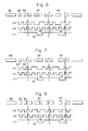
- Figs. 6 to 8 illustrate other forms of the clock track of the optical recording medium and waveforms of signals generated from clock reading circuits which correspond to said other forms of the clock track, respectively.
- Clock tracks 82, 84 and 86 of Figs. 6 to 8 have irregular clock bits 47, respectively, which are different from that of Fig.2.
- Waveforms (a) of the respective read clocks are also different from that of Fig. 1 accordingly.
- a common feature of the irregular clock bits 47 of the respective clock tracks shown in Figs.1, 6 to 8 is that a clock bit is provided at a position where no clock bit is formed in a clock track comprised only of regular, periodical clock bits 32. In other words, an optically changed state identical with those of the clock bits 32 is formed at a space between two clock bits 32 according to necessity. Therefore, although the waveforms (a) are different between Figs. 6 to 8, the resultant waveforms (c) are the same. More particularly, since the waveform of the read clock is at a "low" level at rising 72 of the output clock generated from the PLL circuit when the irregular bit is read, a detection pulse 70 is then generated.
- the present invention is suitably applied to a system in which a read word is stored in a storage means when the PLL circuit is being kept locked, but the read word is not stored when the PLL circuit is out of lock.
Landscapes
- Engineering & Computer Science (AREA)
- Signal Processing (AREA)
- Signal Processing For Digital Recording And Reproducing (AREA)
- Optical Recording Or Reproduction (AREA)
- Stabilization Of Oscillater, Synchronisation, Frequency Synthesizers (AREA)
Abstract
A circuit for reading from an optical recording medium having a clock track which is provided in parallel with data tracks and holds recorded clock bits forming a predetermined optical pattern. A reader circuit reads a clock track which contains a series of regularly arranged clock bits and some irregular clock bits that disturb the regularity of the former clock bits. This circuit includes a phase-locked loop (PLL) circuit for receiving the clock signal read from the clock track, and irregular clock detecting means for comparing the clock output of the PLL circuit with the read signal to generate a detect pulse when the disturbing irregular clock bit is detected. Even if the PLL circuit gets unlocked temporarily, the head word is recognized according to irregular clock bits provided in the clock track when the PLL circuit returns to the locked condition. Therefore, the data which are read subsequently can be properly recognized. Further, the invention can be realized without decreasing the recording capacity of the optical recording medium.
ABSTRACT
A reading circuit for an optical recording medium having a clock track having a predetermined optical pattern formed along data tracks and comprising at least one irregular clock bit disposed in a line formed of regular and periodical clock bits, breaking the regularity of the periodically arranged clock bits, which circuit comprises: a phase locked loop (PLL) circuit receiving read clocks obtained by reading the clock track; and an irregular clock detecting means comparing a clock output from the PLL circuit and the read signal and generating a detection pulse when it detects the irregular clock bit which breaks the regularity of the periodically arranged clock bits. According to the present invention, when the PLL circuit is reinstated into the locked position after the PLL circuit has fallen into the out-of-locked position, a leading word can be identified by the irregular clock bit provided in the clock track. Therefore, the read data thereafter can be recognized accurately. This can be attained without lowering the recording capacity of the optical recording medium.
Description
- This invention relates to a reading circuit for an optical recording medium having at least one clock track provided along a data track or tracks, in which the clock track has a predetermined optical pattern of clock bits formed thereon.
- Recently, an optical recording medium, which has a data recording surface having optically changed patterns, such as light and dark pits, formed thereon to represent digital data, has been attracting public attention. The optical recording medium could realize a memory of a large capacity because of its high density data recording capability. Thus, there has been contemplated, as an optical memory, not only a disc type memory but also a card type memory.
- In the card type optical memory or optical memory card, recording is made by forming optical (or magnetooptical) changes in response to data to be recorded at discrete spots on the surface thereof, and then a light beam, such as a laser beam, is projected thereonto to read the changes.
- More specifically, fine unevenness or light and dark patterns are provided on a surface of a recording medium or card. A light beam is projected onto such optical patterns to read the recorded data according to a difference in reflectivities, refractive indexes, or transmissivities between the optically changed states of the medium. Alternatively, the recording medium may have photothermo-magnetical record thereon and the recorded data may be read depending upon a change of polarization of the projected light due to the magnetooptical effect.
- In juxtaposition with each of the data tracks of the optical memory card, there are provided a clock track for synchronization in a data write/read operation and a tracking guide line as a reference for letting the optical beam from an optical reading system follow the track accurately.
- The write/read timing for the optical recording medium is conventionally determined by a clock signal derived by a detector dedicated for detecting clock bits of the clock track.
- Incidentally, if the clock is not accurately read in reading the clock track of the optical recording medium by reason of dust, scratch or the like on the optical recording medium or fluctuations of the moving velocity of the recording medium relative to the optical reading system, then it will be difficult to achieve accurate write/read operation. An absence of the clock during a short term or in relatively slow fluctuations of the velocity can be coped with by using a phase locked loop (PLL) circuit which produces a clock of a frequency synchronized with the input of the read out clock.
- Fig. 5 illustrates a typical arrangement of a prior art PLL circuit. The
PLL circuit 66 comprises aphase comparator 52, a low pass filter (LPF) 54, anamplifier 56, a voltage controlled oscillator (VCO) 58 and a 1/N frequency divider 53. This circuit compares, in phase, a received input signal with an output of thedivider 53 so as to match the phase through control of theVCO 58, thus producing, at the output thereof, a clock of a frequency of N times of that of the input signal. When N is 1, a VCO output fonformed with the frequency of the input signal will appear at the output terminal of thePLL circuit 66. - However, for a long-term absence of the clock or for an abrupt change of the relative moving velocity of the medium, the PLL circuit could not ensure the accurate data reading and it may fall into an out-of-locked state. In this case, the following problems may occur. When one data is formed of a plurality of words (a "word" used here means one bit or a plurality of bits to be read by one clock), if the PLL circuit gets unlocked or gets into an out-of-locked state, some words will not be read normally. In this state, if the PLL circuit is reinstated into the locked position again, it can in no way be identified which word in the data is being read.
- The present invention has been made to overcome the problems involved in the prior arts and it is an object of the present invention to provide a reading circuit for an optical recording medium which is capable of identifying a first word for a succeeding data when the PLL circuit is reinstated into the locked position after the PLL circuit has fallen into the out-of-locked position and some recorded words have failed to be read normally.
- The present invention features a reading circuit for a clock track having at least one irregular clock bit disposed in a line in which clock bits are regularly and periodically arranged, breaking the regularity of the periodically arranged clock bits, which circuit comprises, as illustrated in Fig. 2, a phase locked loop (PLL) circuit receiving read clocks obtained by reading the clock track and an irregular clock detecting means comparing a clock output from the PLL circuit with the read signal and generating a detection pulse when it detects the irregular clock bit which breaks the regularity of the periodically arranged clock bits.
- According to the present invention, the irregular clock bit is disposed in the line wherein the clock bits are arranged regularly, which enables information for the leading word of the data to be read from the optical recording medium without lowering the data recording density.
- With this arrangement, when the PLL circuit is reinstated into the locked position after the PLL circuit for the clocks has fallen into the out-of-locked position and the recorded word or words are not read normally, a first word for one data after the restoration of the PLL circuit into the locked position can be identified.
- The present invention is preferably employed for a system in which the out-of-locked state of the PLL circuit is detected to determine that the clock for data reading is not normal when the out-of-locked state is detected and inhibit address updating for a storage means which stores the read data, while allowing only normal data to be stored.
- As described above, with the reading circuit for the optical recording medium according to the present invention, when the PLL circuit is reinstated into the locked position after the PLL circuit has fallen into the out-of-locked position, a leading word can be identified by the irregular clock bit provided in the clock track. Therefore, the read data thereafter can be recognized accurately. This can be attained without lowering and recording capacity of the optical recording medium.
-
- Fig. 1 is a block diagram of a formation of a clock reading circuit for an optical recording medium according to the present invention;
- Fig. 2 is an explanatory view showing one form of an optical recording medium to which the present invention is to be applied;
- Fig. 3 is a block diagram of a specific arrangement of the clock reading circuit for the optical recording medium according to the present invention;
- Fig. 4 is a timing waveform diagram showing signal waveforms at essential portions of the circuit shown in Fig. 3;
- Fig. 5 is a diagram showing an arrangement of a conventional PLL circuit; and
- Fig. 6 to 8 are explanatory views each showing a modification of the clock track according to the present invention and a signal waveform corresponding thereto, respectively.
- Preferred embodiments of the present invention will now be described, referring to the attached drawings. First, a constitution of the optical recording medium to which the present invention is applied will be described. (Constitution of Optical Recording Medium)
- In an embodiment as illustrated, an optical memory card is contemplated as an example of an optical recording medium. However, the embodiment may also be applicable to another type of the optical recording medium. The optical memory card as illustrated is so formed that a plurality of data tracks are read simultaneously by each of clock bits. However, the present embodiment may also be applicable to the optical memory card in which only one data track is read by one clock bit.
- The optical memory card to which the present invention is applied comprises, as illustrated in Fig. 2, a
clock track 30 and adata track section 40 including a plurality ofdata lines 1 to n which are arranged along theclock track 30. Theclock track 30 is also used as a guide line for tracking in the present embodiment, but it may of course be provided separately from the guide line. - In the present specification, n bits formed of
data lines 1 to n which are read at one time by one clock bit are defined as one word. Theclock track 30 consists basically ofregular clock bits 32 which are arranged in line at equal intervals. Theclock track 30 further includesirregular clock bits 47 for leadingwords 46 of the respective data as described above. Each of theirregular clock bits 47 corressponds to the leadingword 46 and it is formed to continuously extend in length to a succeeding clock bit. Aword 48 may alternatively be used as a leading word. An interval A between the irregular clock bits is at least of a length of bits in which the PLL circuit can be maintained in a locked state. - Fig. 3 is a block diagram of one form of a clock reading circuit embodying the present invention. In the circuit as illustrated, a
delay element 67 and a D-flip-flop (hereinafter referred to as "D F/F") 68 are used for an irregular clock detecting means of Fig. 1. - A PLL circuit 66 (N = 1) receives a read clock which is a binary-coded signal changed from a read signal of the
clock track 30. D F/F 68 receives the read clock at its D input terminal and it receives, at its clock input terminal, anoutput 69 from thePLL circuit 69 through thedelay element 67 to generate a clock output at its Q output terminal. - In the case where a phase of the
output 69 from thePLL circuit 66 is delayed by a predetermined time from a phase of the read clock, there is no need to provide thedelay element 67. - An operation of the circuit shown in Fig. 3 will now be described, referring to a timing diagram of Fig. 4.
- The read clock input to the
PLL circuit 66 of Fig. 3 has a waveform as shown by (a) in Fig.4 in which one clock, periodical one, is missing in a term B. The term B corresponds to theirregular clock bit 47 of Fig. 2. If thePLL circuit 66 is in a locked state, the output from thecircuit 66 is a clock signal of a frequency conformed with a frequency of the input thereto. This clock signal is utilized as a clock signal for reading/writing of data. - On the other hand, the clock signal is delayed by the
delay element 67 to be a delayed clock signal (shown by (b) in Fig.4. D F/F 68 takes in the read clock (waveform (a)) by a leading edge of the delayed clock signal (waveform (b)). The delay time of thedelay element 67 is so determined that "high" levels of the read clocks may be taken in, except when the irregular clock bit is being read. Therefore, the Q output (waveform (c)) of D F/F 68 is normally kept "high", while the waveform (b) rises and the Q output of D F/F 68 becomes "low" if the waveform (a) becomes "low" during reading of the irregular clock bit (the term B). - When the waveform (b) rises again thereafter, the waveform (a) is reinstated into the "high" state and therefore the Q output is also reinstated into the "high" state. Thus, a
detection pulse 70 is output when the irregular clock bit is read. The leading word of the read data is identified in response to the detection pulse. (Other Forms of the Optical Recording Medium and Operation of the Reading Circuits) - Figs. 6 to 8 illustrate other forms of the clock track of the optical recording medium and waveforms of signals generated from clock reading circuits which correspond to said other forms of the clock track, respectively. Clock tracks 82, 84 and 86 of Figs. 6 to 8 have
irregular clock bits 47, respectively, which are different from that of Fig.2. Waveforms (a) of the respective read clocks are also different from that of Fig. 1 accordingly. - A common feature of the
irregular clock bits 47 of the respective clock tracks shown in Figs.1, 6 to 8 is that a clock bit is provided at a position where no clock bit is formed in a clock track comprised only of regular,periodical clock bits 32. In other words, an optically changed state identical with those of theclock bits 32 is formed at a space between twoclock bits 32 according to necessity. Therefore, although the waveforms (a) are different between Figs. 6 to 8, the resultant waveforms (c) are the same. More particularly, since the waveform of the read clock is at a "low" level at rising 72 of the output clock generated from the PLL circuit when the irregular bit is read, adetection pulse 70 is then generated. - The present invention is suitably applied to a system in which a read word is stored in a storage means when the PLL circuit is being kept locked, but the read word is not stored when the PLL circuit is out of lock.
- While a few embodiments of the invention have been illustrated and described in detail, various changes and modifications may be introduced without departing from the scope of the present invention. For example, the "high" and "low" of the respective waveforms of Fig.4 may be vice versa.
Claims (3)
- (1) A reading circuit for an optical recording medium having a clock track comprising at least one irregular clock bit disposed in a line formed of regular and periodical clock bits, breaking the regularity of the periodically arranged clock bits, which circuit comprises:
a phase locked loop (PLL) circuit receiving read clocks obtained by reading the clock track; and
an irregular clock detecting means comparing a clock output from the PLL circuit and the read signal and generating a detection pulse when it detects the irregular clock bit which breaks the regularity of the periodically arranged clock bits. - (2) A reading circuit for the optical recording medium as claimed in claim 1, wherein said irregular clock detecting means comprises a flip flop and a delay element.
- (3) A reading circuit for the optical recording medium as claimed in claim 1, wherein said flip flop comprises a D-type flip flop, said D-type flip flop being adapted to receive the read clock at its D-input terminal, said D-type flip flop being adapted to receive, at its clock input, an output from the PLL circuit, through the delay element.
Applications Claiming Priority (3)
| Application Number | Priority Date | Filing Date | Title |
|---|---|---|---|
| JP62168015A JPS6413267A (en) | 1987-07-06 | 1987-07-06 | Read circuit for optical recording medium |
| JP168015/87 | 1987-07-06 | ||
| CA000587290A CA1322248C (en) | 1987-07-06 | 1988-12-29 | Reading circuit for optical recording medium |
Publications (1)
| Publication Number | Publication Date |
|---|---|
| EP0321587A1 true EP0321587A1 (en) | 1989-06-28 |
Family
ID=25672341
Family Applications (1)
| Application Number | Title | Priority Date | Filing Date |
|---|---|---|---|
| EP88906072A Withdrawn EP0321587A1 (en) | 1987-07-06 | 1988-07-06 | Reader circuit for optical recording medium |
Country Status (4)
| Country | Link |
|---|---|
| EP (1) | EP0321587A1 (en) |
| JP (1) | JPS6413267A (en) |
| CA (1) | CA1322248C (en) |
| WO (1) | WO1989000330A1 (en) |
Family Cites Families (1)
| Publication number | Priority date | Publication date | Assignee | Title |
|---|---|---|---|---|
| JPS5479017A (en) * | 1977-12-07 | 1979-06-23 | Hitachi Ltd | Sector clock generating system |
-
1987
- 1987-07-06 JP JP62168015A patent/JPS6413267A/en active Pending
-
1988
- 1988-07-06 EP EP88906072A patent/EP0321587A1/en not_active Withdrawn
- 1988-07-06 WO PCT/JP1988/000679 patent/WO1989000330A1/en not_active Ceased
- 1988-12-29 CA CA000587290A patent/CA1322248C/en not_active Expired - Fee Related
Non-Patent Citations (1)
| Title |
|---|
| See references of WO8900330A1 * |
Also Published As
| Publication number | Publication date |
|---|---|
| JPS6413267A (en) | 1989-01-18 |
| WO1989000330A1 (en) | 1989-01-12 |
| CA1322248C (en) | 1993-09-14 |
Similar Documents
| Publication | Publication Date | Title |
|---|---|---|
| KR0132674B1 (en) | Optically readable recording media, apparatus for manufacturing same, and recording and reading devices | |
| JP2845915B2 (en) | Information reproducing method and information reproducing apparatus | |
| US4566092A (en) | Process and device for generating synchronizing signals in an optical data carrier write-read apparatus | |
| US4949325A (en) | Method and associated apparatus and medium for optical recording and reproducing information | |
| US4583208A (en) | Sector mark decoder for an optical recorder | |
| GB2097560A (en) | Apparatus for reproducing a pulse code modulated signal | |
| US4390910A (en) | Phase-lock oscillator | |
| KR0136098B1 (en) | Continuous recording method of EFM modulated signal and apparatus | |
| US7016284B2 (en) | Method and related circuit for generating a wobble clock and an ATIP clock through a reference clock and a wobble signal | |
| US5231650A (en) | Digital signal reproducing apparatus | |
| US5142524A (en) | Optical recording medium | |
| EP0321587A1 (en) | Reader circuit for optical recording medium | |
| US6961293B2 (en) | Method and related device for achieving stable writing state of compact disk drive by adjusting writing clock | |
| US5276667A (en) | Optical recording and reproducing apparatus for synchronizing recording on subsequent unrecorded sectors | |
| US4331985A (en) | Splicing-point detection apparatus and method | |
| EP0023783A1 (en) | Data recovery circuit | |
| EP0384405B1 (en) | Optical recording and reproducing apparatus | |
| JPS62139179A (en) | Synchronous control system | |
| JP3352132B2 (en) | Optical information reproducing device | |
| US5138597A (en) | Apparatus for detecting a read error of an optical recording medium | |
| US6272102B1 (en) | Amplitude detector for signals having a periodical character, recorded on a recording medium, and optical tape recorder comprising such an amplitude detector | |
| US5237550A (en) | Reloadable optical recording/reproducing apparatus | |
| JP2882611B2 (en) | Write-once optical recording / reproducing device | |
| JPH0580070B2 (en) | ||
| JPH04356730A (en) | Device and method for optical recording and reproduction |
Legal Events
| Date | Code | Title | Description |
|---|---|---|---|
| PUAI | Public reference made under article 153(3) epc to a published international application that has entered the european phase |
Free format text: ORIGINAL CODE: 0009012 |
|
| AK | Designated contracting states |
Kind code of ref document: A1 Designated state(s): DE FR GB IT |
|
| RBV | Designated contracting states (corrected) |
Designated state(s): DE FR GB |
|
| STAA | Information on the status of an ep patent application or granted ep patent |
Free format text: STATUS: THE APPLICATION IS DEEMED TO BE WITHDRAWN |
|
| 18D | Application deemed to be withdrawn |
Effective date: 19890713 |