EP0321801A1 - Thyristor à extinction comportant une protection contre les surtensions - Google Patents
Thyristor à extinction comportant une protection contre les surtensions Download PDFInfo
- Publication number
- EP0321801A1 EP0321801A1 EP88120593A EP88120593A EP0321801A1 EP 0321801 A1 EP0321801 A1 EP 0321801A1 EP 88120593 A EP88120593 A EP 88120593A EP 88120593 A EP88120593 A EP 88120593A EP 0321801 A1 EP0321801 A1 EP 0321801A1
- Authority
- EP
- European Patent Office
- Prior art keywords
- zone
- fet
- anode
- gate
- cathode
- Prior art date
- Legal status (The legal status is an assumption and is not a legal conclusion. Google has not performed a legal analysis and makes no representation as to the accuracy of the status listed.)
- Granted
Links
- 230000004224 protection Effects 0.000 title claims abstract description 21
- 239000000758 substrate Substances 0.000 claims description 15
- 238000001465 metallisation Methods 0.000 claims description 3
- 238000000926 separation method Methods 0.000 abstract description 2
- 239000003990 capacitor Substances 0.000 description 4
- 238000001816 cooling Methods 0.000 description 4
- 238000006073 displacement reaction Methods 0.000 description 3
- 230000003321 amplification Effects 0.000 description 2
- 238000001514 detection method Methods 0.000 description 2
- 230000010354 integration Effects 0.000 description 2
- 238000003199 nucleic acid amplification method Methods 0.000 description 2
- 230000015572 biosynthetic process Effects 0.000 description 1
- 230000015556 catabolic process Effects 0.000 description 1
- 239000000919 ceramic Substances 0.000 description 1
- 238000009795 derivation Methods 0.000 description 1
- 238000005538 encapsulation Methods 0.000 description 1
- 230000005669 field effect Effects 0.000 description 1
- 238000004519 manufacturing process Methods 0.000 description 1
- 230000009979 protective mechanism Effects 0.000 description 1
- 239000004065 semiconductor Substances 0.000 description 1
- 230000035945 sensitivity Effects 0.000 description 1
- 229910052710 silicon Inorganic materials 0.000 description 1
- 239000010703 silicon Substances 0.000 description 1
- 238000009827 uniform distribution Methods 0.000 description 1
Images

Classifications
-
- H—ELECTRICITY
- H03—ELECTRONIC CIRCUITRY
- H03K—PULSE TECHNIQUE
- H03K17/00—Electronic switching or gating, i.e. not by contact-making and –breaking
- H03K17/08—Modifications for protecting switching circuit against overcurrent or overvoltage
- H03K17/082—Modifications for protecting switching circuit against overcurrent or overvoltage by feedback from the output to the control circuit
- H03K17/0824—Modifications for protecting switching circuit against overcurrent or overvoltage by feedback from the output to the control circuit in thyristor switches
Definitions
- the present invention relates to the field of power semiconductors. It relates in particular to a thyristor that can be switched off with overvoltage protection, in particular for use in a series connection of several thyristors, which thyristor that can be switched off has an anode, a cathode and a gate.
- the thyristors are therefore connected in series. This is possible because you can master the necessary uniform distribution of the total voltage between the individual elements by simultaneous ignition and a suitable additional circuit.
- Such an additional circuit for conventional thyristors is known, for example, from SCR Manual, 5th Edition (1972) from General Electric, pp. 156-159. On the one hand, it can be designed as a so-called “snubber” circuit composed of passive elements such as resistors and capacitors (FIG. 6.7 there).
- it can also include active elements such as varistors or avalanche diodes (Fig. 6.9), which become conductive above a critical voltage and thus represent active overvoltage protection.
- active elements such as varistors or avalanche diodes (Fig. 6.9), which become conductive above a critical voltage and thus represent active overvoltage protection.
- EP-A2 0209 986 it is also known (EP-A2 0209 986) to provide an avalanche zone in the case of a conventional thyristor with an “amplifying gate” as overvoltage protection within the substrate, said zone being controlled at a critical voltage and switching on the thyristor part via its gate.
- the disadvantage here is that the thyristor itself is used to reduce the overvoltage, so there is no protective mechanism independent of the thyristor.
- GTOs and FCThs are said to operate at a relatively high frequency. Because of the storage time specific to these thyristors, their switch-off time depends heavily on the control. At the same time, the size of the storage charge differs at least as much for the individual elements as for conventional thyristors. The consequence of this is that a corresponding snubber circuit would have to be very powerful, which would lead to a disproportionately high power loss.
- thyristors that can be switched off only have active overvoltage protection in the form of an arrester (varistor or avalanche diode) in question.
- an arrester variant or avalanche diode
- such arresters must be designed for quite high outputs: at 4 kV clamping voltage, 1000 A switch-off current, 2 kHz repetition frequency and 0.3 microsecond loading of the arrester per period, there is a power loss of 2.4 kW per arrester .
- ZnO varistors too, cannot dissipate much more than 200 W of power due to their low thermal conductivity (the ceramic), the encapsulation and cooling of such elements being about as complex as that of high-performance thyristors.
- the object of the present invention is to provide a thyristor that can be switched off and has overvoltage protection, which requires comparatively little additional effort and can be implemented using known means.
- the problem is solved in a thyristor of the type mentioned above that -
- the overvoltage protection comprises a controllable resistor and an overvoltage sensor;
- the controllable resistor is connected to the turn-off thyristor in parallel between its anode and its cathode, and - Is controlled by the overvoltage sensor.
- the essence of the invention is therefore not to use a single heavy-duty component for overvoltage detection and voltage limitation, but to carry out the overvoltage detection with an overvoltage sensor of lower load capacity and to control a more resilient, controllable resistance with this sensor, which can be optimally adapted to the requirements.
- the thyristor that can be switched off is an FCTh
- the controllable resistor is a J-FET
- both are integrated next to one another on a common substrate.
- the overvoltage sensor can be a varistor or an avalanche diode, which can also be integrated into the substrate.
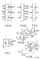
- the invention takes a completely different route: the switchable thyristor AT is connected in parallel between its anode A1 and its cathode K1 (FIG. 2), which is operated by an overvoltage sensor OS is controlled.
- the overvoltage sensor OS detects the overvoltage condition on the thyristor AT which can be switched off and then controls the controllable resistor in such a way that the overvoltage is reduced via it.
- controllable resistor is a J-FET (JF), the source S of which is connected to the cathode K1 and the drain D of which is connected to the anode A1 of the turn-off thyristor AT.
- JF J-FET
- controllable resistance can be optimally designed for the dissipated power dissipation.
- the controllable resistor in the form of a J-FET can be integrated directly with the thyristor on a common substrate, the same manufacturing technology and geometry being able to be used for both components (FIG. 4).
- Such an integrated avalanche zone would have to have an area larger than 5 cm2 in order to be able to dissipate the power loss in the range of several kW.
- a large area requires an unattainable homogeneity of the electrical properties in the avalanche zone, so that not only a few points in the zone take over the entire leakage current.
- FIG. 3A A first exemplary embodiment of a complete thyristor stage with drive circuit and overvoltage protection according to the invention is shown in FIG. 3A.
- a cascade circuit comprising the switchable thyristor AT and an auxiliary thyristor HT is provided on the control side. Both thyristors are FCThs.
- the drive circuit further comprises a capacitor C, a series resistor RV1 and a voltage source VS.
- a gate voltage V G1 is present at the capacitor C; the auxiliary thyristor is driven by an input signal V IN .
- FCThs are thyristors that are conductive in the event of a short circuit between the gate and cathode (so-called "normally-ON" components)
- the voltage source VS is eliminated;
- the series resistor RV1 is then directly on the cathode K1.
- the voltage source VS has a voltage of approximately 5 V.
- the overvoltage protection of the thyristor stage comprises the parallel-connected J-FET JF, a varistor V (or an avalanche diode AD) as an overvoltage sensor, and a gate resistor RG.
- the varistor V is connected between the gate G2 and the drain D of the J-FET and has e.g. a kink voltage of 4 kV.
- the gate resistor RG connects the gate G2 to the gate G1 of the turn-off thyristor AT. This has the special advantage that simple integration of the overvoltage protection is possible.
- the varistor V in the circuit according to FIG. 3A still carries a relatively high part of the total power loss and must therefore be chosen to be correspondingly large.
- an additional amplification stage is therefore provided between the varistor V and the J-FET in a second exemplary embodiment (FIG. 3B), which in the example comprises a transistor T and a second series resistor RV2.
- the varistor V can be designed at least 10 times smaller.
- the transistor T is otherwise supplied by the same voltage source VS as the thyristor cascade HT, AT.
- FCTh as the thyristor AT which can be switched off and to integrate it with the J-FET on a common substrate according to FIG. 4 (possibly together with an avalanche zone as an overvoltage sensor).
- the 2.4 kW average power assumed at the beginning would mean a power loss of 500 W / cm2, which is also at the upper limit even with very good cooling. Since a corresponding GTO thyristor or FCTh requires an area of at least 20 cm2 anyway, the area of the J-FET can be increased somewhat without difficulty.
- a varistor e.g. the series connection of two varistors of the type SIOV-S14K680 and SIOV-S14K1000 from Siemens in question.
- the voltage at 1A is then about 4 kV, the capacitance 80 pF.
- the varistors at a repetition frequency of 2 kHz and a load of 0.3 microseconds per period result in a power loss of 9.6 W, which can be easily dissipated by direct cooling.
- FCTh and J-FET (and in addition an avalanche zone or diode) will now be explained using the exemplary embodiment in FIG. 4, in which a corresponding substrate is shown in sections in cross section.
- the substrate is laterally divided into three areas.
- the FCTh structure is arranged in the left area, the J-FET structure in the middle area, and the avalanche diode structure (AD) in the right area.
- AD avalanche diode structure
- the FCTh structure is of the "recessed gate” type with a step-shaped gate-cathode structure which has a plurality of control fingers 9 separated by trenches.
- Such an FCTh is e.g. known from EP-A2 0 178 387.
- the FCTh structure comprises between the anode A1 and the cathode K1 a layer sequence of a p+-doped anode zone 7, an n ⁇ -doped channel layer 5, a p-doped gate zone 4 and n+-doped cathode regions 2.
- the cathode regions 2 are arranged on the top of the control fingers 9.
- the channel layer 5 extends into this control finger 9 and borders there on the cathode regions 2.
- the gate zone 4 extends in each case over the bottoms and walls of the trenches and, together with the channel layer 5 running in the control finger, forms a long channel which can be controlled by a field effect.
- the gate zone 4 is provided on the trench floors with gate contacts 3, the cathode regions 2 on the control fingers 9 with corresponding cathode contacts 1.
- a large-area anode contact 8 establishes the electrical connection to the anode zone 7.
- the structure and geometry of the J-FET structure in the central region of the substrate is comparable to that of the neighboring FCTh structure, with the difference that here a n-doped drain zone 15 takes the place of the p-doped anode zone 7.
- n-doped buffer layer 6 which runs below the channel layers 5, 14 and separates the anode zone 7 and drain zone 15 from one another and from these channel layers.
- the drain D of the J-FET is connected to the anode A1 of the FCTh.
- the cathode contacts 1 and the source contacts 10 can be brought together to form a common connection.
- the J-FET then lies with its source S on the cathode K1 of the FCTh.
- the gate G2 of the J-FET lies above the gate resistor RG at the gate G1 of the FCTh.
- This gate resistance RG is expediently realized in that the gate contacts 3 and 12 of the FCTh or J-FET, which are on the same level, are not designed as a continuous metallization layer, but instead have a gap between them with a correspondingly selected distance d. The part of the gate zone 4, 13 below this gap then forms the desired gate resistance RG.
- an avalanche diode AD is provided as an overvoltage sensor instead of an external varistor V, this diode can also be integrated into the substrate in the form of an avalanche zone, as shown in FIG. 4 (right area).
- the diode structure comprises a sequence of four zones 18, 19, 20 and 21.
- the first zone 18 is p+-doped and a continuation of the gate zone 13 of the adjacent J-FET.
- the second zone 19 is n ⁇ -doped and a continuation of the channel layer 14, but with a reduced thickness in order to achieve suitable breakdown voltages.
- the third zone 20 is n-doped and a direct continuation of the buffer layer 6.
- the fourth zone 21 is n+-doped and is a direct continuation of the drain zone 15.
- Both the anode contact 17 and the cathode contact 22 are respectively continuations of the gate contact 12 and the drain contact 16.
- FCTh FCTh
- J-FET J-FET
- AD AD
- the disconnectable thyristor according to the invention provides a component that is protected against overvoltages and that can be implemented with little effort, compactly constructed and easily integrated.
Landscapes
- Thyristors (AREA)
- Junction Field-Effect Transistors (AREA)
Applications Claiming Priority (2)
| Application Number | Priority Date | Filing Date | Title |
|---|---|---|---|
| CH5014/87 | 1987-12-23 | ||
| CH501487 | 1987-12-23 |
Publications (2)
| Publication Number | Publication Date |
|---|---|
| EP0321801A1 true EP0321801A1 (fr) | 1989-06-28 |
| EP0321801B1 EP0321801B1 (fr) | 1992-04-01 |
Family
ID=4286455
Family Applications (1)
| Application Number | Title | Priority Date | Filing Date |
|---|---|---|---|
| EP88120593A Expired - Lifetime EP0321801B1 (fr) | 1987-12-23 | 1988-12-09 | Thyristor à extinction comportant une protection contre les surtensions |
Country Status (4)
| Country | Link |
|---|---|
| US (1) | US4885657A (fr) |
| EP (1) | EP0321801B1 (fr) |
| JP (1) | JP2622524B2 (fr) |
| DE (1) | DE3869752D1 (fr) |
Cited By (3)
| Publication number | Priority date | Publication date | Assignee | Title |
|---|---|---|---|---|
| DE19854821A1 (de) * | 1998-11-27 | 2000-05-31 | Bosch Gmbh Robert | Schutzschaltung für eine getaktete Halbleiter-Endstufe |
| DE19710484C2 (de) * | 1996-03-13 | 2001-07-19 | Omron Tateisi Electronics Co | Kontaktloses Relais |
| DE102006046040A1 (de) * | 2006-09-28 | 2008-04-03 | Siemens Ag | Thyristorventil einer HGÜ-Anlage |
Families Citing this family (8)
| Publication number | Priority date | Publication date | Assignee | Title |
|---|---|---|---|---|
| JPH0821840B2 (ja) * | 1989-12-07 | 1996-03-04 | 富士電機株式会社 | パワー半導体装置のスナバ回路 |
| DE19523096A1 (de) * | 1995-06-26 | 1997-01-02 | Abb Management Ag | Stromrichterschaltungsanordnung |
| US6169672B1 (en) * | 1996-07-03 | 2001-01-02 | Hitachi, Ltd. | Power converter with clamping circuit |
| JP2000012780A (ja) * | 1998-06-26 | 2000-01-14 | Toshiba Corp | 半導体スナバ装置及び半導体装置 |
| JP4675302B2 (ja) * | 2006-09-25 | 2011-04-20 | 三菱電機株式会社 | 半導体装置 |
| GB0810123D0 (en) * | 2008-06-03 | 2008-07-09 | Smarter Energy Holdings Ltd | Electricity control device |
| CN101505057B (zh) * | 2009-03-20 | 2011-05-25 | 中国电力科学研究院 | 串联功率器件均压保护方法、功率器件和避雷器阀开关 |
| EP3200331B1 (fr) | 2016-01-27 | 2019-11-20 | GE Energy Power Conversion Technology Ltd | Procédé pour protéger un agencement de convertisseur de puissance et agencement de convertisseur de puissance avec un dispositif de protection |
Citations (3)
| Publication number | Priority date | Publication date | Assignee | Title |
|---|---|---|---|---|
| DE3425414A1 (de) * | 1984-07-10 | 1986-01-16 | Siemens AG, 1000 Berlin und 8000 München | Leistungsschalter mit einem abschaltthyristor |
| DE3537419A1 (de) * | 1985-10-21 | 1987-04-23 | Siemens Ag | Schaltungsanordnung zum schutz eines lichtsteuerbaren thyristors |
| EP0224757A1 (fr) * | 1985-11-29 | 1987-06-10 | BBC Brown Boveri AG | Thyristor à conduction inverse |
Family Cites Families (8)
| Publication number | Priority date | Publication date | Assignee | Title |
|---|---|---|---|---|
| FR2446026A1 (fr) * | 1979-01-05 | 1980-08-01 | Paris & Du Rhone | Dispositif de protection contre les surtensions |
| US4319318A (en) * | 1980-09-15 | 1982-03-09 | California Institute Of Technology | Voltage reapplication rate control for commutation of thyristors |
| DE3112941A1 (de) * | 1981-03-31 | 1982-10-07 | Siemens AG, 1000 Berlin und 8000 München | Thyristor mit innerer stromverstaerkung und verfahren zu seinem betrieb |
| DE3586735D1 (de) * | 1984-10-19 | 1992-11-12 | Bbc Brown Boveri & Cie | Abschaltbares leistungshalbleiterbauelement. |
| JPS61221528A (ja) * | 1985-03-25 | 1986-10-01 | 三菱電機株式会社 | ゲ−トタ−ンオフサイリスタのスナバ回路 |
| IE861474L (en) * | 1985-06-20 | 1986-12-20 | Tsnii Kozhevenno Obuvnoi Ptomy | Temperature stable self-protected thyristor and method of¹producing |
| EP0219995B1 (fr) * | 1985-09-30 | 1994-03-02 | Kabushiki Kaisha Toshiba | Thyristor à commande d'extinction comportant des transistors d'allumage/extinction indépendants |
| EP0246478A1 (fr) * | 1986-05-22 | 1987-11-25 | BBC Brown Boveri AG | Interrupteur de puissance à semi-conducteur |
-
1988
- 1988-12-09 EP EP88120593A patent/EP0321801B1/fr not_active Expired - Lifetime
- 1988-12-09 DE DE8888120593T patent/DE3869752D1/de not_active Expired - Lifetime
- 1988-12-22 US US07/288,272 patent/US4885657A/en not_active Expired - Fee Related
- 1988-12-23 JP JP63325721A patent/JP2622524B2/ja not_active Expired - Lifetime
Patent Citations (3)
| Publication number | Priority date | Publication date | Assignee | Title |
|---|---|---|---|---|
| DE3425414A1 (de) * | 1984-07-10 | 1986-01-16 | Siemens AG, 1000 Berlin und 8000 München | Leistungsschalter mit einem abschaltthyristor |
| DE3537419A1 (de) * | 1985-10-21 | 1987-04-23 | Siemens Ag | Schaltungsanordnung zum schutz eines lichtsteuerbaren thyristors |
| EP0224757A1 (fr) * | 1985-11-29 | 1987-06-10 | BBC Brown Boveri AG | Thyristor à conduction inverse |
Cited By (4)
| Publication number | Priority date | Publication date | Assignee | Title |
|---|---|---|---|---|
| DE19710484C2 (de) * | 1996-03-13 | 2001-07-19 | Omron Tateisi Electronics Co | Kontaktloses Relais |
| DE19854821A1 (de) * | 1998-11-27 | 2000-05-31 | Bosch Gmbh Robert | Schutzschaltung für eine getaktete Halbleiter-Endstufe |
| DE19854821B4 (de) * | 1998-11-27 | 2004-07-29 | Robert Bosch Gmbh | Schutzschaltung für eine getaktete Halbleiter-Endstufe |
| DE102006046040A1 (de) * | 2006-09-28 | 2008-04-03 | Siemens Ag | Thyristorventil einer HGÜ-Anlage |
Also Published As
| Publication number | Publication date |
|---|---|
| JP2622524B2 (ja) | 1997-06-18 |
| DE3869752D1 (de) | 1992-05-07 |
| US4885657A (en) | 1989-12-05 |
| EP0321801B1 (fr) | 1992-04-01 |
| JPH01280355A (ja) | 1989-11-10 |
Similar Documents
| Publication | Publication Date | Title |
|---|---|---|
| DE3011484C2 (de) | Optisch steuerbare Halbleitervorrichtung | |
| DE60028850T2 (de) | Bipolartransistor mit isoliertem Gate | |
| DE19811297B4 (de) | MOS-Halbleitervorrichtung mit hoher Durchbruchspannung | |
| DE2625917C3 (de) | Halbleiteranordnung | |
| DE3047738C2 (de) | Halbleiteranordnung | |
| DE10250575B4 (de) | IGBT mit monolithisch integrierter antiparalleler Diode | |
| DE2257846B2 (de) | Integrierte Halbleiteranordnung zum Schutz gegen Überspannung | |
| EP1320133A2 (fr) | IGBT avec grille dans une tranchée | |
| DE69225026T2 (de) | Überspannungsgeschützter Halbleiterschalter | |
| DE69302244T2 (de) | Halbleiter-Schutzkomponente | |
| DE68923789T2 (de) | Optische halbleitervorrichtung mit einer nulldurchgangsfunktion. | |
| EP0321801B1 (fr) | Thyristor à extinction comportant une protection contre les surtensions | |
| DE3018468A1 (de) | Thyristor mit steuerbaren emitterkurzschluessen und verfahren zu seinem betrieb | |
| EP0507974B1 (fr) | Dispositif semi-conducteur de puissance, ouvrable, à commande de type MOS | |
| EP1097482A1 (fr) | Ensemble a semi-conducteur, en particulier transistor a effet de champ a jonction | |
| DE3540433A1 (de) | Integriertes mosfet-bauelement | |
| DE2906961A1 (de) | Feldgesteuerte thyristor-steueranordnung | |
| EP1284019A2 (fr) | Composant semi-conducteur de puissance | |
| EP0487869B1 (fr) | Dispositif semi-conducteur de puissance, à extinction | |
| EP0742957B1 (fr) | Thyristor a commande mos | |
| EP0249122A1 (fr) | Dispositif semi-conducteur de puissance pouvant être mis hors circuit | |
| EP0344514A2 (fr) | Thyristor à commande d'extinction | |
| WO2000033380A1 (fr) | Element a semiconducteur pouvant etre commande, comprenant une resistance de grille en serie | |
| DE69318346T2 (de) | Schutzdiode für ein vertikales Halbleiterbauelement | |
| DE2929869A1 (de) | Monolithisch integrierte cmos-schaltung |
Legal Events
| Date | Code | Title | Description |
|---|---|---|---|
| PUAI | Public reference made under article 153(3) epc to a published international application that has entered the european phase |
Free format text: ORIGINAL CODE: 0009012 |
|
| AK | Designated contracting states |
Kind code of ref document: A1 Designated state(s): CH DE FR GB IT LI NL SE |
|
| 17P | Request for examination filed |
Effective date: 19891211 |
|
| 17Q | First examination report despatched |
Effective date: 19910124 |
|
| GRAA | (expected) grant |
Free format text: ORIGINAL CODE: 0009210 |
|
| AK | Designated contracting states |
Kind code of ref document: B1 Designated state(s): CH DE FR GB IT LI NL SE |
|
| PG25 | Lapsed in a contracting state [announced via postgrant information from national office to epo] |
Ref country code: NL Effective date: 19920401 |
|
| REF | Corresponds to: |
Ref document number: 3869752 Country of ref document: DE Date of ref document: 19920507 |
|
| ITF | It: translation for a ep patent filed | ||
| ET | Fr: translation filed | ||
| GBT | Gb: translation of ep patent filed (gb section 77(6)(a)/1977) | ||
| NLV1 | Nl: lapsed or annulled due to failure to fulfill the requirements of art. 29p and 29m of the patents act | ||
| PGFP | Annual fee paid to national office [announced via postgrant information from national office to epo] |
Ref country code: SE Payment date: 19921123 Year of fee payment: 5 |
|
| PG25 | Lapsed in a contracting state [announced via postgrant information from national office to epo] |
Ref country code: LI Effective date: 19921231 Ref country code: CH Effective date: 19921231 |
|
| PLBE | No opposition filed within time limit |
Free format text: ORIGINAL CODE: 0009261 |
|
| STAA | Information on the status of an ep patent application or granted ep patent |
Free format text: STATUS: NO OPPOSITION FILED WITHIN TIME LIMIT |
|
| 26N | No opposition filed | ||
| REG | Reference to a national code |
Ref country code: CH Ref legal event code: PL |
|
| PG25 | Lapsed in a contracting state [announced via postgrant information from national office to epo] |
Ref country code: SE Effective date: 19931210 |
|
| EUG | Se: european patent has lapsed |
Ref document number: 88120593.4 Effective date: 19940710 |
|
| PGFP | Annual fee paid to national office [announced via postgrant information from national office to epo] |
Ref country code: GB Payment date: 19991112 Year of fee payment: 12 |
|
| PGFP | Annual fee paid to national office [announced via postgrant information from national office to epo] |
Ref country code: FR Payment date: 19991123 Year of fee payment: 12 Ref country code: DE Payment date: 19991123 Year of fee payment: 12 |
|
| PG25 | Lapsed in a contracting state [announced via postgrant information from national office to epo] |
Ref country code: GB Free format text: LAPSE BECAUSE OF NON-PAYMENT OF DUE FEES Effective date: 20001209 |
|
| GBPC | Gb: european patent ceased through non-payment of renewal fee |
Effective date: 20001209 |
|
| PG25 | Lapsed in a contracting state [announced via postgrant information from national office to epo] |
Ref country code: FR Free format text: LAPSE BECAUSE OF NON-PAYMENT OF DUE FEES Effective date: 20010831 |
|
| REG | Reference to a national code |
Ref country code: FR Ref legal event code: ST |
|
| PG25 | Lapsed in a contracting state [announced via postgrant information from national office to epo] |
Ref country code: DE Free format text: LAPSE BECAUSE OF NON-PAYMENT OF DUE FEES Effective date: 20011002 |
|
| PG25 | Lapsed in a contracting state [announced via postgrant information from national office to epo] |
Ref country code: IT Free format text: LAPSE BECAUSE OF NON-PAYMENT OF DUE FEES;WARNING: LAPSES OF ITALIAN PATENTS WITH EFFECTIVE DATE BEFORE 2007 MAY HAVE OCCURRED AT ANY TIME BEFORE 2007. THE CORRECT EFFECTIVE DATE MAY BE DIFFERENT FROM THE ONE RECORDED. Effective date: 20051209 |