EP0322025B1 - Circuit d'émission - Google Patents
Circuit d'émission Download PDFInfo
- Publication number
- EP0322025B1 EP0322025B1 EP88202851A EP88202851A EP0322025B1 EP 0322025 B1 EP0322025 B1 EP 0322025B1 EP 88202851 A EP88202851 A EP 88202851A EP 88202851 A EP88202851 A EP 88202851A EP 0322025 B1 EP0322025 B1 EP 0322025B1
- Authority
- EP
- European Patent Office
- Prior art keywords
- coupled
- transmitter circuit
- terminal
- terminals
- output
- Prior art date
- Legal status (The legal status is an assumption and is not a legal conclusion. Google has not performed a legal analysis and makes no representation as to the accuracy of the status listed.)
- Expired - Lifetime
Links
- 230000005540 biological transmission Effects 0.000 claims description 16
- 238000004804 winding Methods 0.000 description 4
- 230000000694 effects Effects 0.000 description 2
- 230000005669 field effect Effects 0.000 description 2
- 230000007423 decrease Effects 0.000 description 1
- 238000010586 diagram Methods 0.000 description 1
- 230000001105 regulatory effect Effects 0.000 description 1
Images

Classifications
-
- H—ELECTRICITY
- H04—ELECTRIC COMMUNICATION TECHNIQUE
- H04L—TRANSMISSION OF DIGITAL INFORMATION, e.g. TELEGRAPHIC COMMUNICATION
- H04L25/00—Baseband systems
- H04L25/02—Details ; arrangements for supplying electrical power along data transmission lines
Definitions
- the present invention relates to a transmitter circuit for a transmission system wherein a plurality of such transmitter circuits are coupled in parallel to a transmission line which is coupled to a receiver circuit, said transmitter circuit having an output which is electrically coupled to said line but is galvanically isolated therefrom and is able to supply at said output a current and to limit this current in function of the voltage on said output.
- the transmitter circuits and the receiver circuit form part of respective S-interface circuits located in subscriber stations and in a network station respectively, this network station being coupled to a digital exchange through a subscriber line.
- Each of these S-interface circuits further includes a receiver circuit and a transmitter circuit respectively, these receiver circuits being coupled in parallel to another transmission line to which the transmitter circuit of the network station has access.
- the S-interface circuits are for instance of the type disclosed in the article "ISDN Components for Public and Private Digital Loops" by P. Van Iseghem et al, Electrical Communication, Volume 61, November 1, 1987, pp 63-71.
- Each S-interface circuit is for instance able to transmit a 192 kbit/sec signal consisting of groups of frames of 42 bits, 36 of which are information bits part of two B channels of 16 bits each and of a D channel of 4 bits. Thus 12 bits per frame are left for signals which may be added by the interface.
- four of these bits form an echo channel for the retransmission of the D channel bits received from the subscriber station. This retransmission is required to ensure that only one transmitter circuit makes use of this channel. Indeed, the transmitter circuit of a subscriber station starts transmitting the address assigned to this station only when the D channel is free.
- this station When the bits of this address are received in the network station receiver they are retransmitted to the subscriber station receiver with a predetermined delay in the D echo channels, and the transmitter of this station only transmits a next bit after it has received the echo bits. As long as these bits are the same as the transmitted D channel bits the subscriber station transmitter continues transmitting. However, if in this station a difference is detected due to several subscriber station transmitter circuits having simultaneously transmitted their addresses this station ceases transmission.
- a pseudoternary code in which a binary one is represented by the absence of current and binary zero by a positive and a negative current alternately.
- An object of the present invention is to provide a transmitter circuit of this type, but which is able to fulfill these requirements in a simple way.
- this object is achieved due to the fact that said transmitter output is shunted by a variable impedance which is controlled by the output of a servo control circuit which is operated in function of the difference between a reference voltage and a feedback voltage which is itself function of the transmitter circuit output voltage.
- the servo control circuit becomes operative for instance as soon as the feedback voltage decreases below the reference voltage and this feedback voltage is limited to the reference voltage due to which the output voltage of the transmitter circuit is limited.
- said servo control circuit includes a comparator circuit which is constituted by a first operational amplifier whose first and second inputs are controlled by said reference voltage and by said feedback voltage respectively.
- variable impedance is coupled, in series with a current source, across two DC supply voltages and that the end of said impedance which is connected to said current source is coupled to said second input of said first operational amplifier.
- the transmitter circuit output voltage is limited to a voltage which is equal to the difference of one of the DC supply voltages and the reference voltage.
- the invention also relates to a transmitter circuit provided with a contact system which includes at least one electronic contact device including : a main transistor switch connected between first and second terminals and having a control third terminal; first and second auxiliary transistor switches connected between said third terminal and a fourth terminal and between said third terminal and a fifth terminal respectively; and control means to bring said first and second auxiliary transistor switches in opposite conditions wherein one is blocked and the other is conductive.
- the main transistor switch is made conductive or blocked in a simple way due to which such contact systems may be used in the above described transmitter circuit in a simple way to control the direction of current flow through the variable impedance.
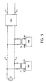
- the transmission system shown in Fig. 1 includes a plurality of transmitter circuits TR1/8 which are coupled in parallel to a transmission line L1, L2. More particularly, each of these transmitter circuits TR1 to TR8 has an output, with terminals L11, L21 to L18, L28, which is coupled to the line L1, L2 through a respective transformer T1/8. At its one end the transmission line L1, L2 is connected to a receiver circuit REC which is coupled to a digital exchange (not shown) through a subscriber line L3, L4, whilst at its other end it is terminated by an impedance Z1.
- Each of the transmitter circuits TR1/8 as well as the receiver circuit REC forms part of an S-interface circuit (not shown) which is able to perform the functions described above, e.g. to generate a current I, or -I, or no current between its output terminals L11 and L21/L18 and L28.
- the transmitter circuits TR1 to TR8 are indentical and therefore only one of them, i.e. TR1, and an associated control circuit CC which together with TR1 forms part of an S-interface is represented in detail in Fig. 2.
- the control circuit CC provides control signals X, XB, Y and YB which directly control the gates of the transistors P3 to P8 and N3 to N6.
- XB and YB are the inverse of X and Y respectively.
- the current source CS2 is in fact derived by current mirroring (not shown) from the accurate current source CS1. In this way a DC resistance which is not very accurate but sufficiently accurate is realised in a simple way.
- Their junction point A is connected to the non-inverting input of operational amplifier OA1 whose inverting input is connected to the junction point B of two parallel circuits which are both connected in series with resistor R2 between VDD and VSS.
- the first of these parallel circuits comprises the series connection of the source-to-drain paths of transistors P1 and P9 and the drain-to-source path of transistor N2.
- the second of these parallel circuits comprises the series connection of the source-to-drain paths of transistors P2 and P9 and the drain-to-source path of transistor N1.
- the gate of transistor P9 is controlled by the output signal of the operational amplifier OA2 whose inverting input is connected to the reference voltage VR and the non-inverting input of which is connected to the junction point C of transistors P7 and P8 which together with the transistor P1/6 and N1/N6 constitute a switching circuit.
- the drain-to-source paths of the transistors P7 and P8 are connected between terminal C and L11 and between terminal L21 and C respectively and their gates are controlled by the control signals X and Y respectively.
- the gates of transistors P1, P2, N1, N2 are controlled by the transistors P3 to P6 and N3 to N6 and permit the flow of current from the end L11 to the end L21 of P9 or vice-versa. More particularly, the source-to-drain paths of transistors P3 and P4 as well as the source-to-drain paths of transistors P5 and P6 are connected in series with the constant current source CS2 between VDD and VSS, and the junction points of P3 and P4 and of P5 and P6 are connected to the gates of P1 and P2 respectively.
- the gates of P3, P4, P5 and P6 are controlled by the respective control signals YB, XB, XB and YB provided by the control circuit CC.
- the gates of transistors N1 and N2 are controlled by the transistors N3, N4 and N5, N6 respectively.
- the drain-to-source paths of transistors N3 and N4 as well as the drain-to-source paths of transistors N5 and N6 are connected in series between the output of operational amplifier OA1 and VSS, and the junction points of N3 and N4 and of N5 and N6 are connected to the gates of N1 and N2 respectively.
- the gates of N3, N4, N5 and N6 are controlled by the respective control signals Y, X, X and Y provided by the control circuit CC.
- the operational amplifier OA2 together with the transistors P7, P8 and P9 constitutes a servo control circuit of which the forward path includes transistor P9 and the feedback path includes transistor P7 or P8.
- the operational amplifier OA1 has an input A to which the fixed voltage VA is applied and a feedback path which is closed via N3, N1 or via N5, N2.
- This operational amplifier OA1 together with R2 constitutes a constant current source by which the constant current I1 provided by CS1 is converted to a constant current I in R2.
- This current I flows from VDD to VSS via transistor P1, terminal L11, primary winding of transformer T1, terminal L21, transistor N2 and resistance R2.
- the constant current I1 is converted in the current I by multiplication with the ratio R1/R2. Because the current I1 may thus be chosen relatively small, the power consumption of the whole transmitter circuit is limited. On the other hand it is easier to realise an accurate ratio of resistances than to make accurate resistances.
- n 2.
- the output of the amplifier OA2 is therefore positive due to which transistor P9 is blocked.
- the voltage V across the terminals L11, L21 is limited to a constant value as soon as the current supplied to the receiver circuit REC is at least equal to 2I′.
- switching circuit P1/6, N1/6 in fact consists of four similar electronic contact devices P1/3/4, P2/5/6, N1/4/3 and N2/6/5.
- P1/3/4 includes :
Landscapes
- Engineering & Computer Science (AREA)
- Power Engineering (AREA)
- Computer Networks & Wireless Communication (AREA)
- Signal Processing (AREA)
- Amplifiers (AREA)
- Arrangements For Transmission Of Measured Signals (AREA)
- Superconductors And Manufacturing Methods Therefor (AREA)
- Cable Transmission Systems, Equalization Of Radio And Reduction Of Echo (AREA)
- Networks Using Active Elements (AREA)
- Alarm Systems (AREA)
- Selective Calling Equipment (AREA)
- Emergency Alarm Devices (AREA)
Claims (12)
- Circuit émetteur (TR1) pour un système de transmission dans lequel une pluralité de tels circuits émetteurs (TR1/8) sont couplés en parallèle à une ligne de transmission (L1, L2) qui est couplée à un circuit récepteur (REC), ledit circuit émetteur (TR1) ayant une sortie (L11, L21) qui est électriquement couplée à ladite ligne, mais est galvaniquement isolée de celle-ci et est capable de fournir à ladite sortie un courant (I) et de limiter ce courant en fonction de la tension sur ladite sortie, caractérisé sur ce que la sortie dudit circuit émetteur (L11, L12) est shunté par une impédance variable (P9) qui est commandée par la sortie d'un circuit d'asservissement (0A2, P7/8) qui répond en fonction de la différence entre une tension de référence (VR) et une tension de contre-réaction (VC) qui est elle-même fonction de la tension de sortie du circuit émetteur (V).
- Circuit émetteur conforme à la revendication 1, caractérisé en ce que ledit circuit d'asservissement (OA2, P7/8) comprend un circuit comparateur qui est constitué par un premier amplificateur opérationnel (OA2) dont les première et seconde entrées sont respectivement commandées par ladite tension de référence (VR) et ladite tension de contre-réaction (VC).
- Circuit émetteur conforme à la revendication 2, caractérisé en ce que ladite impédance variable (P9) est couplée, en série avec une source de courant (OA1, CS1, R1, R2), entre deux tensions d'alimentation continue (VDD, VSS) et en ce que l'extrémité de ladite impédance (P9) qui est connectée à ladite source de courant (OA1, CS1, R1, R2) est couplée à ladite seconde entrée dudit premier amplificateur opérationnel.
- Circuit émetteur conforme à la revendication 3, caractérisé en ce que ladite source de courant (OA1, CS1, R1, R2) comprend un deuxième amplificateur opérationnel (OA1) ayant une sortie qui est couplée, d'une part, à ladite second entrée et, d'autre part, à une première résistance (R2) qui est elle-même couplée en série avec ladite impédance variable (P9).
- Circuit émetteur conforme à la revendication 4, caractérisé en ce que la première entrée dudit deuxième amplificateur opérationnel (OA1) est connectée au point de jonction (A) d'une première source à courant constant (CS1) et d'une deuxième résistance (R1) qui font partie de ladite première source de courant mentionnée et sont couplées en série entre lesdites tensions continues (VDD, VSS), grâce à quoi une tension prédéterminée est fournie audit point de jonction (A).
- Circuit émetteur conforme à la revendication 2, caractérisé en ce que ladite impédance variable (P9) est un transistor de type PMOS dont la grille est commandée par la sortie dudit premier amplificateur opérationnel (OA2) et dont l'extrémité qui est connectée à ladite source de courant (OA1, CS1, R1, R2) est couplée à l'entrée non-inverseuse dudit premier amplificateur opérationnel (OA2).
- Circuit émetteur conforme à la revendication 1, caractérisé en ce qu'il est pourvu d'un système de contact électronique qui comprend au moins un dispositif de contact électronique incluant : un commutateur à transistor principal (P1; N2; P2; N1) connecté entre une dite première (VDD, VSS) et une deuxième (L11; L21; L21; L11) borne et ayant une troisième borne de commande; des premier (P3; N6; P5; N4) et deuxième (P4; N5; P6; N3) commutateurs auxiliaires à transistor respectivement connectés entre ladite troisième et une quatrième borne et entre ladite troisième borne et une cinquième borne; ainsi que des moyens de commande (CC) pour porter lesdits premiers (P3; N6; P5; N4) et deuxième (P4; N5; P6; N3) commutateurs auxiliaires à transistor dans des conditions opposées dans lesquelles l'un est bloqué et l'autre conducteur.
- Circuit émetteur conforme aux revendications 3 et 7, caractérisé en ce que lesdites première et quatrième bornes d'une part, et ladite deuxième borne, d'autre part, sont couplées chacune à une différente des deux dites tensions d'alimentation continues (VDD, VSS; VSS, VDD) et en ce que ladite cinquième borne est couplée à une troisième tension continue située entre lesdites deux tensions continues.
- Circuit émetteur conforme à la revendication 8, caractérisé en ce qu'il comprend au moins une paire desdits dispositifs qui est constituée par un premier (P1/3/4; P2/5/6) et un deuxième (N2/6/5; N1/4/3) desdits dispositifs de contact dont des premières bornes sont couplées à une première (VDD) et une deuxième (VSS) desdites tensions d'alimentation continues et dont des deuxièmes bornes sont couplées à des bornes différentes (L11, L21; L21, L11) de ladite impédance variable (P9).
- Circuit émetteur conforme aux revendications 3 et 9, caractérisé en ce que lesdites quatrième et cinquième bornes du premier dispositif (P1/3/4; P2/5/6) sont directement couplées respectivement à la première borne dudit dispositif et via une troisième résistance (CS2) à la quatrième borne du deuxième dispositif (N2/6/5; N1/4/3) et en ce que les quatrième et cinquième bornes du deuxième dispositif (N2/6/5; N1/4/3) sont respectivement couplées via ladite première résistance (R2) à la première borne dudit dispositif et, directement, à la sortie dudit deuxième amplificateur opérationnel (OA1) dont la première entrée et la sortie sont respectivement couplées aux première et cinquième bornes dudit deuxième dispositif (N2/6/5; N1/4/3), une tension prédéterminée (CS1, R1) étant appliquée à la deuxième entrée dudit deuxième amplificateur.
- Circuit émetteur conforme aux revendications 5 et 10, caractérisé en ce que ladite troisième résistance est fournie par une source à courant constant (CS2) qui est couplée à ladite première source à courant constant (CS1) connectée en série avec ladite deuxième résistance (R1) entre la première borne du premier dispositif et la quatrième borne du deuxième dispositif, ladite tension prédéterminée étant fournie eu point de jonction (A) de ladite première source à courant constant (CS1) et de ladite deuxième résistance (R1), ledit premier amplificateur opérationnel (OA2), lesdites première (R2) et deuxième (R1) résistances et ladite première source à courant constant (CS1) constituant ensemble ladite souce de courant.
- Circuit émetteur coforme à la revendication 11, caractérisé en ce qu'il comprend des première (P1/3/4; P2/5/6) et deuxième (N2/5/6; N1/3/4) paires desdits dispositifs, les premier et deuxième dispositifs de la première paire étant couplés aux première et deuxième bornes de ladite impédance variable, tandis que les premier et deuxième dispositifs de la deuxième paire sont couplés aux deuxième et première bornes de ladite impédance variable, et en ce que les première, quatrième et cinquième bornes des premiers dispositifs desdites paires, de même que des deuxièmes dispositifs de celles-ci, sont communes.
Priority Applications (1)
| Application Number | Priority Date | Filing Date | Title |
|---|---|---|---|
| AT88202851T ATE103747T1 (de) | 1987-12-23 | 1988-12-13 | Sendeschaltung. |
Applications Claiming Priority (2)
| Application Number | Priority Date | Filing Date | Title |
|---|---|---|---|
| BE8701480A BE1001413A6 (nl) | 1987-12-23 | 1987-12-23 | Zendketen en daarin gebruikt electronisch contactsysteem. |
| BE8701480 | 1987-12-23 |
Publications (3)
| Publication Number | Publication Date |
|---|---|
| EP0322025A2 EP0322025A2 (fr) | 1989-06-28 |
| EP0322025A3 EP0322025A3 (en) | 1990-04-25 |
| EP0322025B1 true EP0322025B1 (fr) | 1994-03-30 |
Family
ID=3883027
Family Applications (1)
| Application Number | Title | Priority Date | Filing Date |
|---|---|---|---|
| EP88202851A Expired - Lifetime EP0322025B1 (fr) | 1987-12-23 | 1988-12-13 | Circuit d'émission |
Country Status (6)
| Country | Link |
|---|---|
| EP (1) | EP0322025B1 (fr) |
| AT (1) | ATE103747T1 (fr) |
| AU (1) | AU613434B2 (fr) |
| BE (1) | BE1001413A6 (fr) |
| DE (1) | DE3888810T2 (fr) |
| ES (1) | ES2053716T3 (fr) |
Families Citing this family (2)
| Publication number | Priority date | Publication date | Assignee | Title |
|---|---|---|---|---|
| US4829541A (en) * | 1988-01-22 | 1989-05-09 | Advanced Micro Devices, Inc. | Pseudo-ternary code transmitter |
| US9210011B2 (en) * | 2011-09-23 | 2015-12-08 | Intel Corporation | Push-pull source-series terminated transmitter apparatus and method |
Family Cites Families (3)
| Publication number | Priority date | Publication date | Assignee | Title |
|---|---|---|---|---|
| GB1200486A (en) * | 1967-04-18 | 1970-07-29 | Int Computers Ltd | Data transmitting apparatus |
| DE2022553A1 (de) * | 1970-05-08 | 1971-11-25 | Siemens Ag | Anordnung zum Schutz vor Stoereinwirkungen in Anlagen der Nachrichten- bzw. Datentechnik |
| US4620310A (en) * | 1985-03-11 | 1986-10-28 | Metapath Inc. | Method and apparatus for generating bipolar pulses in a local area network |
-
1987
- 1987-12-23 BE BE8701480A patent/BE1001413A6/nl not_active IP Right Cessation
-
1988
- 1988-12-05 AU AU26527/88A patent/AU613434B2/en not_active Ceased
- 1988-12-13 ES ES88202851T patent/ES2053716T3/es not_active Expired - Lifetime
- 1988-12-13 EP EP88202851A patent/EP0322025B1/fr not_active Expired - Lifetime
- 1988-12-13 AT AT88202851T patent/ATE103747T1/de not_active IP Right Cessation
- 1988-12-13 DE DE3888810T patent/DE3888810T2/de not_active Expired - Fee Related
Also Published As
| Publication number | Publication date |
|---|---|
| DE3888810D1 (de) | 1994-05-05 |
| EP0322025A2 (fr) | 1989-06-28 |
| AU2652788A (en) | 1989-06-29 |
| EP0322025A3 (en) | 1990-04-25 |
| DE3888810T2 (de) | 1994-08-18 |
| ATE103747T1 (de) | 1994-04-15 |
| AU613434B2 (en) | 1991-08-01 |
| ES2053716T3 (es) | 1994-08-01 |
| BE1001413A6 (nl) | 1989-10-24 |
Similar Documents
| Publication | Publication Date | Title |
|---|---|---|
| US6130548A (en) | Signal converting receiver having constant hysteresis, and method therefor | |
| US5396028A (en) | Method and apparatus for transmission line termination | |
| US4581545A (en) | Schmitt trigger circuit | |
| DE2633066B1 (de) | Einrichtung zur uebertragung von gegentaktsignalen ueber eine zweidrahtleitung im duplexbetrieb | |
| US4797904A (en) | Transmitter for ISDN S-bus interface circuit | |
| WO1980001008A1 (fr) | Circuit d'accouplement pour transferer des signaux de donnee a une vitesse elevee | |
| US2662122A (en) | Two-way transistor electrical transmission system | |
| US4306119A (en) | Telephone outpulsing circuit | |
| US5614843A (en) | CMOS-PECL level conversion circuit | |
| EP0322025B1 (fr) | Circuit d'émission | |
| JPS63155931A (ja) | デジタル信号伝送回路 | |
| JP2000315923A (ja) | バースト光受信回路 | |
| US3476879A (en) | Line relay for d.c. telegraph systems | |
| GB1134371A (en) | Circuit arrangement for simultaneous signalling in both transmission directions between two terminal stations in telecommunication systems | |
| KR100408746B1 (ko) | 직류전압및교류전압디커플링용회로장치 | |
| US4899114A (en) | Voltage source amplifier for use in a pseudoternary code transmitter | |
| US3849607A (en) | Polarity reversal switching circuit | |
| US3689710A (en) | Two-wire to four-wire conversion circuit for a data switching center | |
| CN217587897U (zh) | 一种极性转换装置和无极性通讯系统 | |
| WO2000069071A1 (fr) | Pilote de mode de courant complementaire | |
| JP3130915B2 (ja) | データ伝送装置 | |
| IE811646L (en) | Circuit arrangement | |
| US2324394A (en) | Signaling system | |
| US2829205A (en) | Duplex signaling circuit | |
| JP2504455B2 (ja) | 極性反転検出回路 |
Legal Events
| Date | Code | Title | Description |
|---|---|---|---|
| PUAI | Public reference made under article 153(3) epc to a published international application that has entered the european phase |
Free format text: ORIGINAL CODE: 0009012 |
|
| AK | Designated contracting states |
Kind code of ref document: A2 Designated state(s): AT BE CH DE ES FR GB IT LI NL SE |
|
| PUAL | Search report despatched |
Free format text: ORIGINAL CODE: 0009013 |
|
| AK | Designated contracting states |
Kind code of ref document: A3 Designated state(s): AT BE CH DE ES FR GB IT LI NL SE |
|
| RHK1 | Main classification (correction) |
Ipc: H04L 25/08 |
|
| 17P | Request for examination filed |
Effective date: 19901019 |
|
| 17Q | First examination report despatched |
Effective date: 19920907 |
|
| GRAA | (expected) grant |
Free format text: ORIGINAL CODE: 0009210 |
|
| AK | Designated contracting states |
Kind code of ref document: B1 Designated state(s): AT BE CH DE ES FR GB IT LI NL SE |
|
| REF | Corresponds to: |
Ref document number: 103747 Country of ref document: AT Date of ref document: 19940415 Kind code of ref document: T |
|
| REF | Corresponds to: |
Ref document number: 3888810 Country of ref document: DE Date of ref document: 19940505 |
|
| ITF | It: translation for a ep patent filed | ||
| ET | Fr: translation filed | ||
| REG | Reference to a national code |
Ref country code: ES Ref legal event code: FG2A Ref document number: 2053716 Country of ref document: ES Kind code of ref document: T3 |
|
| EAL | Se: european patent in force in sweden |
Ref document number: 88202851.7 |
|
| PLBE | No opposition filed within time limit |
Free format text: ORIGINAL CODE: 0009261 |
|
| STAA | Information on the status of an ep patent application or granted ep patent |
Free format text: STATUS: NO OPPOSITION FILED WITHIN TIME LIMIT |
|
| 26N | No opposition filed | ||
| PGFP | Annual fee paid to national office [announced via postgrant information from national office to epo] |
Ref country code: GB Payment date: 19981112 Year of fee payment: 11 |
|
| PGFP | Annual fee paid to national office [announced via postgrant information from national office to epo] |
Ref country code: FR Payment date: 19981113 Year of fee payment: 11 |
|
| PGFP | Annual fee paid to national office [announced via postgrant information from national office to epo] |
Ref country code: SE Payment date: 19981118 Year of fee payment: 11 Ref country code: DE Payment date: 19981118 Year of fee payment: 11 |
|
| PGFP | Annual fee paid to national office [announced via postgrant information from national office to epo] |
Ref country code: NL Payment date: 19981123 Year of fee payment: 11 Ref country code: AT Payment date: 19981123 Year of fee payment: 11 |
|
| PGFP | Annual fee paid to national office [announced via postgrant information from national office to epo] |
Ref country code: CH Payment date: 19981124 Year of fee payment: 11 |
|
| PGFP | Annual fee paid to national office [announced via postgrant information from national office to epo] |
Ref country code: BE Payment date: 19981209 Year of fee payment: 11 |
|
| PGFP | Annual fee paid to national office [announced via postgrant information from national office to epo] |
Ref country code: ES Payment date: 19981216 Year of fee payment: 11 |
|
| PG25 | Lapsed in a contracting state [announced via postgrant information from national office to epo] |
Ref country code: GB Free format text: LAPSE BECAUSE OF NON-PAYMENT OF DUE FEES Effective date: 19991213 Ref country code: AT Free format text: LAPSE BECAUSE OF NON-PAYMENT OF DUE FEES Effective date: 19991213 |
|
| PG25 | Lapsed in a contracting state [announced via postgrant information from national office to epo] |
Ref country code: SE Free format text: LAPSE BECAUSE OF NON-PAYMENT OF DUE FEES Effective date: 19991214 |
|
| PG25 | Lapsed in a contracting state [announced via postgrant information from national office to epo] |
Ref country code: LI Free format text: LAPSE BECAUSE OF NON-PAYMENT OF DUE FEES Effective date: 19991231 Ref country code: CH Free format text: LAPSE BECAUSE OF NON-PAYMENT OF DUE FEES Effective date: 19991231 Ref country code: BE Free format text: LAPSE BECAUSE OF NON-PAYMENT OF DUE FEES Effective date: 19991231 |
|
| BERE | Be: lapsed |
Owner name: ALCATEL BELL Effective date: 19991231 |
|
| PG25 | Lapsed in a contracting state [announced via postgrant information from national office to epo] |
Ref country code: NL Free format text: LAPSE BECAUSE OF NON-PAYMENT OF DUE FEES Effective date: 20000701 |
|
| GBPC | Gb: european patent ceased through non-payment of renewal fee |
Effective date: 19991213 |
|
| EUG | Se: european patent has lapsed |
Ref document number: 88202851.7 |
|
| PG25 | Lapsed in a contracting state [announced via postgrant information from national office to epo] |
Ref country code: FR Free format text: LAPSE BECAUSE OF NON-PAYMENT OF DUE FEES Effective date: 20000831 |
|
| NLV4 | Nl: lapsed or anulled due to non-payment of the annual fee |
Effective date: 20000701 |
|
| PG25 | Lapsed in a contracting state [announced via postgrant information from national office to epo] |
Ref country code: DE Free format text: LAPSE BECAUSE OF NON-PAYMENT OF DUE FEES Effective date: 20001003 |
|
| REG | Reference to a national code |
Ref country code: FR Ref legal event code: ST |
|
| PG25 | Lapsed in a contracting state [announced via postgrant information from national office to epo] |
Ref country code: ES Free format text: LAPSE BECAUSE OF NON-PAYMENT OF DUE FEES Effective date: 20001214 |
|
| REG | Reference to a national code |
Ref country code: ES Ref legal event code: FD2A Effective date: 20010113 |
|
| PG25 | Lapsed in a contracting state [announced via postgrant information from national office to epo] |
Ref country code: IT Free format text: LAPSE BECAUSE OF NON-PAYMENT OF DUE FEES;WARNING: LAPSES OF ITALIAN PATENTS WITH EFFECTIVE DATE BEFORE 2007 MAY HAVE OCCURRED AT ANY TIME BEFORE 2007. THE CORRECT EFFECTIVE DATE MAY BE DIFFERENT FROM THE ONE RECORDED. Effective date: 20051213 |