EP0322030A2 - Dispositif pour la génération d'un courant en dent de scie - Google Patents
Dispositif pour la génération d'un courant en dent de scie Download PDFInfo
- Publication number
- EP0322030A2 EP0322030A2 EP19880202860 EP88202860A EP0322030A2 EP 0322030 A2 EP0322030 A2 EP 0322030A2 EP 19880202860 EP19880202860 EP 19880202860 EP 88202860 A EP88202860 A EP 88202860A EP 0322030 A2 EP0322030 A2 EP 0322030A2
- Authority
- EP
- European Patent Office
- Prior art keywords
- flyback
- pulse
- period
- transistor
- capacitor
- Prior art date
- Legal status (The legal status is an assumption and is not a legal conclusion. Google has not performed a legal analysis and makes no representation as to the accuracy of the status listed.)
- Withdrawn
Links
- 239000003990 capacitor Substances 0.000 claims abstract description 36
- 230000001939 inductive effect Effects 0.000 claims description 14
- 238000009877 rendering Methods 0.000 claims description 5
- 238000007599 discharging Methods 0.000 abstract 1
- 230000004048 modification Effects 0.000 description 4
- 238000012986 modification Methods 0.000 description 4
- 230000001965 increasing effect Effects 0.000 description 3
- 239000002800 charge carrier Substances 0.000 description 1
- 239000004020 conductor Substances 0.000 description 1
- 238000013016 damping Methods 0.000 description 1
- 238000010586 diagram Methods 0.000 description 1
- 230000000694 effects Effects 0.000 description 1
- 238000004519 manufacturing process Methods 0.000 description 1
- 238000000034 method Methods 0.000 description 1
- 230000000630 rising effect Effects 0.000 description 1
Images


Classifications
-
- H—ELECTRICITY
- H03—ELECTRONIC CIRCUITRY
- H03K—PULSE TECHNIQUE
- H03K4/00—Generating pulses having essentially a finite slope or stepped portions
- H03K4/06—Generating pulses having essentially a finite slope or stepped portions having triangular shape
- H03K4/08—Generating pulses having essentially a finite slope or stepped portions having triangular shape having sawtooth shape
-
- H—ELECTRICITY
- H03—ELECTRONIC CIRCUITRY
- H03K—PULSE TECHNIQUE
- H03K4/00—Generating pulses having essentially a finite slope or stepped portions
- H03K4/06—Generating pulses having essentially a finite slope or stepped portions having triangular shape
- H03K4/08—Generating pulses having essentially a finite slope or stepped portions having triangular shape having sawtooth shape
- H03K4/48—Generating pulses having essentially a finite slope or stepped portions having triangular shape having sawtooth shape using as active elements semiconductor devices
- H03K4/60—Generating pulses having essentially a finite slope or stepped portions having triangular shape having sawtooth shape using as active elements semiconductor devices in which a sawtooth current is produced through an inductor
- H03K4/62—Generating pulses having essentially a finite slope or stepped portions having triangular shape having sawtooth shape using as active elements semiconductor devices in which a sawtooth current is produced through an inductor using a semiconductor device operating as a switching device
Definitions
- the present invention relates to an arrangement for generating a sawtooth current having a stroke period and a flyback period through an inductive load, said arrangement comprising said inductive load, a storage capacitor, a unindirectional device through which said sawtooth current flows during a first part of each stroke period, a controlled switch through which said sawtooth current flows during the second part of each stroke period, a flyback capacitor connected in parallel with the main current path of said controlled switch, and a pulse source for supplying a pulse train for controlling the switching of said controlled switch.
- Such arrangements are well known and can take the form of a line deflection stage where the inductive load is formed by the scan or deflection coils and the storage capacitor is formed by the line trace capacitor.
- a stage of this type is normally arranged to operate at a single line frequency with a fixed flyback period being determined by the inductance and capacitance in circuit and principally the flyback capacitor.
- flyback time may be changed due to different input signal requirements.
- the line frequency may be changed from time to time in which case the flyback period would also need to be changed to achieve a given flyback period to scan period ratio.
- Such changes to the flyback period have in the past been achieved by changing the value of the flyback capacitor which can also require a switching arrangement to effect the change of capacitance which would give a single defined flyback time for each capacitance value.
- the invention provides an arrangement for generating a sawtooth current having a stroke period and a flyback period through an inductive load, said arrangement comprising said inductive load, a storage capacitor, a unidirectional device through which said sawtooth current flows during a first part of each stroke period, a controlled switch through which said sawtooth current flows during the second part of each stroke period, a flyback capacitor connected in parallel with the main current path of said controlled switch, and a pulse source for supplying a pulse train for controlling the switching of said controlled switch, characterised in that said arrangement additionally comprises switch means by which the flyback capacitor can be electrically isolated periodically from the inductive load and the storage capacitor when the voltage across the flyback capacitor has reached its peak value and for re-connecting the flyback capacitor thereto after a finite period for extending the flyback period.
- Such an arrangement has the advantage that only one flyback capacitor is required for various flyback periods and there is thus no need to provide a switching arrangement to switch between a number of flyback capacitors.
- a further advantage is that the peak voltage across the controlled switch is only proportional to the stroke period instead of being porportional to the stroke period divided by the flyback period as is the normal situation and as a result is considerably less effected by small order flyback period changes.
- the switch means comprises a bipolar transistor whose emitter-collector path is connected between said flyback capacitor and said inductive load, and a flyback time controller providing a pulse output for rendering said transistor non-conducting at or before the time at which said peak value is reached and conducting at said finite period after said time.
- the pulse train from the pulse source may then be applied to an input of said flyback time controller, the edge in the pulse train used to switch off said controlled switch being used to produce an edge in the pulse output from said flyback time controller to render said transistor non-conducting whilst an edge in said pulse output to render said transistor conducting is produced in response to a further input.
- Such an embodiment may require the pulse output of the flyback time controller to be amplified prior to it being applied to the transistor.
- the switch means comprises a thyristor whose main current path is connected between said flyback capacitor and said inductive load, and a flyback time controller providing a trigger pulse for rendering said thyristor conducting at the end of said finite period, said thyristor having become non-conducting during the stroke period when the polarity of the sawtooth current changes.
- the pulse train from said pulse source may then be applied as a gating pulse to an input of said flyback time controller, the controller producing the trigger pulse outside the period of said gating pulse.
- Such an embodiment has the advantage that the trigger pulse may be a short, predefined pulse instead of a signal with a specific duty cycle.
- Figure 1 shows a line deflection stage comprising a line oscillator LO which provides a pulse train at the appropriate line frequency.
- This pulse train is applied to a line driver circuit DR whose output provides drive pulses which are applied to the base of an n.p.n. bipolar line output transistor TR1 whose emitter is connected to earth.
- the collector of transistor TR1 is connected through a diode D1 and an inductor L to the positive supply voltage line +V A the negative line for which is connected to earth, this collector also being connected to the collector of a further n.p.n. bipolar transistor TR2.
- a flyback capacitor C f is connected between the emitter and collector electrodes of transistor TR1.
- the emitter of transistor TR2 is connected to a line deflection coil Ly which in turn is connected through a scan capacitor C s to earth whilst a diode D2 poled in the manner shown is connected in parallel with the deflection coil Ly and scan capacitor C s .
- a further diode D3 poled in the manner shown is connected between the emitter and collector electrodes of transistor TR2.
- the pulse train output of line oscillator LO is additionally applied to an input of a flyback time controller TC to a further input C of which a control voltage or signal is applied.
- the nature and operation of the flyback time controller TC will be described below in more detail.
- the pulse output of the controller TC is applied to the base of a further n.p.n. bipolar transistor TR3 whose collector is connected through the primary of a transformer T to the positive line of a low voltage supply +V B which primary is shunted by the series arrangement of a resistor R1 and a capacitor C1 for damping purposes.
- One end of the secondary of transformer T is connected to the emitter of transistor TR2 whilst the other end is connected through the parallel arrangement of a diode D4 poled in the manner shown and a resistor R2 to the base of transistor TR2.
- transistor TR2 conducts the whole time to provide a short circuit path across diode D3.
- the line output stage then operates in known manner with the voltage stored in scan capacitor C s producing the required sawtooth current through deflection coil Ly which initially flows through the diode D2 for a first part of a trace period and subsequently through transistor TR1 for a second part of the trace period.
- the flyback period is initiated at the instant transistor TR1 becomes non-conducting, which transistor has been previously rendered conducting prior to or at the commencement of the second part of the trace period, under the control of drive pulses from the driver circuit DR.
- the inductance and capacitance in the line output circuit resonate to produce a half sine wave flyback pulse which is followed by the start of a further scan period.
- Figure 2a shows pulses of the line frequency pulse train present at the output of the line oscillator LO and which may conveniently have a 1:1 mark-to-space ratio. These pulses are amplified by the driver stage DR and applied to the base of transistor TR1, the rising edges t1, t10 rendering the transistor conducting whilst the falling edges t2, t20 render the transistor non-conducting to initiate the flyback period.
- Figure 2c shows the flyback pulse present at the collector of transistor TR2 from which it will be seen that this transistor does not cease to conduct until time t3, t30 due to the charge carriers in the transistor.
- the line frequency pulse train is also applied to the flyback time controller TC which may be in the form of a flip-flop where the falling edges of this pulse train set the flip-flop into its '1' state whilst the time at which it is set into its '0' state is governed by the magnitude of a voltage applied to the control input C.
- Controller pulse outputs of various durations are shown in Figures 2b, 2d and 2f, these being applied to the base of transistor TR3 in which they are amplified and used to drive transistor TR2 by way of transformer T.
- Diode D4, resistor R2 and the leakage inductance of transformer T control the charge storage time of transistor TR2 and hence its turn-off characteristic as disclosed in our United Kingdom patent GB A 1 234 607.
- the drive to the base of transistor TR2 is arranged such that when the controller pulse output is in the '1' state the transistor is non-conducting and when in the '0' state the transistor conducts.
- transistor TR2 is only non-conducting for a short period between times t2 and t4, t20 and t40 and as the transistor conductors prior to the peak t5, t50 of the flyback pulse the flyback period is that as determined by the capacitance and inductive components of the deflection circuit and the flyback pulse is of normal half sine wave terminating at t6, t60 as shown in Figure 2c.
- the transistor TR2 is non-conducting for a longer period between times t2 and t6, t20 and t60 which includes the time t5, t50 at which the flyback pulse t5, t50 has reached its peak ( Figures 2e).
- the line deflection stage of Figure 1 may be used with different line frequencies and in particular with multi-line frequency data graphic displays where the flyback period can be increased as the line frequency is lowered to prevent the need to make the display substantially over-scan to enable the supplied video data to exploit the full useful display area on the picture tube. It can also be used with single frequency line deflection stages where the ratio between the scan and flyback period can be changed to accommodate different vision periods per line from different vision sources.
- the control voltage applied to the control input C of flyback time controller TC can be derived from a variable voltage source which can be manually adjusted or can be derived from the vision signal. In the latter case the control voltage may reflect the length of the blanking period.
- transistor TR2 is driven from the output of flyback time controller TC by way of a driver stage comprising transistor TR3, transformer T and associated components. If the single transitor TR2 were replaced by a multiple transistor of Darlington configuration then it could be possible to drive such a multiple transistor directly from the output of the time controller TC.
- Figure 3 shows a modification of the line deflection stage shown in Figure 1 and corresponding reference symbols used in the two figures indicate like components.
- the transistor TR2 is replaced by thyristor TH and because the level of drive required to cause the thyristor to conduct is substantially less than that required to render transistor TR2 conducting the drive circuitry associated with that transistor need not be required.
- the output of the flyback time controller TC is sufficient to drive thyristor TH.
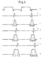
- the manner of operation of the deflection circuit of Figure 3 is substantially the same as that for Figure 1 with the duration of the flyback pulse being controlled by the time at which thyristor TH is rendered conducting. The detailed differences in operation will be described with additional reference to Figure 4 which shows waveforms associated with the line deflection stage of Figure 3.
- Figures 4a, 4c, 4e and 4g are the same as Figures 2a, 2c, 2e and 2g and show, as before, the output of the line oscillator LO and flyback pulses of an increasing duration.
- the transistor TR2 was periodically driven to provide a controlled period of non-conduction the thyristor TH of Figure 3 will automatically become non-conducting at or about the middle of the scan period when the polarity of the scan current reverses.
- the flyback period t3 t30 thyristor TH is already non-conducting.
- the flyback time controller TC is therefore required to produce a short trigger pulse at those times at which thyristor TH has to be rendered conducting in which state the thyristor TH remains until the next reversal of scan current. This is achieved by the magnitude or nature of the control voltage signal or signal applied to control input C, the input from the local oscillator LO acting as a gating pulse to prevent the flyback time controller TC from producing trigger pulses outside a given period following the start of the flyback period for which purpose the duration of the second part t1 to t2, t10 to t20 of the line oscillator LO output may be increased relative to its first part t2 to t10.
- the trigger pulse of Figure 4b can commence at or prior to the peak t5, t50 of the flyback pulse to ensure that the thyristor conducts at the occurrence of the peak. In the case shown the pulse occurs at t4, t40.
- the trigger pulse occurs at t6, t60 in Figure 4 whilst for Figure 4g the trigger pulse occurs at t7, t70.
Landscapes
- Details Of Television Scanning (AREA)
- Dc-Dc Converters (AREA)
Applications Claiming Priority (2)
| Application Number | Priority Date | Filing Date | Title |
|---|---|---|---|
| GB8729516 | 1987-12-18 | ||
| GB8729516A GB2214016A (en) | 1987-12-18 | 1987-12-18 | Variable flyback period |
Publications (2)
| Publication Number | Publication Date |
|---|---|
| EP0322030A2 true EP0322030A2 (fr) | 1989-06-28 |
| EP0322030A3 EP0322030A3 (fr) | 1991-03-27 |
Family
ID=10628678
Family Applications (1)
| Application Number | Title | Priority Date | Filing Date |
|---|---|---|---|
| EP19880202860 Withdrawn EP0322030A3 (fr) | 1987-12-18 | 1988-12-13 | Dispositif pour la génération d'un courant en dent de scie |
Country Status (5)
| Country | Link |
|---|---|
| US (1) | US4890043A (fr) |
| EP (1) | EP0322030A3 (fr) |
| JP (1) | JPH01195780A (fr) |
| KR (1) | KR890011210A (fr) |
| GB (1) | GB2214016A (fr) |
Families Citing this family (6)
| Publication number | Priority date | Publication date | Assignee | Title |
|---|---|---|---|---|
| US5115171A (en) * | 1991-01-04 | 1992-05-19 | Rca Licensing Corporation | Raster distortion correction circuit |
| GB9100123D0 (en) | 1991-01-04 | 1991-02-20 | Rca Licensing Corp | Raster corrected horizontal deflection |
| GB9215993D0 (en) * | 1992-07-28 | 1992-09-09 | Rca Thomson Licensing Corp | Raster corrected horizontal defelction |
| US5841248A (en) * | 1997-04-30 | 1998-11-24 | Rca Thomson Licensing Corporation | Charge controlled raster correction circuit |
| US6320332B1 (en) | 1999-10-08 | 2001-11-20 | Thomson Licensing S.A. | Raster distortion correction circuit |
| TWI459855B (zh) * | 2012-10-19 | 2014-11-01 | Raydium Semiconductor Corp | 具有維持電流電路之發光二極體驅動裝置及其運作方法 |
Family Cites Families (6)
| Publication number | Priority date | Publication date | Assignee | Title |
|---|---|---|---|---|
| US4400652A (en) * | 1982-05-03 | 1983-08-23 | Squibb Vitatek, Inc. | Magnetic deflection sweep amplifier with intelligent flyback |
| NL8202499A (nl) * | 1982-06-21 | 1984-01-16 | Philips Nv | Schakelinrichting voor een beeldweergeefinrichting voor het opwekken van een zaagtandvormige lijnafbuigstroom. |
| US4607195A (en) * | 1983-03-21 | 1986-08-19 | U.S. Philips Corporation | Picture display device comprising a power supply circuit and a line deflection circuit |
| US4590408A (en) * | 1984-05-08 | 1986-05-20 | Systems Research Laboratories, Inc. | Linear/resonant CRT beam deflection circuit |
| JPH0813094B2 (ja) * | 1985-04-19 | 1996-02-07 | 日本ビクター株式会社 | 水平偏向回路 |
| GB2177270A (en) * | 1985-06-19 | 1987-01-14 | Philips Electronic Associated | Line output circuit for generating a sawtooth current at two frequencies |
-
1987
- 1987-12-18 GB GB8729516A patent/GB2214016A/en not_active Withdrawn
-
1988
- 1988-11-02 US US07/266,182 patent/US4890043A/en not_active Expired - Fee Related
- 1988-12-13 EP EP19880202860 patent/EP0322030A3/fr not_active Withdrawn
- 1988-12-15 KR KR1019880016687A patent/KR890011210A/ko not_active Withdrawn
- 1988-12-19 JP JP63318694A patent/JPH01195780A/ja active Pending
Also Published As
| Publication number | Publication date |
|---|---|
| GB2214016A (en) | 1989-08-23 |
| JPH01195780A (ja) | 1989-08-07 |
| US4890043A (en) | 1989-12-26 |
| EP0322030A3 (fr) | 1991-03-27 |
| GB8729516D0 (en) | 1988-02-03 |
| KR890011210A (ko) | 1989-08-14 |
Similar Documents
| Publication | Publication Date | Title |
|---|---|---|
| US4837457A (en) | High voltage power transistor circuits | |
| US4471327A (en) | Self-oscillating power supply | |
| EP0322030A2 (fr) | Dispositif pour la génération d'un courant en dent de scie | |
| EP0185481B1 (fr) | Appareil commutateur à résonance utilisant un montage en cascode | |
| US4733141A (en) | Horizontal output circuit for correcting pin cushion distortion of a raster | |
| US4695774A (en) | Line output circuit for generating a line frequency sawtooth current | |
| KR900008233B1 (ko) | 수평 편향 귀선 시간 절환 회로 | |
| US5084811A (en) | Progressive start up device for a switching power supply | |
| CA1147454A (fr) | Circuit de deviation verticale commutee synchrone attaque durant les intervalles d'avance et de retour du spot | |
| US3323001A (en) | Time-base circuit arrangement having transistor and scr switching elements | |
| JPH0372783A (ja) | サイン波偏向回路 | |
| US4362974A (en) | Commutated switched regulator with line isolation for transistor deflection | |
| US4481431A (en) | Circuit for driving a switching transistor | |
| GB2045564A (en) | Commutated switched regulator with line isolation for transistor deflection | |
| JP2635553B2 (ja) | 入力周波数で出力電流を発生させる装置 | |
| US3809947A (en) | Sine wave deflection system for correcting pincushion distortion | |
| EP0272744A2 (fr) | Montage à transistor bipolaire haute-tension | |
| KR950001803Y1 (ko) | 모니터의 화면 리플잡음 제거회로 | |
| SU1637027A1 (ru) | Генератор телевизионной строчной развертки | |
| CA1283478C (fr) | Generateur de courant de deviation verticale | |
| US3435280A (en) | Deflection circuit | |
| KR100203404B1 (ko) | 편향구동회로 | |
| US4415842A (en) | Television receiver start-up circuit | |
| GB2198899A (en) | Circuit arrangement with two serially connected high-voltage switches | |
| GB2198896A (en) | Circuit arrangement with a high voltage switch |
Legal Events
| Date | Code | Title | Description |
|---|---|---|---|
| PUAI | Public reference made under article 153(3) epc to a published international application that has entered the european phase |
Free format text: ORIGINAL CODE: 0009012 |
|
| AK | Designated contracting states |
Kind code of ref document: A2 Designated state(s): DE FR GB IT SE |
|
| PUAL | Search report despatched |
Free format text: ORIGINAL CODE: 0009013 |
|
| AK | Designated contracting states |
Kind code of ref document: A3 Designated state(s): DE FR GB IT SE |
|
| 17P | Request for examination filed |
Effective date: 19910923 |
|
| RAP3 | Party data changed (applicant data changed or rights of an application transferred) |
Owner name: N.V. PHILIPS' GLOEILAMPENFABRIEKEN Owner name: PHILIPS ELECTRONICS UK LIMITED |
|
| 17Q | First examination report despatched |
Effective date: 19930705 |
|
| STAA | Information on the status of an ep patent application or granted ep patent |
Free format text: STATUS: THE APPLICATION IS DEEMED TO BE WITHDRAWN |
|
| 18D | Application deemed to be withdrawn |
Effective date: 19940311 |