EP0322769B1 - Dispositif de traitement de données adapté à un traitement de grande vitesse - Google Patents
Dispositif de traitement de données adapté à un traitement de grande vitesse Download PDFInfo
- Publication number
- EP0322769B1 EP0322769B1 EP88121516A EP88121516A EP0322769B1 EP 0322769 B1 EP0322769 B1 EP 0322769B1 EP 88121516 A EP88121516 A EP 88121516A EP 88121516 A EP88121516 A EP 88121516A EP 0322769 B1 EP0322769 B1 EP 0322769B1
- Authority
- EP
- European Patent Office
- Prior art keywords
- micro
- instruction
- address
- branch
- subsequent
- Prior art date
- Legal status (The legal status is an assumption and is not a legal conclusion. Google has not performed a legal analysis and makes no representation as to the accuracy of the status listed.)
- Expired - Lifetime
Links
Images


Classifications
-
- G—PHYSICS
- G06—COMPUTING OR CALCULATING; COUNTING
- G06F—ELECTRIC DIGITAL DATA PROCESSING
- G06F9/00—Arrangements for program control, e.g. control units
- G06F9/06—Arrangements for program control, e.g. control units using stored programs, i.e. using an internal store of processing equipment to receive or retain programs
- G06F9/22—Microcontrol or microprogram arrangements
- G06F9/26—Address formation of the next micro-instruction ; Microprogram storage or retrieval arrangements
-
- G—PHYSICS
- G06—COMPUTING OR CALCULATING; COUNTING
- G06F—ELECTRIC DIGITAL DATA PROCESSING
- G06F9/00—Arrangements for program control, e.g. control units
- G06F9/06—Arrangements for program control, e.g. control units using stored programs, i.e. using an internal store of processing equipment to receive or retain programs
- G06F9/22—Microcontrol or microprogram arrangements
- G06F9/26—Address formation of the next micro-instruction ; Microprogram storage or retrieval arrangements
- G06F9/262—Arrangements for next microinstruction selection
- G06F9/264—Microinstruction selection based on results of processing
Definitions
- the present invention relates to a micro-program control type data processing apparatus and, more particularly, to a microprocessor suitable for high speed processing.
- the micro-program control type data processing apparatus of the prior art produces control signals in response to a micro-instruction fetched from a micro-program storing memory, as is disclosed on pp. 97 to 107 of Micro-Electronics 8 of Iwanami Series "VLSI Computer” edited by Tatsushi Motooka.
- Fig. 2 shows an example of the structure of the microprocessor investigated by us on the basis of the prior art before the present application has been filed.
- a pipe line processing stage is divided into four: an instruction fetch by an instruction fetch unit 101; a first instruction decoding (i.e., instruction decoder) by an instruction decoder 111 of an instruction decoding unit 102; a second instruction decoding (i.e., micro ROM) by a micro ROM 113 of the instruction decoding unit 102; and an instruction execution by an instruction execution unit 103. Since these four states are processed in parallel, the present microprocessor executes the so-called "pipeline processing".
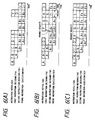
- Fig. 6 shows the flow chart of the pipeline processing in the normal operation of the present microprocessor.
- the abscissa indicates the time, and the ordinate indicates each processing stage.
- the parenthesized numerals indicating the individual stages in Fig. 6(A) designate the signals at the inputs of the circuit, as designated at corresponding numerals in Fig. 2.
- Reference letters A to F in Fig. 6(A) designate individual macro-instructions.
- Each macro-instruction is fetched by the instruction fetch unit 101 from either the main memory outside of the microprocessor or the cache memory in the microprocessor and is decoded by the instruction decoder 111 to provide a micro-address 121. If the instruction A is decoded by the instruction decoder 111, for example, a micro-address MA1 is produced.
- This micro-address indicates the top address of a sub-routine A1 of the micro-program stored in the micro ROM 113.
- micro-addresses MA1, MA2, MA3 and MA4 correspond to a series of micro-program sub-routines A1, A2 and A3 constituting one micro-instruction A.
- the micro ROM 113 is searched so that the execution unit 103 is controlled on the basis of a micro-instruction 136.
- the instruction execution is successively accomplished in the normal pipeline processing so that the micro-processor can process the instruction at a high speed.
- Another example of the prior art is given in the document EP-A- 0 190 484.
- Fig. 6(B) shows the flow chart of the processing in which the microprocessor executes a branch instruction to accomplish a branch processing.
- a vacant time is established in the instruction execution to drop the execution speed of the instruction. This is because a branch has occurred upon the execution of the instruction A.
- the microprocessor pre-fetches the instruction, assuming that the instructions be executed sequentially in the order of A, B, C, D, ..., and so on. If a branch takes place, however the instruction F is executed after the instruction A as in this example so that the pre-fetch of the instruction is useless. This processing disturbance appears as the vacant time of the execution unit.
- the branch macro-instruction A is a conditional branch instruction
- the conditional branch instruction A is executed at the four steps: the micro-instruction A1, i.e., the step for executing a condition discrimination; the micro-instruction A2 for actually executing the branch in accordance with the result of the condition discrimination; the micro-instruction A3 for decoding a subsequent instruction in either case of the branch formation or non-formation; and the micro-instruction A4 for declaring the end of the branch macro-instruction A, and the pipeline processing is constructed of the four step: the instruction fetch, the first instruction decoding, the second instruction decoding and the instruction execution, as described above.
- the signal processing of the circuit such as the instruction fetch unit, the instruction decoding unit or the instruction execution unit of a single chip microprocessor having a semiconductor device (e.g., a MOSFET of 1.3 micronrule), which is formed on a semiconductor chip by using the fine semiconductor process, goes on increasing the speed.
- a semiconductor device e.g., a MOSFET of 1.3 micronrule
- Claim 1 It is, therefore, an object of the present invention as defined in Claim 1 to provide a pipeline data processing apparatus in which the time interval between the executions of a conditional branch instruction and a subsequent instruction is shortened.
- a data processing apparatus comprising:
- the first micro-instruction (A1) which is outputted from the micro-program storing memory (113) of the instruction decoding unit (102), contains only the information relating to the conditional discrimination for the conditional branch but not any information requesting the branch ready.
- the microprogram storing memory (113) outputs both the information relating to the conditional discrimination for the conditional branch as the first micro-instruction (A1) and the second micro-address (MA2) as the subsequent micro-address in response to the first micro-address (MA1).
- the micro-address generating circuit (115) generates the second micro-address (MA2) as the subsequent micro-address.
- the micro-program storing memory (113) outputs the information (126) requesting the branch as the second micro-instruction (A2). At this time, the actual branch is executed by the conditional branch instruction.
- the scale of the micro-program storing memory (113) is accordingly enlarged.
- the instant, at which the micro-program storing memory (113) outputs the information (126) requesting the branch as the second micro-instruction (A2) in response to the second micro-address (MA2) is necessarily delayed.
- the fetch time of the branch target instruction is also delayed to establish an innegligible vacant time between the execution of the conditional branch instruction and the execution of the subsequent instruction as the branch target instruction.
- the first micro-instruction (A1) which is outputted from the micro-program storing memory (113) of said instruction decoding unit (102) in response to the first micro-address (MA1), contains both the information relating to the conditional discrimination for the conditional branch and the information (126′) requesting the branch ready.
- the signal analyzing circuit (130) which generates the branch request signal (131) to be fed to the branch control circuit (114) of the instruction fetch unit (101), in response to both the branch ready request information (126′) and the second micro-address (MA2) which is generated as the subsequent micro-address from the micro-address generating circuit (115) when the branch condition of the conditional branch instruction is formed.
- the micro-program storing memory (113) in response to the first micro-address (MA1), the micro-program storing memory (113) outputs the information relating the conditional discrimination for the conditional branch as the first micro-instruction (A1) and the second micro-address (MA2) as the subsequent micro-address.
- the micro-address generating circuit (115) generates the second micro-address (MA2) as the subsequent micro-address.
- the actual branch according to the conditional branch instruction is requested by the branch request signal (131) of the signal analyzing circuit (130) so that the subsequent instruction as the branch target instruction can be early fetched. This makes it possible to shorten the vacant time between the execution of the conditional branch instruction and the execution of the subsequent instruction as the branch target instruction.
- Fig. 1 shows an example of the structure of the microprocessor according to the present invention.
- a microprocessor 100 is composed mainly of an instruction fetch unit 101, an instruction decoding unit 102 and an instruction execution unit 103.
- the instruction fetch unit 101 fetches a macro-instruction from a main memory outside of the microprocessor or a cache memory inside of the microprocessor.
- the macro-instruction thus fetched is sent to the instruction decoding unit 102, in which it is decoded at two stages of an instruction decoder 111 and a micro-ROM 113.
- the instruction execution unit 103 executes the instruction.
- the instruction decoder 111 decodes the macro-instruction coming from the instruction fetch unit 101 and outputs the decoded result of 60 bits containing a micro-address to a latch circuit 116.
- the micro-address i.e., the decoded result outputted from the latch circuit 116 is inputted through a selector 117 and an address decoder 112 to the micro-ROM 113 so that a micro-instruction 118 of 135 bits is obtained as an ROM access.
- the micro-instruction 118 contains not only an information 136 for controlling the execution unit 103 but also a subsequent micro-address information 127 of 12 bits. This subsequent micro-address 127 is inputted again through a micro-address generating circuit 115 and the selector 117 to the micro-ROM 113 so that a subsequent micro-instruction is fetched.
- the instruction decoder 111 outputs the top micro-address of a sub-program composed of the micro-instruction.
- Fig. 6(A) for example, if an instruction A is decoded, the top micro-address A1 of the sub-program is outputted.
- the micro-program storing memory (i.e., micro-ROM) 113 In response to the top micro-address generated by the instruction decoder 111, the micro-program storing memory (i.e., micro-ROM) 113 generates both a micro-instruction for controlling the instruction execution unit 103, the micro-address generating circuit 115 and a branch control circuit 114 and a subsequent micro-address information relating to the micro-address of a subsequent micro-instruction to be executed after the micro-instruction. In response to the subsequent micro-address generated from the output of the micro-address generating circuit 115 and fed through the selector 117, moreover, the micro-ROM 113 outputs a succeeding subsequent micro-instruction and a succeeding subsequent micro-address information.
- micro-ROM 113 In response to the subsequent micro-address generated from the output of the micro-address generating circuit 115 and fed through the selector 117, moreover, the micro-
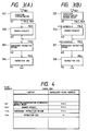
- Fig. 4 shows the content of the micro-ROM 113.
- the lefthand of Fig. 4 shows the micro-address to be fed to the micro-ROM 113; the center of Fig. 4 shows the content of the micro-instruction to be generated from the micro-ROM 113 in response to each micro-address; and the righthand of Fig. 4 shows the subsequent micro-address to be generated from the micro-ROM 113 in response to each micro-address.
- micro-addresses MA1, MA2, MA3 and MA4 constitute a conditional branch micro-instruction A. If the conditional branch macro-instruction A is fed to the instruction decoding unit 102 through the instruction fetch unit 101 from the main memory outside of the microprocessor or the cache memory inside of the microprocessor, the instruction decoder 111 generates the top micro-address MA1 for the conditional branch.
- the micro-ROM 113 In response to the top micro-address MA1, the micro-ROM 113 outputs not only both the information relating to the conditional discrimination for the conditional branch and the information 126′ requesting the branch ready as the first micro-instruction but also the second micro-address MA2 subsequent to the first micro-address MA1 as a subsequent micro-address.
- this branch ready request information indicated by a signal 126′ of 1 bit is fed from the output of the micro-ROM 113 through the latch circuit 118 to a later-described micro-address analyzing circuit 130.
- this micro-ROM 113 If this second micro-address MA2 is fed through the selector 117 to the input of the micro-ROM 113, this micro-ROM 113 outputs the information requesting the branch as the second micro-instruction A2 and the third micro-address MA3 subsequent to the second micro-address MA2 as a subsequent micro-address.
- the second micro-address MA2 is disposed at an even address
- the third micro-address MA3 is disposed at an odd address
- this micro-ROM 113 When this third micro-address MA3 is fed through the selector 117 to the input of the micro-ROM 113, this micro-ROM 113 outputs the information requesting a subsequent instruction decoding as the third micro-instruction M3 and the fourth micro-address MA4 subsequent to the third micro-address MA4 as a subsequent micro-address.
- this micro-ROM 113 If this fourth micro-address MA4 is fed through the selector 117 to the input of the micro-ROM 113, this micro-ROM 113 outputs the information declaring the end of the branch instruction as the fourth micro-instruction M4. At this declaration of the end of the branch instruction, however, any subsequent micro-address is outputted.
- the instruction decoder 111 If the conditional branch macro-instruction A is fed from the main memory outside of the micro-processor 100 or the cache memory inside of the same through the instruction fetch unit 101 to the instruction decoding unit 102, the instruction decoder 111 generates the top micro-address MA1 for the conditional branch. In response to this top micro-address MA1, the micro-ROM 113 outputs not only both the information relating to the conditional discrimination for the conditional branch and the information 126′ requesting the branch ready as the first micro-instruction A1 but also the second micro-address MA2 subsequent to the first micro-address MA1 as a subsequent micro-address.
- the micro-address generating circuit 115 discriminates the formation or non-formation of the condition for the conditional branch.
- the micro-address generating circuit 115 When the condition is formed, the micro-address generating circuit 115 generates the second micro-address MA2 as a subsequent micro-address.
- the micro-address generating circuit 115 When the condition is not formed, on the contrary, the micro-address generating circuit 115 generates the third micro-address MA3 as a subsequent micro-address.
- the signal analyzing circuit 130 for generating a branch requesting signal 131 to be fed to the branch control circuit 114 of the instruction fetch unit 101, in response to both the branch ready request information 126′ and the second micro-address MA2 at an even address, which is generated as a subsequent micro-address from the micro-address generating circuit 115 when the branch condition of the conditional branch instruction is formed.
- the even address is generated as a subsequent micro-address from the micro-address generating circuit 115.
- the odd address is generated as a subsequent micro-address from the micro-address generating circuit 115.
- the formation or non-formation of the branch condition of the conditional branch instruction can be discriminated by monitoring the LSB (i.e., Least Significant Bit) signal of 1 bit of the address signal generated from the micro-address generating circuit 115.
- this LSB signal is a signal 124 of 1 bit which is fed from the output of the micro-address generating circuit 115 through the selector 117 to the micro-address analyzing circuit 130. If this LSB signal 124 is at the "0" level, the branch condition of the conditional branch instruction is formed so that the even address is generated as the subsequent micro-address from the micro-address generating circuit 115. If the LSB signal 124 is at the "1" level, the branch condition of the conditional branch instruction is not formed so that the odd address is generated as the subsequent micro-address from the micro-address generating circuit 115.
- the micro-address analyzing circuit 130 outputs the branch request signal 131 in response to the LSB signal 124 at the "0" level and the branch ready request information 126′.
- the instruction decoder 111 responds to that unconditional branch macro-instruction and output an unconditional branch instruction discrimination signal 122.
- This unconditional branch instruction discrimination signal 122 is fed through the latch circuit 116 to the micro-address analyzing circuit 130.
- the micro-address analyzing circuit 130 outputs the branch request signal 131 in response to the instruction end micro-instruction 126 ⁇ and the unconditional branch instruction discrimination signal 122 so that the instruction fetch unit 101 starts an early fetch of a subsequent instruction of the branch target.
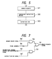
- Fig. 7 shows one example of the structure of the micro-address analyzing circuit 130.
- the branch condition of the conditional branch instruction is formed, the output 700 of one AND circuit is asserted.
- the unconditional branch instruction is fetched and decoded, the output 701 of the other AND circuit is asserted.
- the branch request signal 131 is generated from the output of the OR circuit.
- Fig. 3(A) shows the signal processing operations relating to the conditional branch instruction of the microprocessor investigated before the application of the present invention, as shown in Fig. 2.
- the instruction decoder 111 if the conditional branch macro-instruction A is fed to the instruction decoding unit 102 from the main memory outside of the microprocessor or the cachememory inside of the same, the instruction decoder 111 generates the top micro-address MA1 for the conditional branch.
- the micro-ROM 113 In response to this top micro-address MA1, at Step 301 of Fig. 3(A), the micro-ROM 113 outputs the information relating to the conditional discrimination for the conditional branch as the first micro-instruction and the second micro-address MA2 subsequent to that micro-address MA1 as the subsequent micro-address.
- the micro-address generating circuit 115 outputs the second micro-address MA2 as the subsequent micro-address if the branch condition of the conditional branch instruction is formed.
- the branch is not requested before the output stage of Step 302 of Fig. 3(A), at which the micro-ROM 113 outputs a branch request information 126 in response to that second micro-address MA2.
- a vacant time exists between the execution of the conditional branch instruction and the execution of the subsequent instruction, as shown in Fig. 6(B). If the branch condition of the conditional branch instruction is not formed, on the contrary, the micro-address generating circuit 115 outputs the third micro-address MA3 as the subsequent micro-address at that step 301.
- the micro-ROM In response to this third micro-address MA3, at Step 303 of Fig. 3(A), the micro-ROM outputs both the information requesting the subsequent instruction decoding as the third micro-instruction A3 and the fourth micro-address MA4. In response to this fourth micro-address MA4, at Step 304 of Fig. 3(A), the micro-ROM 113 outputs the information declaring the end of the branch instruction as the fourth micro-instruction A4.
- the signal processing operations of the microprocessor of the present embodiment shown in Fig. 1 can process the conditional branch instruction at a high speed, as will be described in the following.
- conditional branch macro-instruction A is fed to the instruction decoding unit 102 from the main memory outside of the microprocessor or inside cache of the same, as described hereinbefore, the instruction decoder 111 generates the top micro-address MA1 for the conditional branch.
- the micro-ROM 113 In response to the top micro-address MA1, at Step 301 of Fig. 3(B), the micro-ROM 113 outputs not only both the information relating to the conditional discrimination for the conditional branch and the information 126′ requesting the branch ready as the first micro-instruction but also the second micro-address MA2 of an even address subsequent to that micro-address MA1 as the subsequent micro-address.
- the micro-address generating circuit 115 outputs the second micro-address MA2 as the subsequent micro-address.
- the branch is requested already at the input stage of Step 306 of Fig. 3(B), at which the micro-address analyzing circuit 130 outputs the branch request information 126′ as the second micro-instruction A2 in response to the branch ready request information 126′ and the second micro-address MA2 at the even address.
- the micro-address generating circuit 115 outputs the third micro-address MA3 of the odd address as the subsequent micro-address.
- the micro-ROM 113 outputs both the information requesting the subsequent instruction decoding as the third micro-instruction A3 and the fourth micro-address MA4.
- the micro-ROM 113 outputs the information declaring the end of the branch instruction as the fourth micro-instruction A4.
- Fig. 5 shows a signal processing flow chart for processing the unconditional branch instruction.
- the information requesting the unconditional branch is outputted as the first micro-instruction, and the second micro-address subsequent to that top first micro-address is outputted as the subsequent micro-address.
- the information requesting the subsequent instruction decode is outputted as the second micro-instruction, and the third micro-address is outputted.
- the information declaring the end of the branch instruction is outputted as the third micro-instruction.
- the Step 501 of Fig. 5 is executed at the two stages of the first instruction decoding of the instruction decoder 111 of the instruction decoding unit 102 and the second instruction decoding of the micro-ROM 113.
- the unconditional branch decoding signal 122 obtained from the result of the first instruction decoding of the Step 501 is fed to the micro-address analyzing circuit 130 so that the high-speed branch request is accomplished in response to the branch request signal of the micro-address analyzing circuit 130.
- the branch request information as the second micro-instruction A2 of Fig. 4 needs not actively request the branch any more, it may have a content requesting the branch passively.
- the information content of the passive branch request can be constructed of the information content by which the branch ready of the first micro-instruction A1 is not cancelled.
- the information content of this passive branch request also corresponds to the information requesting the branch by the technical concept of the present invention.
- the content of the subsequent instruction to be fetched is different in dependence upon the formation or non-formation of the branch condition of the conditional branch instruction, but the branch request is made at an early stage in response to the subsequent micro-address information of a specific address, which is generated from the micro-address circuit when the branch condition is formed, so that the time interval between the execution of the conditional branch instruction and the execution of the subsequent instruction can be shortened.
Landscapes
- Engineering & Computer Science (AREA)
- Software Systems (AREA)
- Theoretical Computer Science (AREA)
- Physics & Mathematics (AREA)
- General Engineering & Computer Science (AREA)
- General Physics & Mathematics (AREA)
- Advance Control (AREA)
- Executing Machine-Instructions (AREA)
Claims (4)
- Dispositif de traitement de données, en particulier un microprocesseur, comprenant(1) une unité (101) de lecture d'instruction pour lire une instruction stockée dans un moyen formant mémoire;(2) une unité (102) de décodage d'instruction pour décoder l'instruction lue par ladite unité (101) de lecture d'instruction; et(3) une unité (103) d'exécution d'instruction conçue pour être commandée par le signal de sortie de ladite unité (102) de décodage d'instruction,dans lequel ladite unité (101) de lecture d'instruction comporte
(1a) un circuit (114) de commande de branchement pour lire une instruction cible de branchement, stockée dans ledit moyen formant mémoire, en réponse à un signal de demande de branchement issu de ladite unité de décodage d'instruction,
dans lequel ladite unité (102) de décodage d'instruction comporte:(2a) un décodeur (111) d'instruction pour produire une micro-adresse en réponse à l'instruction lue par ladite unité (101) de lecture d'instruction;(2b) une mémoire (113) de stockage de microprogramme réagissant à la micro-adresse produite par ledit décodeur (111) d'instruction pour produire à la fois une micro-instruction pour commander ladite unité (103) d'exécution d'instruction et une information suivante de micro-adresse concernant la micro-adresse d'une micro-instruction suivante à exécuter après ladite micro-instruction; et(2c) un circuit (115) générateur de micro-adresses pour générer une micro-adresse suivante en réponse au moins à ladite information suivante de micro-adresse produite par ladite mémoire (113) de stockage de micro-programme et à une information (128) concernant le résultat de l'exécution d'instruction produite par ladite unité (103) d'exécution d'instruction,dans lequel le décodeur (111) d'instruction de ladite unité (102) de décodage d'instruction génère une première micro-adresse (MA1) pour un branchement conditionnel en réponse à une instruction (A) de branchement conditionnel extraite de ladite unité de lecture d'instruction,
dans lequel la mémoire (113) de stockage de micro-programme de ladite unité (102) de décodage d'instruction réagit à ladite première micro-adresse (MA1) pour ledit branchement conditionnel de façon à produire à la fois une information concernant la discrimination conditionnelle pour ledit branchement conditionnel et une information (126˝) demandant un branchement prêt en tant que micro-instruction et à générer une seconde micro-adresse (MA2) à la suite de ladite première micro-adresse (MA1) en tant que micro-adresse suivante,
dans lequel la mémoire (113) de stockage de micro-programme de ladite unité (102) de décodage d'instruction réagit à la seconde micro-adresse (MA2) de façon à générer une troisième micro-adresse (MA3) à la suite de ladite seconde micro-adresse (MA2) en tant que micro-adresse suivante,
dans lequel la mémoire (113) de stockage de micro-programme de ladite unité (102) de décodage d'instruction réagit à ladite troisième micro-adresse (MA3) pour produire en tant que micro-instruction (M3) une information demandant un décodage d'instruction suivante,
dans lequel ledit circuit (115) générateur de micro-adresses réagit à la fois à l'information concernant ladite discrimination conditionnelle dans ladite première micro-instruction (A1) et à l'information (128) concernant le résultat d'exécution d'instruction produit par ladite unité d'exécution d'instruction pour déterminer si la condition pour ledit branchement conditionnel est satisfaite, de façon à générer ladite seconde micro-adresse (MA2) en tant que micro-adresse suivante en réponse à la satisfaction et ladite troisième micro-adresse (MA3) en tant que micro-adresse suivante en réponse à une non-satisfaction, et
dans lequel ladite unité (102) de décodage d'instruction comporte en outre un circuit (130) d'analyse de signal réagissant à la fois à ladite information (126′) de demande de branchement prêt et à ladite seconde micro-adresse (MA2) générée en tant que micro-adresse suivante à partir dudit circuit (115) générateur de micro-adresses lorsque ladite condition est satisfaite, pour produire ledit signal (131) de demande de branchement à appliquer au circuit (114) de commande de branchement présent dans ladite unité (101) de lecture d'instruction. - Dispositif de traitement de données selon la revendication 1,
dans lequel la mémoire (113) de stockage de micro-programme de ladite unité (102) de décodage d'instruction réagit à ladite première micro-adresse (MA1) pour ledit branchement conditionnel pour produire à la fois une information concernant la discrimination conditionnelle pour ledit branchement conditionnel et une information (126") demandant un branchement prêt en tant que première micro-instruction et pour produire une seconde micro-adresse (MA2) à la suite de ladite première micro-adresse (MA1) en tant que micro-adresse suivante,
dans lequel la mémoire (113) de stockage de micro-programme de ladite unité (102) de décodage d'instruction réagit à ladite seconde micro-adresse (MA2) de façon à produire à la fois une information demandant le branchement en tant que seconde micro-instruction (A2) et une troisième micro-adresse (MA3) à la suite de ladite seconde micro-adresse (MA2) en tant que micro-adresse suivante,
dans lequel la mémoire (113) de stockage de micro-programme de ladite unité (102) de décodage d'instruction réagit à ladite troisième micro-adresse (MA3) pour produire une information demandant un décodage d'instruction suivante en tant que troisième micro-instruction (M3). - Dispositif de traitement de données selon la revendication 1 ou 2, dans lequel ledit circuit d'analyse de signal produit ledit signal de demande de branchement en réponse au signal de bit de poids faible de ladite seconde micro-adresse.
- Dispositif de traitement de données selon la revendication 1, dans lequel un microprocesseur comprend i) ladite unité (102) de décodage d'instruction comportant ledit circuit (115) générateur de micro-adresses pour recevoir une macro-instruction et pour générer la première micro-adresse et la micro-adresse suivante, ii) ladite unité (101) de lecture d'instruction, réagissant audit signal (131) de demande de branchement, pour extraire la macro-instruction d'une mémoire correspondante et pour appliquer la macro-instruction extraite à l'unité (102) de décodage d'instruction, et iii) ladite unité (103) d'exécution d'instruction pour exécuter la première micro-instruction, et dans lequel ledit circuit (130) d'analyse de signal comporte:
une ligne de signal de bit de poids faible pour appliquer au circuit (130) d'analyse de signal un premier signal (124) comprenant une information de bit de poids faible de la micro-adresse suivante générée par le circuit (115) générateur de micro-adresses, le circuit générateur de micro-adresses générant une micro-adresse suivante adressée paire lorsque la condition d'une micro-instruction de branchement conditionnel exécutée dans l'unité (103) d'exécution d'instruction en tant que première micro-instruction est satisfaite, et générant une micro-adresse suivante adressée impaire lorsque la condition de la micro-instruction de branchement conditionnel exécutée dans l'unité d'exécution d'instruction en tant que première micro-instruction n'est pas satisfaite;
une ligne de demande de branchement prêt pour appliquer au circuit (130) d'analyse de signal un second signal comportant une information (126′) de demande de branchement prêt produite par l'unité (102) de décodage d'instruction lorsqu'une macro-instruction de branchement conditionnel est appliquée à l'unité de décodage d'instruction par l'unité de lecture d'instruction;
une ligne de signal de macro-adresse de branchement inconditionnel pour appliquer au circuit (130) d'analyse de signal un troisième signal comportant une information (122) de discrimination de macro-instruction de branchement inconditionnel, générée par ledit décodeur (111) d'instruction dans l'unité de décodage d'instruction lorsqu'une macro-instruction de branchement inconditionnel est appliquée à l'unité de décodage d'instruction par l'unité de lecture d'instruction;
une ligne de signal de fin de micro-instruction pour appliquer au circuit (130) d'analyse de signal un quatrième signal comportant une information (126˝) de fin de micro-instruction générée par l'unité de décodage d'instruction lorsqu'une micro-instruction de fin est appliquée à l'unité d'exécution d'instruction;
un premier moyen logique, réagissant aux premier (124) et second (126′) signaux, pour produire un premier signal combiné (700) lorsque:
i) la micro-adresse suivante a une adresse paire; et ii) la macro-instruction de branchement conditionnel est appliquée à l'unité de décodage d'instruction par l'unité de lecture d'instruction;
un second moyen logique, réagissant aux troisième (1,22) et quatrième (126") signaux pour produire un second signal combiné (701) lorsque:
i) une macro-instruction de branchement inconditionnel est appliquée à l'unité de décodage d'instruction par l'unité de lecture d'instruction; et ii) une micro-instruction de fin est appliquée à l'unité d'exécution d'instruction; et
un troisième moyen logique, réagissant au premier signal combiné et au second signal combiné, pour produire ledit signal (131) de demande de branchement lorsque le premier signal combiné ou le second signal combiné est produit.
Applications Claiming Priority (2)
| Application Number | Priority Date | Filing Date | Title |
|---|---|---|---|
| JP32714287 | 1987-12-25 | ||
| JP327142/87 | 1987-12-25 |
Publications (3)
| Publication Number | Publication Date |
|---|---|
| EP0322769A2 EP0322769A2 (fr) | 1989-07-05 |
| EP0322769A3 EP0322769A3 (fr) | 1992-05-20 |
| EP0322769B1 true EP0322769B1 (fr) | 1995-06-14 |
Family
ID=18195785
Family Applications (1)
| Application Number | Title | Priority Date | Filing Date |
|---|---|---|---|
| EP88121516A Expired - Lifetime EP0322769B1 (fr) | 1987-12-25 | 1988-12-22 | Dispositif de traitement de données adapté à un traitement de grande vitesse |
Country Status (4)
| Country | Link |
|---|---|
| US (1) | US5148532A (fr) |
| EP (1) | EP0322769B1 (fr) |
| KR (1) | KR970005453B1 (fr) |
| DE (1) | DE3853985T2 (fr) |
Families Citing this family (14)
| Publication number | Priority date | Publication date | Assignee | Title |
|---|---|---|---|---|
| US5454090A (en) * | 1990-10-12 | 1995-09-26 | Siemens Aktiengesellschaft | Apparatus for furnishing instructions in a microprocessor with a multi-stage pipeline processing unit for processing instruction phase and having a memory and at least three additional memory units |
| JP2773471B2 (ja) * | 1991-07-24 | 1998-07-09 | 日本電気株式会社 | 情報処理装置 |
| US5377335A (en) * | 1991-08-30 | 1994-12-27 | Unisys Corporation | Multiple alternate path pipelined microsequencer and method for controlling a computer |
| US5742839A (en) * | 1992-01-30 | 1998-04-21 | Fujitsu Limited | Coprocessor for performing an arithmetic operation by automatically reading data from an external memory |
| US5941986A (en) * | 1993-04-30 | 1999-08-24 | Intel Corporation | Micro-code sequencer with branch-taken and branch-not-taken micro-code vectors sharing common address to eliminate taken branch penalties |
| JPH07182170A (ja) * | 1993-12-24 | 1995-07-21 | Ricoh Co Ltd | マイクロプロセッサ |
| JP3504355B2 (ja) * | 1994-12-06 | 2004-03-08 | 松下電器産業株式会社 | プロセッサ |
| US6041403A (en) * | 1996-09-27 | 2000-03-21 | Intel Corporation | Method and apparatus for generating a microinstruction responsive to the specification of an operand, in addition to a microinstruction based on the opcode, of a macroinstruction |
| US7162612B2 (en) * | 2000-08-16 | 2007-01-09 | Ip-First, Llc | Mechanism in a microprocessor for executing native instructions directly from memory |
| US6917608B1 (en) | 2000-12-22 | 2005-07-12 | National Semiconductor Corporation | Microsequencer microcode bank switched architecture |
| US6963554B1 (en) | 2000-12-27 | 2005-11-08 | National Semiconductor Corporation | Microwire dynamic sequencer pipeline stall |
| TW200602974A (en) | 2004-05-19 | 2006-01-16 | Arc Internat Uk Ltd | Microprocessor architecture |
| US8218635B2 (en) | 2005-09-28 | 2012-07-10 | Synopsys, Inc. | Systolic-array based systems and methods for performing block matching in motion compensation |
| US8099721B2 (en) * | 2008-06-17 | 2012-01-17 | Microsoft Corporation | Parsing of declarations in all branches of preprocessor conditionals |
Family Cites Families (7)
| Publication number | Priority date | Publication date | Assignee | Title |
|---|---|---|---|---|
| US4003033A (en) * | 1975-12-22 | 1977-01-11 | Honeywell Information Systems, Inc. | Architecture for a microprogrammed device controller |
| GB1527289A (en) * | 1976-08-17 | 1978-10-04 | Int Computers Ltd | Data processing systems |
| US4179737A (en) * | 1977-12-23 | 1979-12-18 | Burroughs Corporation | Means and methods for providing greater speed and flexibility of microinstruction sequencing |
| US4399507A (en) * | 1981-06-30 | 1983-08-16 | Ibm Corporation | Instruction address stack in the data memory of an instruction-pipelined processor |
| US4551798A (en) * | 1982-11-03 | 1985-11-05 | Burroughs Corporation | Multiple control stores in a pipelined microcontroller for handling nester subroutines |
| EP0150177A1 (fr) * | 1983-07-11 | 1985-08-07 | Prime Computer, Inc. | Systeme de traitement de donnees |
| EP0190484A3 (fr) * | 1985-01-28 | 1988-09-21 | Data General Corporation | Ordinateur numérique à vitesse augmentée et méthode d'augmentation de vitesse |
-
1988
- 1988-12-19 KR KR1019880016948A patent/KR970005453B1/ko not_active Expired - Fee Related
- 1988-12-22 DE DE3853985T patent/DE3853985T2/de not_active Expired - Fee Related
- 1988-12-22 EP EP88121516A patent/EP0322769B1/fr not_active Expired - Lifetime
-
1990
- 1990-11-07 US US07/611,484 patent/US5148532A/en not_active Expired - Fee Related
Also Published As
| Publication number | Publication date |
|---|---|
| KR970005453B1 (ko) | 1997-04-16 |
| US5148532A (en) | 1992-09-15 |
| EP0322769A2 (fr) | 1989-07-05 |
| KR890010693A (ko) | 1989-08-10 |
| EP0322769A3 (fr) | 1992-05-20 |
| DE3853985T2 (de) | 1996-02-22 |
| DE3853985D1 (de) | 1995-07-20 |
Similar Documents
| Publication | Publication Date | Title |
|---|---|---|
| US5283873A (en) | Next line prediction apparatus for a pipelined computed system | |
| US4858104A (en) | Preceding instruction address based branch prediction in a pipelined processor | |
| US5148532A (en) | Pipeline processor with prefetch circuit | |
| JP2744890B2 (ja) | ブランチ予測式データ処理装置および動作方法 | |
| US20020138714A1 (en) | Scoreboard for scheduling of instructions in a microprocessor that provides out of order execution | |
| US5522053A (en) | Branch target and next instruction address calculation in a pipeline processor | |
| US6151673A (en) | Data processor | |
| EP0199173B1 (fr) | Système de traitement de données | |
| JP3242508B2 (ja) | マイクロコンピュータ | |
| US6611909B1 (en) | Method and apparatus for dynamically translating program instructions to microcode instructions | |
| JPH03116233A (ja) | データプロセッサの命令処理システム | |
| US4719570A (en) | Apparatus for prefetching instructions | |
| US6499100B1 (en) | Enhanced instruction decoding | |
| US4747045A (en) | Information processing apparatus having an instruction prefetch circuit | |
| US5088030A (en) | Branch address calculating system for branch instructions | |
| US6496924B2 (en) | Data processing apparatus including a plurality of pipeline processing mechanisms in which memory access instructions are carried out in a memory access pipeline | |
| JPH081595B2 (ja) | マイクロプログラム可能システム | |
| US4885682A (en) | Microprogram controller for detecting the occurrence of an interrupt request or a termination of a string instruction | |
| EP0010196A1 (fr) | Circuit et procédé de contrôle pour mémoires digitales | |
| US5390306A (en) | Pipeline processing system and microprocessor using the system | |
| EP0162928B1 (fr) | Procede de commande par microprogramme | |
| US5123096A (en) | Data processor with addressing mode decoding function | |
| US6631464B1 (en) | Instruction pipeline with a branch prefetch when the branch is certain | |
| JP2694948B2 (ja) | マイクロプログラム処理装置 | |
| US6425047B1 (en) | Process containing address decoders suited to improvements in clock speed |
Legal Events
| Date | Code | Title | Description |
|---|---|---|---|
| PUAI | Public reference made under article 153(3) epc to a published international application that has entered the european phase |
Free format text: ORIGINAL CODE: 0009012 |
|
| AK | Designated contracting states |
Kind code of ref document: A2 Designated state(s): DE FR GB IT |
|
| 17P | Request for examination filed |
Effective date: 19901212 |
|
| PUAL | Search report despatched |
Free format text: ORIGINAL CODE: 0009013 |
|
| AK | Designated contracting states |
Kind code of ref document: A3 Designated state(s): DE FR GB IT |
|
| 17Q | First examination report despatched |
Effective date: 19930729 |
|
| GRAA | (expected) grant |
Free format text: ORIGINAL CODE: 0009210 |
|
| AK | Designated contracting states |
Kind code of ref document: B1 Designated state(s): DE FR GB IT |
|
| PG25 | Lapsed in a contracting state [announced via postgrant information from national office to epo] |
Ref country code: IT Free format text: LAPSE BECAUSE OF FAILURE TO SUBMIT A TRANSLATION OF THE DESCRIPTION OR TO PAY THE FEE WITHIN THE PRE;WARNING: LAPSES OF ITALIAN PATENTS WITH EFFECTIVE DATE BEFORE 2007 MAY HAVE OCCURRED AT ANY TIME BEFORE 2007. THE CORRECT EFFECTIVE DATE MAY BE DIFFERENT FROM THE ONE RECORDED.SCRIBED TIME-LIMIT Effective date: 19950614 Ref country code: FR Effective date: 19950614 |
|
| REF | Corresponds to: |
Ref document number: 3853985 Country of ref document: DE Date of ref document: 19950720 |
|
| EN | Fr: translation not filed | ||
| PLBE | No opposition filed within time limit |
Free format text: ORIGINAL CODE: 0009261 |
|
| STAA | Information on the status of an ep patent application or granted ep patent |
Free format text: STATUS: NO OPPOSITION FILED WITHIN TIME LIMIT |
|
| 26N | No opposition filed | ||
| PGFP | Annual fee paid to national office [announced via postgrant information from national office to epo] |
Ref country code: DE Payment date: 19990223 Year of fee payment: 11 |
|
| PGFP | Annual fee paid to national office [announced via postgrant information from national office to epo] |
Ref country code: GB Payment date: 19991126 Year of fee payment: 12 |
|
| PG25 | Lapsed in a contracting state [announced via postgrant information from national office to epo] |
Ref country code: DE Free format text: LAPSE BECAUSE OF NON-PAYMENT OF DUE FEES Effective date: 20001003 |
|
| PG25 | Lapsed in a contracting state [announced via postgrant information from national office to epo] |
Ref country code: GB Free format text: LAPSE BECAUSE OF NON-PAYMENT OF DUE FEES Effective date: 20001222 |
|
| GBPC | Gb: european patent ceased through non-payment of renewal fee |
Effective date: 20001222 |