EP0322880A2 - Microprocessor having a word data memory - Google Patents
Microprocessor having a word data memory Download PDFInfo
- Publication number
- EP0322880A2 EP0322880A2 EP88121772A EP88121772A EP0322880A2 EP 0322880 A2 EP0322880 A2 EP 0322880A2 EP 88121772 A EP88121772 A EP 88121772A EP 88121772 A EP88121772 A EP 88121772A EP 0322880 A2 EP0322880 A2 EP 0322880A2
- Authority
- EP
- European Patent Office
- Prior art keywords
- data
- byte
- address
- data memory
- cpu
- Prior art date
- Legal status (The legal status is an assumption and is not a legal conclusion. Google has not performed a legal analysis and makes no representation as to the accuracy of the status listed.)
- Granted
Links
Images




Classifications
-
- G—PHYSICS
- G06—COMPUTING OR CALCULATING; COUNTING
- G06F—ELECTRIC DIGITAL DATA PROCESSING
- G06F12/00—Accessing, addressing or allocating within memory systems or architectures
- G06F12/02—Addressing or allocation; Relocation
- G06F12/04—Addressing variable-length words or parts of words
Definitions
- This invention relates to a microprocessor, and particularly to a central processing unit (CPU) for use in a microcomputer having a word data memory.
- CPU central processing unit
- the word data memory may be stored with program data arranged in a word order that lower bytes or upper bytes are stored at even number addresses while upper bytes or lower bytes are stored at odd number addresses
- the object of the present invention provides an improved microprocessor which make it possible to arrange program data without taking account of memory address.
- the further object of the present invention provides an improved microprocessor having word data memories which make high rate processing possible.
- a microprocessor having a word data memory according to the present invention is characterized in that a CPU data bus, an address register, an incrementer, first and second byte data memories, a data input switching circuit and a data output switching circuit.
- the CPU data bus has higher bit lines and lower bit lines.
- the address register stores all the bit information of an address on the CPU data bus in response to an address latching signal.
- the incrementer receives an address specifying data as well as a logical product of a word/byte specifying signal and the first bit information from the address register, the address specifying data consist of all the remaining bits except the first bit from the address register.
- the first byte data memory forms a portion of the word data memory to provide a logical addition of the logical product from the incrementer and the address specifying signal.
- the second byte data memory forms the remaining portion of the word data memory to receive the address specifying output which consists of all the remaining bits except the first bit from the address register.
- the data input switching circuit selectively transfers into the first and second byte data memories word writing data and byte writing data on the CPU data bus by higher bit units and lower bit units.
- the data output switching circuit selectively provides data of the first and second byte data memories onto the higher bit lines and the lower bit lines.
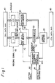
- FIG. 1 shows major elements of the microprocessor of the invention.
- the microprocessor includes a word data bus (or CPU bus) 10 as well as an address register 20, for example, a RAM address latching circuit, in which all the bit information constituting an address on the CPU bus are stored in response to an address latching signal.
- a word data bus or CPU bus
- an address register for example, a RAM address latching circuit, in which all the bit information constituting an address on the CPU bus are stored in response to an address latching signal.
- First and second byte data memories 70 and 80 comprise a word data memory, the second byte data memory receiving an address specifying signal which is formed of all the remaining bit information except the first bit sent from the address register 20.
- An incrementer 30 receives an address specifying signal in addition to the logical product of a word/byte specifying signal and the first bit from the address register 20.
- the incrementer 30 also provides as an address the logical addition of the logical product and an address specifying data to the first byte memory 70.
- a data memory input/output control signal generator 300 generates an input control signal which transfer selectively word writing data or byte writing data on the CPU bus 10 by higher and lower byte units to the first or second byte data memories 70 and 80.
- the generator 300 also produces an output control signal to transfer selectively data stored in the first and second byte data memories 70 and 80 to upper and lower bit lines of the CPU bus 10.
- An input circuit 400 selectively transfers the writing data on the CPU bus 10 by the upper and lower byte units to the first byte data memory 70 and to the second byte data memory 80.
- An output circuit 500 provides alternatel.y the data read from both the first byte data memory 70 or the second byte data memory 80 by the lower byte and upper byte unites.
- the CPU buses 0 through 15 transmit data processed in the CPU.
- the address register 20 stores as a data memory specifying address all the bit information on the CPU buses 0 to 15 with an occurrence of an address latching signal 21.
- the output signals Q0 to Q15 are, for example, a 16 bit information sent from the address register 20.
- the output signals 23 are all the remaining bit information except the first bit from the address register 20 and act as a base of address to specify the data memories 70 and 80.
- An output signal 24, or the first bit information Q0 from the address register 20 is supplied to the data memory input/output control signal generator 300 and may be used as a data input switching signal, a data memory data output signal, a data address generating signal, etc. for the data memory 70 and 80.
- An inverter gate 25 provides an inverted signal Q0 or 26 of an output signal Q0 or 24.
- the incrementer (or adder) 30 for example, a + 1 incrementer receives the signals Q0 through Q15 as well as a logical product signal (also referred to an incremental signal or a +1 addition signal) 42 of the output signal Q0 and a word/bite specifying signal 91 from the data memory input/output control signal generator 300.
- An address signal 31 is the output signals S0 through S14 from the incrementer 30 and specifies a lower byte data memory 70.
- a clock signal 90 is supplied to the data input/output control circuit 300 and is used as a synchronous clock for writing the memory data.
- a word/byte signal 91 specifies whether a data width for the data memory 70 or 80 used to process the CPU is in byte (ex. 8 bit) or word (ex. 16 bit).
- a writing signal 92 is provided to the data input/output control circuit 300 in a data writing operation to the data memory 70 or 80.
- a reading signal 93 is supplied to the data output circuit 500 in reading data out of the data memories 70 and 80
- a logical circuit 40 is, for example, a two input AND gate 41 and provides a +1 addition signal 42 to the incrementer 30 when it receives a word/byte signal 91 and an output signal Q0 (or 24) from the address register 20.
- a logical circuit 50 is formed of, for example, two-input OR gates 51 and 53 and outputs both a lower byte data memory specifying signal 52 and a upper byte data memory specifying signal 54 in response to the word/byte signal 91, the address register output Q0 and the inverter signal Q0.
- a logical circuit 60 is formed of, for example, two-input AND gates 61 and 63 and provides, in response to the signals 52 and 54 and a writing signal 92, a control signal 62 for inputting or writing data into the lower byte data memory 70 and a control signal 64 for inputting or writing data into the upper byte data memory 80.
- the first byte data memory 70 which is a lower byte data memory in this embodiment, is a part of the word data memory to store byte data.
- the second byte data memory 80 which is an upper byte data memory in this embodiment, is the remaining portion of the word data memory to store byte data.
- a logical circuit 71 is, for example, a two-input AND gate, and provides a writing signal to the lower byte data memory 70 when it receives a lower byte writing signal 62 and a clock signaL 90.
- a logical circuit 81 is of, for example, a two-input NAND gate. When both a writing signal 64 and a clock signal 90 are inputted to the circuit 81, a writing signal 82 is output to the second byte data memory 80.
- a logical circuit 100 inputs into the lower byte data memory 70 the lower byte data D0 to D7 selected among the data D0 to D15 written on the CPU bus 10.
- a three state circuit 101 to transmit the written data from the logical circuit 100 to the lower byte data memory bus 102.
- An inverter gate 45 switches the data input operation to the byte data memory and outputs an inverted signal 46 of a control signal 24 for specifying data output to a data memory.
- An arithmetic logical circuit 200 inputs to the upper byte data memory 80 the upper byte data D 8 to D15 by selectively switching the lower byte data and the upper byte data loaded on the CPU bus 10.
- a three state gate 201 transmits the written data from the circuit 200 to the upper byte data memory bus 202.
- the data switching circuit 400 comprises inverter gates 25 and 45, logical circuits 40, 50, 60, 71, 81, 100 and 200, and three state gates 101 and 201.
- the structure of the circuit 400 should not be restricted to the present embodiment and it will be possible to realize various modifications thereof.
- a three state gate 103 transmits the data read from the lower byte data memory 70 to the CPU buses 0 to 7.
- a three state gate 104 transmits the data read from the lower byte data memory 70 to the CPU buses 8 to 15.
- the inverter 45 outputs an inverted signal 46.
- a logical circuit 105 is, for example, a two-input NAND gate and provides a switching signal 106 to the three gate circuit 103 in response to both a reading signal 93 and the reversed signal 46 of the output signal Q0 from the address register 20.
- a two-input NAND gate circuit 107 as a logical circuit outputs a switching signal 108 to a three state gate 104 when it receives a reading signal 93 and an output signal Q0 of the address register 20.
- a three state gate 203 transmits the data read from the upper byte data memory 80 to the CPU buses 0 to 7.
- a three state gate 204 sends the data read from the upper byte data memory 80 to the CPU buses 8 to 15.
- a logical circuit 205 is, for example, a two input NAND gate and outputs a switching signal 206 to the three state gate 203 in response to a reading signal 93 and an inverted signal 46 of the output signal Q0 from the address register 20.
- a logical circuit 207 is, for example, a two input NAND gate and provides a switching signal 108 to the three state gate 204 when a reading signal 93 and the output signal Q0 of the address register 20 are input to the circuit 207.
- the data output switching circuit of the embodiment comprises the logical circuits 105, 107, 205 and 207, the three state circuits 103, 104, 203 and 204, and the inverter 45.
- the machine cycle A shows writing and reading operations to the data memory 70 or 80 of a word (for example, of a width of 16 bits) in which the head address is of odd number.
- the machine cycle B shows the writing and reading operations to the byte data memory 70 or 80 including word data (for example, a width of 16 bits) each in which the head address is of even number.
- the machine cycle C shows writing and reading operations to the byte data memory 70 or 80 including words (for example, a width of 8 bits) each in which the head address is of odd number.
- the machine cycle D shows the writing and reading operations to the byte data memory including bite data (for example, a width of 8 bits) each in which the head address is of odd number.
- Figures in the brackets of Figures 3A to 3C are reference numerals seen in Figures 2A and 2B.
- the machine cycle A seen in Figures 3A, 3B and 3C, is the operational mode that a word data (of a width of 16 bits) is written into or read out of an address in a head odd number address (for example, 0007H).
- the data memory specifying address 1110000000000000 is loaded to the CPU buses 0 to 15 , and the address register 20 outputs the address data 0007H when it receives an address latching signal 21 in a later portion of the state S0.
- the address register 20, for example, provides an address signal 23 which specifies the address 0003H of the upper byte data memory 80.
- the incrementer 30 produces an addition signal of an increment signal (or +1 addition signal) 42 and an address signal 23 to specify an address of the lower byte data memory 70.
- the logical circuit 40 since it receives both a word/bite specifying signal 91 of "1" and a signal 24 (or the first bit information Q0 of the address register 20) of "1", the logical circuit 40 produces an increment signal of a logical "1".
- the data 1111100010101001 (or 951FH in hexadecimal notation expressed from the upper bit order) for writing are loaded onto the CPU buses 0 to 15.
- the byte data at the head address take the lower place and the following byte data at the following address (or the head address plus 1) take the upper place.
- the data 951F consist of 95H taking the upper place and 1FH taking the lower place.
- the 1FH data are stored in the upper byte data memory 80 while the 95H data are stored in the lower byte data memory 70.
- the logical circuit 300 When the logical circuit 300 receives an data switching signal LA (or 24) of a "1" level in the later part of the state S0, the logical circuit 100 transfers the 95H data on the CPU buses 0 to 15 into the lower byte data memory 70 during the state S1. While the logical circuit 200, which receives an input switching signal HA (or 24) of a "1" level in the later part of the state S0, transfers the 1FH data on the CPU buses 0 to 15 to the upper byte data memory 80 during the state S1.
- the three state gates 101 and 201 load the 95H data on the CPU buses 8 to 15 into the lower byte memory buses 0 to 7 (or 102) and the 1F data of the CPU buses 0 to 7 into the upper byte data memory buses 0 to 7 (or 202), respectively.
- the 1FH data are stored in the 0007H address and the 95H data are stored in the 0008H address.
- the 1FH data are stored in the 0006 address of the upper byte data memory 80 and the 95H data are stored in the 0008 address of the lower byte data address 70.
- the reading signal 93 becomes a "1" level in the state S2
- the data which has been written in the state S1 in the address specified during the state S0 are loaded onto the CPU buses 0 to 15.
- the byte data at the head address takes the lower place and the byte data at the following address takes the upper place.
- the upper byte memory 80 provides the data onto the CPU buses 0 to 15 , when the reading data output signal OHB (or 208) is at a "1" level.
- the lower byte data memory 70 provides the data onto the CPU buses 8 to 15 when the data reading output signal OLB (or 108) becomes "1" level. Therefore, the CPU buses 0 to 15 are in 1111100010101001.
- the data memory specifying address 0000000000000000 are supplied onto the CPU buses 0 to 15 .
- the address register 20 receives the address latching signal 21 in the later part of the state S0 it outputs the data 0000H as an output signal 22. Also the data 0000H as an address signal 23 (or output bits Q1 to Q15 ) are output to specify the upper byte data memory 80.
- the incrementer 30 receives both an incremental signal (or +1 addition signal) 42 from the control signal generator 300 and an address signal 23 from the address register 20 to output an addition signal which is the address data for specifying the lower byte data memory 70.
- the word/byte specifying signal 91 is a "1" level and the first bit position information Q0 or the output signal 24 from the register 20 is in a "0" level, the incremental signal 42 to the incrementer 30 becomes a "0" level.
- the lower byte data memory 70 is specified to the same address 0000H as that of the upper byte data memory 80.
- the CPU buses 0 to 15 are supplied with the writing data 0101101011001010 (or 535AH in Hexadecimal notation expressed from the upper bit order).
- the lower byte data take the lower position and the upper byte data take the upper position.
- the logical circuit 100 receives a data switching signal LB or 46 of a "1" level, it transfers the data 5AH of the CPU data buses 0 to 7 to the lower byte memory buses 0 to 7 (or 102).
- the logical circuit 200 receives a data switching signal HB 46 of a "1" level, it sends the data 53H of the CPU data buses 8 to 15 into the upper byte memory bus 0 to 7 (202).
- the 5AH data are stored in the address 0001H while the 53H data are stored in the address 0001H.
- the 5AH data are stored in the address 000H of the lower byte data memory 70, while the 53H data are stored in the address 0000H of the upper byte data memory 80.
- the content of the lower byte data memory 70 occupies the lower position of the word specifying address, while the content of the upper byte data memory 80 occupies the upper position thereof.
- the lower byte data memory 70 provides readout data onto the CPU data buses 0 to 7.
- the data output signal OAH (or 206) is in "1”
- the upper byte data memory 80 provides readout data onto the CPU data buses 8 to 15. Therefore, the CPU data buses 0 to 15 are in 0101101011001010.
- the address data 1001000000000000 are provided onto the CPU data buses 0 to 15 to specify the data memory.
- the address register 20 receives an address latching signal 21 during the later part of the state S0, it outputs data 0009H.
- the address signal 23 specifies the address 0004H which is a specifying address for the upper byte data memory 80.
- the specifying address for the lower byte data memory 70 is an addition value of the increment signal (or +1 addition signal) 42 and the address signal 23.
- the word/byte specifying signal 91 is in "0" to perform a byte processing and the incrementer 30 receives an increment signal 42 of "0". For this reason, the lower byte data memory 70 is specified to the same address of 0004H as that of the upper byte data memory 80.
- the CPU data buses 0 to 15 are provided with the writing data of 0101010111111111 (or 0FFAAHH in Hexadecimal notation).
- the data OFFAAH on the CPU data buses 8 to 15 are "1''s which are obtained by precharging the CPU data buses 0 to 15.
- byte data are written into the byte data memory 70 or 80, it is stored in only a specified byte data memory address, but an unspecified byte data memory address.
- the logical circuit 50 receives a word/byte specifying signal 91 of "0" the first bit signal Q0 (or 24) of "1" from the address register 20 becomes valid.
- the OR gate 53 receives the first bit signal Q0 and the output signal 54 selects the upper byte data memory 80.
- the logical circuit 200 also receives the bit signal 24 of "1" so that the OAAH data on the CPU data buses 0 to 7 are loaded onto the upper byte data memory buses 0 to 7 (or 202).
- the 0AAH data are stored in the byte address 0009H and the OAAH data are stored in the upper byte date memory 80.
- the byte data in a specified address are read out onto the CPU data buses 0 to 7 and the content in a byte specifying address of the byte data memory 70 are read out onto the CPU data buses 8 to 15 .
- the three state gate 208 receives a data output signal OHB (or 208) in the state S2
- the upper byte data memory 80 outputs the read data onto the CPU data buses 0 to 7.
- the three state gate 108 receives a data output signal OLB (or 108)
- the lower byte data memory 70 provides the read data onto the CPU data buses 8 to 15 .
- the bit information on the CPU data buses 0 to 15 becomes 0101010110101001.
- the address register 20 When the address data 0110000000000000 occur on the CPU data buses 0 to 15 in the state S0 of the machine cycle C and an address latching signal 21 is input to the address register 20 in the later part of the stated S0, the address register 20 provides the data 0006H.
- the address signal 23 represents the data 0003H and specifies the upper byte data memory 80.
- the addressing for the lower byte data memory 70 is determined an addition value of an increment signal 42 and an address signal 23. In this case, the word/byte signal is "0" because of the byte processing so that the address specifying the lower byte data memory 70 is 0003H which is the same as that of upper byte data memory 80.
- the writing data 10100101111111111 which is referred to OFFA5H in Hexadecimal notation are supplied onto the CPU data buses 0 to 15.
- the data on the CPU data buses 0 to 15 are "1" levels which are obtained by precharging the data buses 0 to 15 .
- the data are stored into the byte data memory 70 or 80 corresponding to a specified address and new data are not stored into the unspecified byte data memory 80 or 70.
- the output signal Q0 becomes valid since the data memory selection circuit 50 receives a word/bite specifying signal 91 of "0".
- the gate 51 outputs a signal Q0 of "1" to select the lower byte data memory 70.
- the gate 53 outputs a signal of "0" but it does not select the upper byte data memory 80.
- the logical circuit 100 transfers through the three state gate 101 the data on the CPU data buses 0 to 7 selected by the selection signal 46 from the inverter 45 to the bus 102 of the lower byte data memory 70.
- the A5H data are stored into the byte address 0006 which corresponds to the word address of 0006H in the lower byte data memory 70.
- the CPU data buses 0 to 7 receives the byte data read from a specified address while the CPU data buses 8 to 15 receives the content from a word address as a byte specifying address of the byte data memory 70 or 80. Therefore, the data output signal OLA (or 106) becomes "l”in the state S2 so that the data read out onto the CPU data buses 0 to 7. Then the data output signal OHA (or 206) changes into "1", the upper byte data memory 80 outputs the read data onto the CPU data buses 8 to 15. As a result, the CPU data buses 0 to 15 are in 1010010111111000.
- the microprocessor according to the present invention includes a word data memory which comprises an upper byte data memory and an lower byte data memory.
- the improved microprocessor also has an incrementer which produces an address for specifying the lower byte data memory and which enable an access operation by only one time addressing.
- the microprocessor of this invention is applicable to CPU memory systems which require high speed processing.
Landscapes
- Engineering & Computer Science (AREA)
- Theoretical Computer Science (AREA)
- Physics & Mathematics (AREA)
- General Engineering & Computer Science (AREA)
- General Physics & Mathematics (AREA)
- Bus Control (AREA)
- Microcomputers (AREA)
- Memory System (AREA)
Abstract
Description
- This invention relates to a microprocessor, and particularly to a central processing unit (CPU) for use in a microcomputer having a word data memory.
- In prior art microprocessors, in order to improve the access processing to a CPU, the word data memory may be stored with program data arranged in a word order that lower bytes or upper bytes are stored at even number addresses while upper bytes or lower bytes are stored at odd number addresses
- However, when the top lower byte (or the top upper byte) of data is stored in an odd number address, the CPU has to perform addressing twice and to access separately the lower bytes and the upper bytes. The two time memory accessing results in slow process operation.
- The object of the present invention provides an improved microprocessor which make it possible to arrange program data without taking account of memory address.
- The further object of the present invention provides an improved microprocessor having word data memories which make high rate processing possible.
- A microprocessor having a word data memory according to the present invention is characterized in that a CPU data bus, an address register, an incrementer, first and second byte data memories, a data input switching circuit and a data output switching circuit. The CPU data bus has higher bit lines and lower bit lines. The address register stores all the bit information of an address on the CPU data bus in response to an address latching signal. The incrementer receives an address specifying data as well as a logical product of a word/byte specifying signal and the first bit information from the address register, the address specifying data consist of all the remaining bits except the first bit from the address register. The first byte data memory forms a portion of the word data memory to provide a logical addition of the logical product from the incrementer and the address specifying signal. The second byte data memory forms the remaining portion of the word data memory to receive the address specifying output which consists of all the remaining bits except the first bit from the address register. The data input switching circuit selectively transfers into the first and second byte data memories word writing data and byte writing data on the CPU data bus by higher bit units and lower bit units. The data output switching circuit selectively provides data of the first and second byte data memories onto the higher bit lines and the lower bit lines.
- The objects stated above and other objects of the invention are set forth more particularly in the following detailed description and in the accompanying drawings, of which;
- Figure 1 is a block diagram showing general features of a microprocessor according to the present invention;
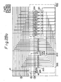
- Figures 2A and 2B are a detailed logic diagram showing the microprocessor of Figures 1A and 1B; and
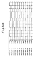
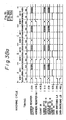
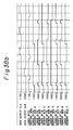
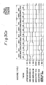
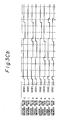
- Figure 3A, 3B and 3C are timing charts for explaining operation of the microprocessor shown in Figures 2A and 2B.
- An embodiment according to the present invention will be explained with reference to the accompanying drawings.
- Figure 1 shows major elements of the microprocessor of the invention.
- In Figure 1, the microprocessor includes a word data bus (or CPU bus) 10 as well as an
address register 20, for example, a RAM address latching circuit, in which all the bit information constituting an address on the CPU bus are stored in response to an address latching signal. - First and second
byte data memories address register 20. - An
incrementer 30 receives an address specifying signal in addition to the logical product of a word/byte specifying signal and the first bit from theaddress register 20. Theincrementer 30 also provides as an address the logical addition of the logical product and an address specifying data to thefirst byte memory 70. - A data memory input/output
control signal generator 300 generates an input control signal which transfer selectively word writing data or byte writing data on theCPU bus 10 by higher and lower byte units to the first or secondbyte data memories generator 300 also produces an output control signal to transfer selectively data stored in the first and secondbyte data memories CPU bus 10. - An
input circuit 400 selectively transfers the writing data on theCPU bus 10 by the upper and lower byte units to the firstbyte data memory 70 and to the secondbyte data memory 80. - An
output circuit 500 provides alternatel.y the data read from both the firstbyte data memory 70 or the secondbyte data memory 80 by the lower byte and upper byte unites. - A detailed circuit configuration of a microprocessor according to the present invention will be described with reference to Figures 2A and 2B. In Figure 1 and Figures 2A and 2B, the same numerals represent the same elements.
- In Figures 2A and 2B, the
CPU buses 0 through 15 transmit data processed in the CPU. The address register 20 stores as a data memory specifying address all the bit information on theCPU buses 0 to 15 with an occurrence of an address latching signal 21. The output signals Q₀ to Q₁₅ are, for example, a 16 bit information sent from theaddress register 20. Theoutput signals 23 are all the remaining bit information except the first bit from theaddress register 20 and act as a base of address to specify thedata memories output signal 24, or the first bit information Q₀ from theaddress register 20, is supplied to the data memory input/outputcontrol signal generator 300 and may be used as a data input switching signal, a data memory data output signal, a data address generating signal, etc. for thedata memory inverter gate 25 provides an inverted signal Q₀ or 26 of an output signal Q₀ or 24. - The incrementer (or adder) 30 for example, a + 1 incrementer receives the signals Q₀ through Q₁₅ as well as a logical product signal (also referred to an incremental signal or a +1 addition signal) 42 of the output signal Q₀ and a word/
bite specifying signal 91 from the data memory input/outputcontrol signal generator 300. Anaddress signal 31 is the output signals S₀ through S₁₄ from theincrementer 30 and specifies a lowerbyte data memory 70. Aclock signal 90 is supplied to the data input/output control circuit 300 and is used as a synchronous clock for writing the memory data. A word/byte signal 91 specifies whether a data width for thedata memory writing signal 92 is provided to the data input/output control circuit 300 in a data writing operation to thedata memory reading signal 93 is supplied to thedata output circuit 500 in reading data out of thedata memories - In the input/output
control signal generator 300, alogical circuit 40 is, for example, a two input AND gate 41 and provides a +1addition signal 42 to theincrementer 30 when it receives a word/byte signal 91 and an output signal Q₀ (or 24) from theaddress register 20. Alogical circuit 50 is formed of, for example, two-input ORgates memory specifying signal 52 and a upper byte datamemory specifying signal 54 in response to the word/byte signal 91, the address register output Q₀ and the inverter signal Q₀. A logical circuit 60 is formed of, for example, two-input AND gates 61 and 63 and provides, in response to thesignals writing signal 92, a control signal 62 for inputting or writing data into the lowerbyte data memory 70 and acontrol signal 64 for inputting or writing data into the upperbyte data memory 80. - The first
byte data memory 70, which is a lower byte data memory in this embodiment, is a part of the word data memory to store byte data. The secondbyte data memory 80, which is an upper byte data memory in this embodiment, is the remaining portion of the word data memory to store byte data. Alogical circuit 71 is, for example, a two-input AND gate, and provides a writing signal to the lowerbyte data memory 70 when it receives a lower byte writing signal 62 and aclock signaL 90. A logical circuit 81 is of, for example, a two-input NAND gate. When both awriting signal 64 and aclock signal 90 are inputted to the circuit 81, awriting signal 82 is output to the secondbyte data memory 80. - In a
data input circuit 400, alogical circuit 100 inputs into the lowerbyte data memory 70 the lower byte data D₀ to D₇ selected among the data D₀ to D₁₅ written on theCPU bus 10. A three state circuit 101 to transmit the written data from thelogical circuit 100 to the lower bytedata memory bus 102. An inverter gate 45 switches the data input operation to the byte data memory and outputs an invertedsignal 46 of acontrol signal 24 for specifying data output to a data memory. - An arithmetic
logical circuit 200 inputs to the upperbyte data memory 80 the upper byte data D₈ to D₁₅ by selectively switching the lower byte data and the upper byte data loaded on theCPU bus 10. A threestate gate 201 transmits the written data from thecircuit 200 to the upper bytedata memory bus 202. - As seen from the above explanation, the
data switching circuit 400 comprisesinverter gates 25 and 45,logical circuits state gates 101 and 201. However, the structure of thecircuit 400 should not be restricted to the present embodiment and it will be possible to realize various modifications thereof. - Next, a data
output switching circuit 500 will be explained. - A three
state gate 103 transmits the data read from the lowerbyte data memory 70 to theCPU buses 0 to 7. A threestate gate 104 transmits the data read from the lowerbyte data memory 70 to theCPU buses 8 to 15. The inverter 45 outputs aninverted signal 46. - A
logical circuit 105 is, for example, a two-input NAND gate and provides aswitching signal 106 to the threegate circuit 103 in response to both areading signal 93 and the reversedsignal 46 of the output signal Q₀ from theaddress register 20. - A two-input
NAND gate circuit 107 as a logical circuit outputs aswitching signal 108 to a threestate gate 104 when it receives areading signal 93 and an output signal Q₀ of theaddress register 20. - A three
state gate 203 transmits the data read from the upperbyte data memory 80 to theCPU buses 0 to 7. A threestate gate 204 sends the data read from the upperbyte data memory 80 to theCPU buses 8 to 15. - A
logical circuit 205 is, for example, a two input NAND gate and outputs a switching signal 206 to the threestate gate 203 in response to areading signal 93 and aninverted signal 46 of the output signal Q₀ from theaddress register 20. Alogical circuit 207 is, for example, a two input NAND gate and provides aswitching signal 108 to the threestate gate 204 when areading signal 93 and the output signal Q₀ of theaddress register 20 are input to thecircuit 207. - As understood the above description, the data output switching circuit of the embodiment comprises the
logical circuits state circuits - An operation of the embodiment according to the present invention will be explained with reference to timing charts shown in Figures 3A to 3C.
- Figures 3A through 3C include letters A, B and C showing machine cycles, W/B=1 meaning word selection, and W/B=0 meaning byte selection. A0=1 means odd number address selecting operation and A0=0 means even number address selection operation and S0, S1 and S2 represent timings in machine cycles of CPU. For example, the machine cycle A shows writing and reading operations to the
data memory byte data memory byte data memory - Now,let us assume that the data memories stored data seen in the following Table I.

- The machine cycle A seen in Figures 3A, 3B and 3C, is the operational mode that a word data (of a width of 16 bits) is written into or read out of an address in a head odd number address (for example, 0007H).
- In the state S₀, the data memory specifying address 1110000000000000 is loaded to the
CPU buses 0 to 15 , and theaddress register 20 outputs theaddress data 0007H when it receives an address latching signal 21 in a later portion of the state S₀. Theaddress register 20, for example, provides anaddress signal 23 which specifies theaddress 0003H of the upperbyte data memory 80. Theincrementer 30 produces an addition signal of an increment signal (or +1 addition signal) 42 and anaddress signal 23 to specify an address of the lowerbyte data memory 70. In this case, since it receives both a word/bite specifying signal 91 of "1" and a signal 24 (or the first bit information Q₀ of the address register 20) of "1", thelogical circuit 40 produces an increment signal of a logical "1". Theincrementer 30 generates to the lowerbyte data memory 70 an address of the +1 addition signal plus the address for the upper byte data memory being the remaining bit information Q₁ to Q₁₅. Therefore, the lowerbyte data memory 70 is specified to the address of 1 + 0003H = 0004H. - In the state S₁, the data 1111100010101001 (or 951FH in hexadecimal notation expressed from the upper bit order) for writing are loaded onto the
CPU buses 0 to 15. In the word data preceded by an odd number address, the byte data at the head address take the lower place and the following byte data at the following address (or the head address plus 1) take the upper place. For example, the data 951F consist of 95H taking the upper place and 1FH taking the lower place. The 1FH data are stored in the upperbyte data memory 80 while the 95H data are stored in the lowerbyte data memory 70. When thelogical circuit 300 receives an data switching signal LA (or 24) of a "1" level in the later part of the state S₀, thelogical circuit 100 transfers the 95H data on theCPU buses 0 to 15 into the lowerbyte data memory 70 during the state S₁. While thelogical circuit 200, which receives an input switching signal HA (or 24) of a "1" level in the later part of the state S₀, transfers the 1FH data on theCPU buses 0 to 15 to the upperbyte data memory 80 during the state S₁. When the gate switching signals 62 and 64 become a "1" level during the state S₁, the threestate gates 101 and 201 load the 95H data on theCPU buses 8 to 15 into the lowerbyte memory buses 0 to 7 (or 102) and the 1F data of theCPU buses 0 to 7 into the upper bytedata memory buses 0 to 7 (or 202), respectively. - When the
clock signal 90 turns "0" to "1" in the later part of the state S₁ and both the lower byte writing signal WML (or 72) and the upper byte writing signal WMH (or 82) turns "1" to "0", the data are stored in the arrangement shown in the following Table II.TABLE II Byte Address Byte Data Word Address Upper Byte Data Lower Byte Data 0000H 00H 0000H 00H OOH 0001H 00H 0002H 00H 0002H 00H OOH 0003H 00H 0004H 00H 0004H 00H OOH 0005H 00H 0006H 00H 0006H *1FH OOH 0007H *1FH 0008H *95H 0008H OOH *95H 0009H * Written data shown in this present embodiment. - As seen in the Table II, in byte address arrangement of the 951FH data, the 1FH data are stored in the 0007H address and the 95H data are stored in the 0008H address. On the other hand, in word address arrangement of the 951FH data, the 1FH data are stored in the 0006 address of the upper
byte data memory 80 and the 95H data are stored in the 0008 address of the lowerbyte data address 70. - When the
reading signal 93 becomes a "1" level in the state S₂, the data which has been written in the state S₁ in the address specified during the state S₀ are loaded onto theCPU buses 0 to 15. In case word data (of 16 bits) of a head odd number address are read, the byte data at the head address takes the lower place and the byte data at the following address takes the upper place. During the state S₂, theupper byte memory 80 provides the data onto theCPU buses 0 to 15 , when the reading data output signal OHB (or 208) is at a "1" level. The lowerbyte data memory 70 provides the data onto theCPU buses 8 to 15 when the data reading output signal OLB (or 108) becomes "1" level. Therefore, theCPU buses 0 to 15 are in 1111100010101001. - Next, an operation for reading and writing word data (of 16 bits) into an address preceded by even number address during the machine cycle B will be explained.
- In the state S₀ of the machine cycle B, the data memory specifying address 0000000000000000 are supplied onto the
CPU buses 0 to 15 . When theaddress register 20 receives the address latching signal 21 in the later part of the state S₀ it outputs thedata 0000H as an output signal 22. Also thedata 0000H as an address signal 23 (or output bits Q₁ to Q₁₅ ) are output to specify the upperbyte data memory 80. Theincrementer 30 receives both an incremental signal (or +1 addition signal) 42 from thecontrol signal generator 300 and anaddress signal 23 from theaddress register 20 to output an addition signal which is the address data for specifying the lowerbyte data memory 70. When the word/byte specifying signal 91 is a "1" level and the first bit position information Q₀ or theoutput signal 24 from theregister 20 is in a "0" level, theincremental signal 42 to theincrementer 30 becomes a "0" level. As a result, the lowerbyte data memory 70 is specified to thesame address 0000H as that of the upperbyte data memory 80. - In the state S₁, the
CPU buses 0 to 15 are supplied with the writing data 0101101011001010 (or 535AH in Hexadecimal notation expressed from the upper bit order). - In the word data preceded by even addresses, the lower byte data take the lower position and the upper byte data take the upper position. When the
logical circuit 100 receives a data switching signal LB or 46 of a "1" level, it transfers the data 5AH of theCPU data buses 0 to 7 to the lowerbyte memory buses 0 to 7 (or 102). On the other hand, thelogical circuit 200 receives a data switchingsignal HB 46 of a "1" level, it sends the data 53H of theCPU data buses 8 to 15 into the upperbyte memory bus 0 to 7 (202). - In the later part of the state S₁, when the clock signal turns "0" to "1" and the lower and upper byte data memory writing signals WML (or 72) and WMH (or 82) turn "1" to "0", respectively, the data are written in the
byte data memories TABLE III Byte Address Byte Data Word Address Upper Byte Data Lower Byte Data 0000H * 5AH 0000H *53H *5AH 0001H *53H 0002H 00H 0002H 00H OOH 0003H 00H 0004H 00H 0004H 00H OOH 0005H 00H 0006H 00H 0006H 1FH OOH 0007H 1FH 0008H 95H 0008H OOH 95H 0009H 00H *Written data shown in this present invention. - As seen in the Table III, in byte address arrangement of the 535AH data, the 5AH data are stored in the address 0001H while the 53H data are stored in the address 0001H. In word address arrangement of the 535AH data, the 5AH data are stored in the address 000H of the lower
byte data memory 70, while the 53H data are stored in theaddress 0000H of the upperbyte data memory 80. - In the state S₂, when the
reading signal 93 turns to "1", the data written during the state S₁ into the address specified during the state S₀ are loaded onto theCPU data buses 0 to 15. - In case word data (of 16 bits) of the head even number address are read out, the content of the lower
byte data memory 70 occupies the lower position of the word specifying address, while the content of the upperbyte data memory 80 occupies the upper position thereof. In the state S₂, when the data output signal OLA (or 106) is in "1", the lowerbyte data memory 70 provides readout data onto theCPU data buses 0 to 7. Since the data output signal OAH (or 206) is in "1", the upperbyte data memory 80 provides readout data onto theCPU data buses 8 to 15. Therefore, theCPU data buses 0 to 15 are in 0101101011001010. - Next, it will be expressed that byte (8 bits) data are written into a head odd number address in the machine cycle C.
- In the state S₀ of the machine cycle C, the address data 1001000000000000 are provided onto the
CPU data buses 0 to 15 to specify the data memory. When theaddress register 20 receives an address latching signal 21 during the later part of the state S₀, it outputs data 0009H. Theaddress signal 23 specifies theaddress 0004H which is a specifying address for the upperbyte data memory 80. The specifying address for the lowerbyte data memory 70 is an addition value of the increment signal (or +1 addition signal) 42 and theaddress signal 23. The word/byte specifying signal 91 is in "0" to perform a byte processing and theincrementer 30 receives anincrement signal 42 of "0". For this reason, the lowerbyte data memory 70 is specified to the same address of 0004H as that of the upperbyte data memory 80. - In the state S₁, the
CPU data buses 0 to 15 are provided with the writing data of 0101010111111111 (or 0FFAAHH in Hexadecimal notation).
In this case, the data OFFAAH on theCPU data buses 8 to 15 are "1''s which are obtained by precharging theCPU data buses 0 to 15. When byte data are written into thebyte data memory logical circuit 50 receives a word/byte specifying signal 91 of "0" the first bit signal Q₀ (or 24) of "1" from theaddress register 20 becomes valid. TheOR gate 53 receives the first bit signal Q₀ and theoutput signal 54 selects the upperbyte data memory 80. Thelogical circuit 200 also receives thebit signal 24 of "1" so that the OAAH data on theCPU data buses 0 to 7 are loaded onto the upper bytedata memory buses 0 to 7 (or 202). - In the later part of the state S₁, when the
clock signal 90 turns "0" to "1", the writing signal WMH (or 82) goes "1" to "0". The data are written into the upperbyte data memory 80 in the arrangement as seen in the following Table IV.TABLE IV Byte Address Byte Data Word Address Upper Byte Data Lower Byte Data 0000H 5AH 0000H 53H 5AH 0001H 53H 0002H 00H 0002H 00H OOH 0003H 00H 0004H 00H 0004H 00H OOH 0005H 00H 0006H 00H 0006H 1FH OOH 0007H 1FH 0008H 95H 0008H *AAH 95H 0009H *AAH * Written data shown in this present invention. - As seen in the Table IV, the 0AAH data are stored in the byte address 0009H and the OAAH data are stored in the upper
byte date memory 80. - In the state S₂, when the
reading signal 93 turns to "1", the data written during the state S₁ into the address specified during the state S₀ are read out to theCPU data buses 0 to 7 . - In a byte data reading operation, the byte data in a specified address are read out onto the
CPU data buses 0 to 7 and the content in a byte specifying address of thebyte data memory 70 are read out onto theCPU data buses 8 to 15 . When the threestate gate 208 receives a data output signal OHB (or 208) in the state S₂, the upperbyte data memory 80 outputs the read data onto theCPU data buses 0 to 7. When the threestate gate 108 receives a data output signal OLB (or 108), the lowerbyte data memory 70 provides the read data onto theCPU data buses 8 to 15 . As a result, the bit information on theCPU data buses 0 to 15 becomes 0101010110101001. - Next, the reading and writing operations of byte (8 bits) data into an address preceded by an even address will be explained based on the machine cycle D.
- When the address data 0110000000000000 occur on the
CPU data buses 0 to 15 in the state S₀ of the machine cycle C and an address latching signal 21 is input to theaddress register 20 in the later part of the stated S₀, theaddress register 20 provides the data 0006H. Theaddress signal 23 represents thedata 0003H and specifies the upperbyte data memory 80. The addressing for the lowerbyte data memory 70 is determined an addition value of anincrement signal 42 and anaddress signal 23. In this case, the word/byte signal is "0" because of the byte processing so that the address specifying the lowerbyte data memory 70 is 0003H which is the same as that of upperbyte data memory 80. - In the state S₁, the writing data 10100101111111111 which is referred to OFFA5H in Hexadecimal notation are supplied onto the
CPU data buses 0 to 15. In this case, the data on theCPU data buses 0 to 15 are "1" levels which are obtained by precharging thedata buses 0 to 15 . - In the byte data writing operation, the data are stored into the
byte data memory byte data memory memory selection circuit 50 receives a word/bite specifying signal 91 of "0". Thegate 51 outputs a signal Q₀ of "1" to select the lowerbyte data memory 70. On the other hand, thegate 53 outputs a signal of "0" but it does not select the upperbyte data memory 80. - In the state S₁, the
logical circuit 100 transfers through the three state gate 101 the data on theCPU data buses 0 to 7 selected by theselection signal 46 from the inverter 45 to thebus 102 of the lowerbyte data memory 70. - In the later part of the state S₁, when the clock signal changes from "1" to "0" and then the writing signal WML (or 72) changes from "1" to "0", the data in arrangement seen in the following Table V are stored in the lower
byte data memory 70.TABLE V Byte Address Byte Data Word Address Upper Byte Data Lower Byte Data 0000 5AH 0000H 53H 5AH 0001 53H 0002 00H 0002H 00H OOH 0003 00H 0004 00H 0004H 00H OOH 0005 00H 0006 *A5H 0006H 1FH *A5H 0007 1FH 0008 95H 0008H AAH 95H 0009 AAH * Written data shown in this present invention. - As seen from the Table V, the A5H data are stored into the byte address 0006 which corresponds to the word address of 0006H in the lower
byte data memory 70. - In the state S₂, when the
reading signal 93 is "1", the data written during the state S₁ in the address specified during the state S₀ are read onto theCPU data buses 0 to 7. - In the byte data reading operation, the
CPU data buses 0 to 7 receives the byte data read from a specified address while theCPU data buses 8 to 15 receives the content from a word address as a byte specifying address of thebyte data memory CPU data buses 0 to 7. Then the data output signal OHA (or 206) changes into "1", the upperbyte data memory 80 outputs the read data onto theCPU data buses 8 to 15. As a result, theCPU data buses 0 to 15 are in 1010010111111000. - As described above, the microprocessor according to the present invention includes a word data memory which comprises an upper byte data memory and an lower byte data memory. The improved microprocessor also has an incrementer which produces an address for specifying the lower byte data memory and which enable an access operation by only one time addressing. The microprocessor of this invention is applicable to CPU memory systems which require high speed processing.
Claims (4)
a CPU data bus having higher bit lines and lower bit lines;
an address register for storing all the bit information of an address on the CPU data bus in response to an address latching signal;
an incrementer for receiving an address specifying data as well as a logical product of a word/byte specifying signal and the first bit information from the address register, the address specifying data consist of all the remaining bits except the first bit from the address register;
first byte data memory means forming a portion of the word data memory for providing a logical addition of the logical product from the incrementer and the address specifying signal;
second byte data memory means forming the remaining portion of the word data memory for receiving the address specifying output which consists of all the remaining bits except the first bit from the address register;
data input switching means for selectively transferring into the first and second byte data memory means word writing data and byte writing data on the CPU data bus by higher bit unit and lower bit unit; and
data output switching means from selectively providing data of the first and second byte data memory means onto the higher bit lines and the lower bit lines.
wherein the data input switching means comprises a first logical circuit connected to the CPU data bus for selectively transmitting the lower byte data of the data loaded on the CPU data bus, first gating means connected to the first logical circuit for transmitting the lower byte data from the first logical circuit to the lower byte data memory means, a second logical circuit connected to the CPU data bus for transmitting the upper byte data of the data loaded on the CPU data bus, and second gating means connected to the second logical circuit to the upper byte data memory means for selectively transmitting the upper byte data from the second logical circuit to the CPU byte data means.
wherein the data output switching means comprises a first gating means connected to the lower byte data memory means for transmitting the lower byte data to the CPU data bus, and a second gating means connected to the upper byte data memory means for transmitting the upper byte data to the CPU data bus.
further comprising an input/output control signal generator connected to the first and second byte data memories for generating an input control signal which transfers selectively word writing data or byte writing data on the CPU data bus by higher and lower byte units to the first and second byte data memories.
Applications Claiming Priority (2)
| Application Number | Priority Date | Filing Date | Title |
|---|---|---|---|
| JP335678/87 | 1987-12-29 | ||
| JP62335678A JPH01175649A (en) | 1987-12-29 | 1987-12-29 | Micro processor |
Publications (3)
| Publication Number | Publication Date |
|---|---|
| EP0322880A2 true EP0322880A2 (en) | 1989-07-05 |
| EP0322880A3 EP0322880A3 (en) | 1990-08-29 |
| EP0322880B1 EP0322880B1 (en) | 1996-05-15 |
Family
ID=18291282
Family Applications (1)
| Application Number | Title | Priority Date | Filing Date |
|---|---|---|---|
| EP88121772A Expired - Lifetime EP0322880B1 (en) | 1987-12-29 | 1988-12-28 | Microprocessor having a word data memory |
Country Status (4)
| Country | Link |
|---|---|
| US (1) | US5101343A (en) |
| EP (1) | EP0322880B1 (en) |
| JP (1) | JPH01175649A (en) |
| DE (1) | DE3855298T2 (en) |
Cited By (3)
| Publication number | Priority date | Publication date | Assignee | Title |
|---|---|---|---|---|
| EP0684559A1 (en) * | 1994-05-23 | 1995-11-29 | Advanced Micro Devices, Inc. | Processing unit with byte-alignment mechanism |
| EP1324202A3 (en) * | 2001-12-28 | 2004-01-02 | Fujitsu Limited | Device and method for information processing |
| FR2884002A1 (en) * | 2005-04-01 | 2006-10-06 | St Microelectronics Sa | Bit symbol addressing method for use in memory bank of processing device, involves shifting symbol bits during reading or writing operation of symbols in memory bank based on value of pointer in read or written bit word |
Family Cites Families (8)
| Publication number | Priority date | Publication date | Assignee | Title |
|---|---|---|---|---|
| JPS5834836B2 (en) * | 1975-12-29 | 1983-07-29 | 株式会社日立製作所 | data |
| US4171536A (en) * | 1976-05-03 | 1979-10-16 | International Business Machines Corporation | Microprocessor system |
| JPS5438724A (en) * | 1977-09-02 | 1979-03-23 | Hitachi Ltd | Display unit |
| US4151327A (en) * | 1978-02-24 | 1979-04-24 | Lawton William R | Complex amine/silane treated cellulosic materials |
| JPS5727543A (en) * | 1980-07-24 | 1982-02-13 | Mitsubishi Electric Corp | Picture tube device |
| US4432055A (en) * | 1981-09-29 | 1984-02-14 | Honeywell Information Systems Inc. | Sequential word aligned addressing apparatus |
| US4604695A (en) * | 1983-09-30 | 1986-08-05 | Honeywell Information Systems Inc. | Nibble and word addressable memory arrangement |
| US4777591A (en) * | 1984-01-03 | 1988-10-11 | Texas Instruments Incorporated | Microprocessor with integrated CPU, RAM, timer, and bus arbiter for data communications systems |
-
1987
- 1987-12-29 JP JP62335678A patent/JPH01175649A/en active Pending
-
1988
- 1988-12-20 US US07/288,072 patent/US5101343A/en not_active Expired - Lifetime
- 1988-12-28 EP EP88121772A patent/EP0322880B1/en not_active Expired - Lifetime
- 1988-12-28 DE DE3855298T patent/DE3855298T2/en not_active Expired - Fee Related
Cited By (5)
| Publication number | Priority date | Publication date | Assignee | Title |
|---|---|---|---|---|
| EP0684559A1 (en) * | 1994-05-23 | 1995-11-29 | Advanced Micro Devices, Inc. | Processing unit with byte-alignment mechanism |
| US5566312A (en) * | 1994-05-23 | 1996-10-15 | Advanced Micro Devices | Processimg unit with programmable mis-aligned byte addressing |
| EP1324202A3 (en) * | 2001-12-28 | 2004-01-02 | Fujitsu Limited | Device and method for information processing |
| US6931508B2 (en) | 2001-12-28 | 2005-08-16 | Fujitsu Limited | Device and method for information processing |
| FR2884002A1 (en) * | 2005-04-01 | 2006-10-06 | St Microelectronics Sa | Bit symbol addressing method for use in memory bank of processing device, involves shifting symbol bits during reading or writing operation of symbols in memory bank based on value of pointer in read or written bit word |
Also Published As
| Publication number | Publication date |
|---|---|
| DE3855298D1 (en) | 1996-06-20 |
| EP0322880A3 (en) | 1990-08-29 |
| US5101343A (en) | 1992-03-31 |
| EP0322880B1 (en) | 1996-05-15 |
| DE3855298T2 (en) | 1997-01-23 |
| JPH01175649A (en) | 1989-07-12 |
Similar Documents
| Publication | Publication Date | Title |
|---|---|---|
| US4694394A (en) | Microprocessor system having a multiplexed address/data bus which communicates with a plurality of memory and input/output devices including TTL output gates | |
| US4163280A (en) | Address management system | |
| US5345573A (en) | High speed burst read address generation with high speed transfer | |
| US4482952A (en) | Virtual addressing system using page field comparisons to selectively validate cache buffer data on read main memory data | |
| EP0192202A2 (en) | Memory system including simplified high-speed data cache | |
| JPH10500790A (en) | Efficient addressing of large memories | |
| US4473877A (en) | Parasitic memory expansion for computers | |
| GB1449229A (en) | Data processing system and method therefor | |
| US4344130A (en) | Apparatus to execute DMA transfer between computing devices using a block move instruction | |
| EP0282248B1 (en) | Block access system using cache memory | |
| EP0315194A2 (en) | Microcomputer capable of accessing continuous addresses for a short time | |
| US5822762A (en) | Information processing device with decision circuits and partitioned address areas | |
| EP0322880B1 (en) | Microprocessor having a word data memory | |
| US4831513A (en) | Memory initialization system | |
| EP0334103B1 (en) | Data processing unit having a bypass circuit | |
| US5179676A (en) | Address selection circuit including address counters for performing address selection | |
| EP0057096A2 (en) | Information processing unit | |
| US5101376A (en) | Integrated microprocessor with associative memory device | |
| US4959778A (en) | Address space switching apparatus | |
| JPH0855471A (en) | Synchronous semiconductor memory device | |
| KR0184633B1 (en) | Cfiucore | |
| EP0114683B1 (en) | Arithmetic unit | |
| EP0352806A2 (en) | Cache memory and access controller using such memory | |
| US4561071A (en) | Storage system having buffer storage | |
| EP0108647A2 (en) | Data processing apparatus |
Legal Events
| Date | Code | Title | Description |
|---|---|---|---|
| PUAI | Public reference made under article 153(3) epc to a published international application that has entered the european phase |
Free format text: ORIGINAL CODE: 0009012 |
|
| AK | Designated contracting states |
Kind code of ref document: A2 Designated state(s): DE FR GB |
|
| PUAL | Search report despatched |
Free format text: ORIGINAL CODE: 0009013 |
|
| AK | Designated contracting states |
Kind code of ref document: A3 Designated state(s): DE FR GB |
|
| 17P | Request for examination filed |
Effective date: 19901227 |
|
| 17Q | First examination report despatched |
Effective date: 19930402 |
|
| GRAH | Despatch of communication of intention to grant a patent |
Free format text: ORIGINAL CODE: EPIDOS IGRA |
|
| GRAA | (expected) grant |
Free format text: ORIGINAL CODE: 0009210 |
|
| AK | Designated contracting states |
Kind code of ref document: B1 Designated state(s): DE FR GB |
|
| REF | Corresponds to: |
Ref document number: 3855298 Country of ref document: DE Date of ref document: 19960620 |
|
| ET | Fr: translation filed | ||
| PLBE | No opposition filed within time limit |
Free format text: ORIGINAL CODE: 0009261 |
|
| STAA | Information on the status of an ep patent application or granted ep patent |
Free format text: STATUS: NO OPPOSITION FILED WITHIN TIME LIMIT |
|
| 26N | No opposition filed | ||
| PGFP | Annual fee paid to national office [announced via postgrant information from national office to epo] |
Ref country code: FR Payment date: 19981209 Year of fee payment: 11 |
|
| PGFP | Annual fee paid to national office [announced via postgrant information from national office to epo] |
Ref country code: GB Payment date: 19981231 Year of fee payment: 11 |
|
| PGFP | Annual fee paid to national office [announced via postgrant information from national office to epo] |
Ref country code: DE Payment date: 19990107 Year of fee payment: 11 |
|
| PG25 | Lapsed in a contracting state [announced via postgrant information from national office to epo] |
Ref country code: GB Free format text: LAPSE BECAUSE OF NON-PAYMENT OF DUE FEES Effective date: 19991228 |
|
| GBPC | Gb: european patent ceased through non-payment of renewal fee |
Effective date: 19991228 |
|
| PG25 | Lapsed in a contracting state [announced via postgrant information from national office to epo] |
Ref country code: FR Free format text: LAPSE BECAUSE OF NON-PAYMENT OF DUE FEES Effective date: 20000831 |
|
| PG25 | Lapsed in a contracting state [announced via postgrant information from national office to epo] |
Ref country code: DE Free format text: LAPSE BECAUSE OF NON-PAYMENT OF DUE FEES Effective date: 20001003 |
|
| REG | Reference to a national code |
Ref country code: FR Ref legal event code: ST |