EP0322921A2 - Verfahren zur Bildung von flachen Übergängen und Halbleiterbauelement mit flachen Übergängen - Google Patents
Verfahren zur Bildung von flachen Übergängen und Halbleiterbauelement mit flachen Übergängen Download PDFInfo
- Publication number
- EP0322921A2 EP0322921A2 EP88121891A EP88121891A EP0322921A2 EP 0322921 A2 EP0322921 A2 EP 0322921A2 EP 88121891 A EP88121891 A EP 88121891A EP 88121891 A EP88121891 A EP 88121891A EP 0322921 A2 EP0322921 A2 EP 0322921A2
- Authority
- EP
- European Patent Office
- Prior art keywords
- silicon layer
- boron
- forming
- thickness
- annealing
- Prior art date
- Legal status (The legal status is an assumption and is not a legal conclusion. Google has not performed a legal analysis and makes no representation as to the accuracy of the status listed.)
- Ceased
Links
Images


Classifications
-
- H—ELECTRICITY
- H10—SEMICONDUCTOR DEVICES; ELECTRIC SOLID-STATE DEVICES NOT OTHERWISE PROVIDED FOR
- H10D—INORGANIC ELECTRIC SEMICONDUCTOR DEVICES
- H10D10/00—Bipolar junction transistors [BJT]
- H10D10/40—Vertical BJTs
- H10D10/421—Vertical BJTs having both emitter-base and base-collector junctions ending at the same surface of the body
-
- H—ELECTRICITY
- H10—SEMICONDUCTOR DEVICES; ELECTRIC SOLID-STATE DEVICES NOT OTHERWISE PROVIDED FOR
- H10D—INORGANIC ELECTRIC SEMICONDUCTOR DEVICES
- H10D30/00—Field-effect transistors [FET]
- H10D30/60—Insulated-gate field-effect transistors [IGFET]
-
- H—ELECTRICITY
- H10—SEMICONDUCTOR DEVICES; ELECTRIC SOLID-STATE DEVICES NOT OTHERWISE PROVIDED FOR
- H10D—INORGANIC ELECTRIC SEMICONDUCTOR DEVICES
- H10D62/00—Semiconductor bodies, or regions thereof, of devices having potential barriers
- H10D62/10—Shapes, relative sizes or dispositions of the regions of the semiconductor bodies; Shapes of the semiconductor bodies
- H10D62/13—Semiconductor regions connected to electrodes carrying current to be rectified, amplified or switched, e.g. source or drain regions
- H10D62/133—Emitter regions of BJTs
-
- H—ELECTRICITY
- H10—SEMICONDUCTOR DEVICES; ELECTRIC SOLID-STATE DEVICES NOT OTHERWISE PROVIDED FOR
- H10D—INORGANIC ELECTRIC SEMICONDUCTOR DEVICES
- H10D62/00—Semiconductor bodies, or regions thereof, of devices having potential barriers
- H10D62/60—Impurity distributions or concentrations
-
- H—ELECTRICITY
- H10—SEMICONDUCTOR DEVICES; ELECTRIC SOLID-STATE DEVICES NOT OTHERWISE PROVIDED FOR
- H10P—GENERIC PROCESSES OR APPARATUS FOR THE MANUFACTURE OR TREATMENT OF DEVICES COVERED BY CLASS H10
- H10P32/00—Diffusion of dopants within, into or out of wafers, substrates or parts of devices
- H10P32/10—Diffusion of dopants within, into or out of semiconductor bodies or layers
- H10P32/14—Diffusion of dopants within, into or out of semiconductor bodies or layers within a single semiconductor body or layer in a solid phase; between different semiconductor bodies or layers, both in a solid phase
- H10P32/1408—Diffusion of dopants within, into or out of semiconductor bodies or layers within a single semiconductor body or layer in a solid phase; between different semiconductor bodies or layers, both in a solid phase from or through or into an external applied layer, e.g. photoresist or nitride layers
-
- H—ELECTRICITY
- H10—SEMICONDUCTOR DEVICES; ELECTRIC SOLID-STATE DEVICES NOT OTHERWISE PROVIDED FOR
- H10P—GENERIC PROCESSES OR APPARATUS FOR THE MANUFACTURE OR TREATMENT OF DEVICES COVERED BY CLASS H10
- H10P32/00—Diffusion of dopants within, into or out of wafers, substrates or parts of devices
- H10P32/10—Diffusion of dopants within, into or out of semiconductor bodies or layers
- H10P32/17—Diffusion of dopants within, into or out of semiconductor bodies or layers characterised by the semiconductor material
- H10P32/171—Diffusion of dopants within, into or out of semiconductor bodies or layers characterised by the semiconductor material being group IV material
Definitions
- the present invention relates to a method of forming a shallow junction and a semiconductor device having the shallow junction, and more particularly, it relates to a method of forming a shallow junction in a semiconductor device which has a silicon layer having a thin thickness and a high concentration of impurities, and a semiconductor device, e.g., a bipolar transistor and a MOS transistor, having a shallow junction.
- a semiconductor device e.g., a bipolar transistor and a MOS transistor
- a semiconductor element is formed by providing an impurity diffusion layer in a semiconductor substrate.
- the impurity diffusion layer is provided by forming, for example, an SiO2 film, on a surface of a semiconductor substrate by a thermal oxidation method, patterning the SiO2 film by photolithography technology, and carrying out a selective thermal-diffusion of impurities or an ion-implantation using the SiO2 film as a mask.
- the thermal diffusion process comprises an annealing step at a high temperature, and thus impurities are diffused not only in the depth direction but also in the width direction. Consequently, it is difficult to control the diffusion of the impurities only in the depth direction. Particularly, when for example, an impurity having a large diffusion coefficient, for example, boron (B), is diffused, the impurity diffusion in both the width and depth directions is large, and thus a shallow junction can not be easily formed.
- an impurity having a large diffusion coefficient for example, boron (B)
- the annealing process required for activating impurities and recovering damage takes a long time, thereby causing a redistribution of the implanted ions and the occurrence of a channeling phenomenon due to a particular crystalline orientation. Consequently, it is also difficult to form a shallow junction by ion-implantation, as it is in the above-mentioned thermal diffusion process.
- an ion-implanting process wherein ions are implanted at an angle of 7° from the vertical is well known.
- a shallow portion is still formed, however, near the step portion, for example, the gate electrode portion, and thus it is difficult to stably form an impurity diffusion layer having a depth of 0.1 ⁇ m (1000 ⁇ ) or less by a conventional thermal diffusion process or ion implanting process.
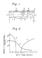
- an n+ type buried layer 2 is formed on a p type semiconductor substrate 1, and an n type semiconductor layer 3 acting as a collector is formed thereon.
- boron ions are implanted only into a base formation region using a resist mask (not shown) having an opening thereat, to form a base 5, and subsequently, for example, arsenic ions, are implanted into an emitter formation region using a resist mask having an opening thereat to form an emitter 6.
- Fig. 1, 8 is a field insulating film and C, B and E are a collector electrode, a base electrode, and an emitter electrode, respectively.
- the electric properties of the semiconductor device are represented as follows.
- ⁇ is a base transportation efficiency
- W B base layer thickness
- L nB base diffusion length
- h FE emitter earth current amplification ratio
- ⁇ emitter implanting efficiency
- f ⁇ cut off frequency.
- the equation (a) shows that, when the base layer thickness W B is narrowed, the base transportation efficiency ⁇ becomes large
- the equation (b) shows that, when the base transportation ⁇ becomes large, the emitter earth current amplification ratio h FE becomes large.
- the equation (c) shows that, when the base layer thickness W B is narrowed, the cut off frequency f ⁇ , which represents an operating frequency limit of a transistor, becomes high.
- a decrease of the ion implanting acceleration energy for impurity ions has been considered as a method of narrowing the base layer thickness W B , but in this case, channeling occurs, and as shown in Fig. 2 by a curve p, the base layer thickness is diffused into the inner portion of a semiconductor substrate. Therefore, to form a base layer having a thickness of 2000 to 3000 ⁇ or less is difficult in practice.
- the curves Q and R show the impurity concentration distribution in an emitter region and a collector region, respectively.
- 11 is an n type silicon layer such as an n type silicon substrate or n type silicon epitaxial layer, etc., 12 an SiO2 layer acting as an isolation region, 13 a gate insulating film having a thickness of 200 ⁇ , e.g., an SiO2 layer, 14 a gate electrode of polycrystalline silicon layer, 16 and 17 p+ source and drain regions, and 18 and 19 p ⁇ regions having an LDD.
- n type silicon layer such as an n type silicon substrate or n type silicon epitaxial layer, etc.
- 12 an SiO2 layer acting as an isolation region
- 13 a gate insulating film having a thickness of 200 ⁇ , e.g., an SiO2 layer
- 14 a gate electrode of polycrystalline silicon layer
- 16 and 17 p+ source and drain regions and 18 and 19 p ⁇ regions having an LDD.
- the voltage used in a semiconductor device is generally constant, regardless of the size of the element, the carrier speed is increased near a drain region in a short channel FET, and a hot carrier effect is generated, and thus the insulation between a gate electrode and a drain might be broken.
- This phenomenon is particularly remarkable in an n channel type FET having electron carriers, but the same phenomenon can be recognized even in a p channel type FET.
- LDD low impurity concentration region
- the LDD region preferably has a thin thickness of 1000 ⁇ or less, when boron arsenic, and phosphorus, etc., are ion-implanted to form the LDD region, an LDD region having a thickness of 2500 ⁇ or less can not be easily formed due to the channelling, etc.
- the LDD region can be also formed by forming a boron oxide film using a thermal CVD process or plasma CVD process except fcr an ion implanting process and carrying out a heat treatment.
- An object of the present invention is to provide a method of forming a shallow junction by forming a impurity diffusion layer having a thickness of 1000 ⁇ or less and an impurity concentration of 1018 to 1021 cm ⁇ 3 without damaging the silicon layer.
- a further object of the present invention is to provide a semiconductor device having a shallow junction, such as a bipolar transistor and MOS transistor, in which a channeling effect is prevented.
- a method of forming a shallow junction comprising the steps of: forming a film including a hydrogen compound with one element selected from the group of boron, phosphorus and arsenic with to a thickness from several atom layers to 1000 ⁇ on a silicon substrate and annealing the film, whereby an impurity region having a depth of 1000 ⁇ or less and having an impurity concentration of 1018 to 1021 in the surface layer of the silicon layer is obtained.
- the thickness of the film including the hydrogen compound with one element selected from the group of boron (B), phosphorus (P) and arsenic (As) is preferably from several atom layers to 200 ⁇ to obtain a shallower junction.
- the annealing is preferably carried out by furnace annealing at 800 to 950°C and by a lamp annealing at 1000 to 1150°C.
- a method of producing an npn type bipolar transistor having a shallow junction comprising the steps of, forming a film including a hydrogen compound with one element selected frcm the group of boron phosphorus and arsenic on a first conductivity type silicon layer acting as a collector, annealing the film and the silicon layer to diffuse the one element included in the film into the n type silicon so that a base having a thickness of 1000 ⁇ or less is formed, and forming an emitter of a silicon layer containing said first conductivity type impurities on a part of the base.
- a method of producing a MOS transistor having a shallow source and drain comprising the steps of: forming a gate insulating layer and a gate electrode on a first conductivity type silicon layer, forming a film including a hydrogen compound with one element selected from the group of boron, phosphorus and arsenic on said first conductive type silicon layer, annealing the film and said first conductivity type silicon layer to diffuse the one element selected from the group of boron, phosphorus and arsenic into said silicon layer, whereby a second conductivity type silicon layer having a thickness of 1000 ⁇ or less and an impurity concentration of 1018 to 1021 cm ⁇ 3 is formed in said first conductivity type silicon layer, forming a drain formation mask at the side wall of the gate electrode, and introducing a second conductivity type impurity into the first conductivity type silicon layer using both the gate electrode and the side wall thereof as a mask.
- a bipolar transistor comprising a shallow base silicon layer having a thickness of 1000 ⁇ or less and having an impurity concentration of 1018 to 1021 cm ⁇ 3, and a MOS transistor comprising a shallow source and drain silicon layer having a thickness of 1000 ⁇ or less and having an impurity concentration of 1018 to 1021 cm ⁇ 3.
- a method of forming a silicon layer having a thickness of 1000 ⁇ or less and an impurity concentration of 1018 to 1021 cm ⁇ 3 will be explained.
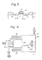
- FIG. 4 shows a schematic cross-sectional view of a non-bias dispersion magnetic field type Electron Cyclotron Resonance (ECR) plasma CVD apparatus used for forming a thin film of impurity atoms of boron, phosphorus or arsenic according to the present invention.
- ECR Electron Cyclotron Resonance
- 21 is a wave guide by which an exciting microwave of, for example, 2.45 GHz, is guided.
- the exciting microwave is introduced into a plasma generating chamber 24 through a microwave introducing window 21a, 23 is a magnetic field generating meanings for generating plasma which usually provides about 875 gauss.
- a reactive gas supplied through a gas supply opening 24a is plasmanized by the exciting microwave.
- the plasma is confined in the plasma generating chamber 24.
- Reference 26 is a reaction chamber (thin film forming chamber) having a plasma feed opening 22 in which a supporting means 25, which supports a silicon substrate 20, is provided.
- the temperature of the supporting means 25 is controlled by a cooling means 25a.
- the reaction gas related to the reaction is discharged through an exhaust system 27a. No bias voltage is applied against the substrate 20.
- the feature of the non-bias dispersion magnetic field type ECR plasma CVD apparatus is that, as shown in Fig. 5, the plasma potential intensity is sharply reduced from the left side of the plasma generating chamber 24 to the right side of the reaction chamber 26.
- the plasma potential of the reactive gas is reduced from 10 to 25 V near the supporting means 25.
- a mixed gas of B2H6 and an inactive gas such as Ar, He, H2 is used as the reacting gas.
- an n type silicon layer is formed by diffusing n type impurities, a mixed gas of pH3 and inactive gas, for example, Ar, He, H2 or AsH3 , is used as a reacting gas.
- the concentration of an active layer can be controlled by controlling the source gas concentration, film growth time, and annealing temperature, etc.
- the above-mentioned reacting gas is supplied so that the internal pressure of the reaction chamber 26 becomes 0.1 to 0.2 Pa.
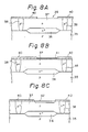
- boron, phosphorus or arsenic, etc. is deposited on the silicon substrate 20. Since the energy having atoms of boron phosphorus or arsenic, etc., is 10 to 20 V, which is extremely low, the temperature of the silicon substrate 20 is 150°C or less. Therefore, boron, phosphorus or arsenic is deposited on the silicon substrate 20 without damage as an extremely thin film having thickness of the atom layer order as shown in Fig. 6A.
- vacuum annealing is carried out at a temperature of 900°C or less under a vacuum, and the boron, phosphorus or arsenic of the boron, phosphorus or arsenic thin film is diffused to a region having a thickness of 1000 ⁇ or less, whereby a p (or n) type silicon layer having a thickness of 1000 ⁇ or less and containing an impurity concentration of 1018 to 1021 cm ⁇ 3 is formed as shown in Fig. 6B.
- LDD FET Lightly Doped Drain Field Effect Transistor
- a thick SiO2 layer 12 is formed at an isolation region of a surface of an n type silicon layer 11 using a LOCOS process. Then, using a CVD process, an SiO2 layer 13a having a thickness of 100 to 200 ⁇ is formed on the silicon layer 11. Subsequently, a polycrystalline silicon layer 14a having a thickness of 5000 ⁇ is formed.
- the stack of the SiO2 layer 13a and the polycrystalline silicon layer 14a is patterned so that a gate insulating film 13 and a gate electrode 14 are formed.
- a boron layer 30 having a thickness of 1000 ⁇ or less is formed by an ECR plasma CVD process using a reacting gas of B2H6 and an inactive gas, for example, Ar, He, and H2 as explained in Example 1.
- the microwave wavelength used for forming the boron layer 30 is, for example, 2.45 GHz, and the magnetic field intensity is 875 gauss, the device internal pressure is 0.1 to 0.2 Pa and the deposition time is about 20 secs when the microwave power is 200 to 1 kW.
- boron phosphorus or arsenic of the boron, phosphorus or arsenic thin film 30 is diffused to a region having a thickness of 1000 ⁇ or less, and a p type (or n type) region 31 having a p type (or n type) impurity concentration of 1019 cm ⁇ 3 is formed.
- an SiO2 layer 32 having a thickness of about 3000 ⁇ is formed by using a well known CVD process.
- the SiO2 layer 32 is etched by a reactive ion etching (RIE) process so that an SiO2 layer 33 remains at the side wall of the gate electrode 14.
- RIE reactive ion etching
- BF2 or B is ion implanted at an implanting pressure of about 40 keV and a dosage of about 3 x 1015 cm ⁇ 2, and subsequently, annealing is carried out at a temperature of 900°C in a nitrogen atmosphere so that a p+ source 16 and p+ drain 17 are formed.
- annealing is carried out at a temperature of 900°C in a nitrogen atmosphere so that a p+ source 16 and p+ drain 17 are formed.
- the p type region 30 covered by the SiO2 layer 33 becomes the LDD's 18 and 19.
- an field effective transistor provided with LDD's 18 and 19 having an impurity concentration of about 1019 cm ⁇ 3 and a thickness of 1000 ⁇ or less is obtained.
- the LDD's 18 and 19 act as a shallow junction.
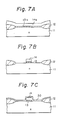
- an n+ type buried layer 36 is formed on a p type silicon substrate 35 and an n type silicon single crystalline layer 37 is formed thereof. After introducing p type impurities to an isolation region a p+ type silicon isolation layer 38 is formed.
- a base formation mask 40 having an opening 39 is formed at a base formation region mask 40.
- the obtained silicon substrate 35 is then set on the support means 25 as shown in Fig. 4.
- the pressure in the plasma generating chamber 24 and the reaction chamber 26 is maintained at 6 x 10 ⁇ 3 Torr or less, and the cooling means 25a is controlled so that a temperature of 20 to 150°C is maintained. Further, a bias voltage is not applied to the silicon substrate 35.
- Argon gas containing 1 to 5% of diborane (B2H6) is fed into the plasma generating chamber having a volume of 8.5 x 8.5 x ⁇ x 19 cm3 or 5.7l, at a supply rate of about 30 cc/min, and a microwave having a power of 200 to 800 W and a frequency of 2.45 GHz is introduced to the plasma generating chamber 24 through the microwave introduction window 21a.
- B2H6 diborane
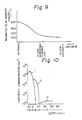
- a dispersion type magnetic field formed by the dispersion type formation means 23 is generated as shown in Fig. 9.
- the magnetic flux density is about 875 gauss at the entrance side of the plasma generating chamber 24, and is about 300 gauss near the plasma feed opening 22. Therefore, as shown in Fig. 9, the magnetic flux density is gradually reduced. Consequently, B2H6 supplied from the gas supply opening 24a is excited and the excited boron, i.e., boron atoms, boron radicals or boron ions, is moved tc the reaction chamber 26 together with plasma generated in the plasma generating chamber 24.
- the excited boron i.e., boron atoms, boron radicals or boron ions
- the excited boron After the translation of the excited boron is completed, it collides with the silicon substrate 35 at a low speed, which is accelerated by a low accelerated energy, e.g., about 20 V, so that a boron thin film 41 having a thickness of several hundreds is formed on a base formation region of the silicon substrate as shown in Fig. 8B.
- the time required to form the boron film is from several seconds to several minutes.
- the boron thin film 41 is non-metallic and atomic.
- the obtained silicon substrate 35 is annealed at a temperature of 800 to 900°C for about 30 minutes under a nitrogen or hydrogen gas atmosphere and a reduced pressure of 1 to 4 Torr, whereby an improved thin p type base 42 is formed in the n type silicon layer 37 acting as a collector without losing the crystallizability thereof as shown in Fig. 8C.
- the thickness of the base 42 is 1000 ⁇ or less.
- an SiO2 film is formed on a base 42 and a part of the SiO2 , corresponding to an emitter formation region is removed so that a emitter formation mask 43 is formed.
- a polycrystalline silicon film is formed on only the emitter region 44, n type impurities are implanted into the polycrystalline silicon film to form an emitter 44.
- a SiO2 film is fo9rmed on the emitter 44, and electrode contact windows are formed in the collector electrcde formation region, the base electrode formation region, and the emitter electrode formation region, and after forming an aluminum film over the entire surface, patterned so that a collector electrode C, a base electrode B and an emitter electrode E are formed, whereby a shallow base type bipolar transistor can be realized.
- the bipolar structure has a shallow junction.
- Figure 10 shows an impurity concentration profile of a shallow base type bipolar transistor produced by above-explained processes.
- the curve S is an impurity concentration profile of a base.
- the base width (thickness) is 40 nm and the impurity concentration of the base is 3 x 1019 cm ⁇ 3.
- the curve T is an impurity concentration profile of an emitter layer formed on the base, and the curve U is an impurity concentration profile of a collector.
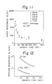
- Figure 11 is a graph showing a relationship between a sheet resistance ⁇ S ( ⁇ / ⁇ ) in which a microwave power is changed from 200 W to 1 kW and a growth time (sec). In the growth process, a heat treatment was carried out at 900°C for 30 minutes under an N2 atmosphere at a reduced pressure. This graph shown that the sheet resistance does not depend on the microwave power.
- Figure 12 shows a relationship between the surface resistance ⁇ S ( ⁇ / ) and the growth time in the absence or presence of oxygen in a plasma generating chamber the curve I is the case in the absence of oxygen and the curve II is the case in the presence of oxygen.
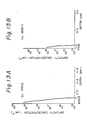
- Figures 13A and 13B show the impurity concentration (cm ⁇ 3) in a depth direction obtained by a measurement by a secondary ion mass spectroscopy (SIMS).
- the growth conditions are as follows: microwave power: 200 W, growth time: 20 sec, gas supply rate: 30 cc of Ar gas in which the 1% of B2H6 is contained per minutes, heat treatment (annealing): at a temperature of 850°C, for 30 min in an N2 atmosphere under a reduced pressure.
- Fig. 13A shows a growth method in an oxygen free atmosphere.
- a p type impurity diffusion layer having a surface concentration of 2 x 1019 cm ⁇ 3 and a thickness of about 1000 ⁇ is formed.
- Fig. 13B shows a growth method in an oxygen containing atmosphere, wherein the surface impurity concentration becomes 1 x 1018 cm ⁇ 3 and the depth of the impurity region becomes about 340 ⁇ , whereby the surface impurity concentration and the depth of the impurity diffusion layer are remarkably reduced. Further, as shown by the measurement by a SIMS, channeling is not generated.
Landscapes
- Bipolar Transistors (AREA)
- Insulated Gate Type Field-Effect Transistor (AREA)
Applications Claiming Priority (6)
| Application Number | Priority Date | Filing Date | Title |
|---|---|---|---|
| JP33572087 | 1987-12-30 | ||
| JP335720/87 | 1987-12-30 | ||
| JP104018/88 | 1988-04-28 | ||
| JP10401888 | 1988-04-28 | ||
| JP171359/88 | 1988-07-08 | ||
| JP17135988 | 1988-07-08 |
Publications (2)
| Publication Number | Publication Date |
|---|---|
| EP0322921A2 true EP0322921A2 (de) | 1989-07-05 |
| EP0322921A3 EP0322921A3 (de) | 1990-08-16 |
Family
ID=27310128
Family Applications (1)
| Application Number | Title | Priority Date | Filing Date |
|---|---|---|---|
| EP88121891A Ceased EP0322921A3 (de) | 1987-12-30 | 1988-12-30 | Verfahren zur Bildung von flachen Übergängen und Halbleiterbauelement mit flachen Übergängen |
Country Status (2)
| Country | Link |
|---|---|
| EP (1) | EP0322921A3 (de) |
| KR (1) | KR910009030B1 (de) |
Cited By (11)
| Publication number | Priority date | Publication date | Assignee | Title |
|---|---|---|---|---|
| EP0413982A1 (de) * | 1989-07-27 | 1991-02-27 | Junichi Nishizawa | Dotierungsverfahren mittels einer adsorbierten Diffusionquelle |
| EP0417456A3 (en) * | 1989-08-11 | 1991-07-03 | Seiko Instruments Inc. | Method of producing semiconductor device |
| EP0431444A3 (en) * | 1989-12-06 | 1992-03-18 | Seiko Instruments Inc. | Method of producing mis transistor having gate electrode of matched conductivity type |
| EP0430274A3 (en) * | 1989-12-01 | 1993-03-24 | Seiko Instruments Inc. | Method of producing bipolar transistor |
| EP0430167A3 (en) * | 1989-12-01 | 1993-08-11 | Seiko Instruments Inc. | Method or producing pn junction device |
| US5284793A (en) * | 1989-11-10 | 1994-02-08 | Kabushiki Kaisha Toshiba | Method of manufacturing radiation resistant semiconductor device |
| EP0606114A1 (de) * | 1989-08-11 | 1994-07-13 | Seiko Instruments Inc. | Verfahren zur Herstellung eines Feldeffekttransistors |
| US5338697A (en) * | 1989-12-01 | 1994-08-16 | Seiko Instruments Inc. | Doping method of barrier region in semiconductor device |
| US5366922A (en) * | 1989-12-06 | 1994-11-22 | Seiko Instruments Inc. | Method for producing CMOS transistor |
| US5532185A (en) * | 1991-03-27 | 1996-07-02 | Seiko Instruments Inc. | Impurity doping method with adsorbed diffusion source |
| EP0663689A3 (de) * | 1993-12-27 | 1998-01-28 | AT&T Corp. | Diffundierungsverfahren für integrierte Schaltkreise |
Families Citing this family (1)
| Publication number | Priority date | Publication date | Assignee | Title |
|---|---|---|---|---|
| KR101610895B1 (ko) | 2015-06-30 | 2016-04-08 | 성균관대학교산학협력단 | 원자층 접합 산화물 및 이의 제조 방법 |
Family Cites Families (3)
| Publication number | Priority date | Publication date | Assignee | Title |
|---|---|---|---|---|
| US4382099A (en) * | 1981-10-26 | 1983-05-03 | Motorola, Inc. | Dopant predeposition from high pressure plasma source |
| US4621411A (en) * | 1984-09-28 | 1986-11-11 | Texas Instruments Incorporated | Laser-enhanced drive in of source and drain diffusions |
| US4619036A (en) * | 1984-09-28 | 1986-10-28 | Texas Instruments Incorporated | Self-aligned low-temperature emitter drive-in |
-
1988
- 1988-12-28 KR KR1019880017673A patent/KR910009030B1/ko not_active Expired
- 1988-12-30 EP EP88121891A patent/EP0322921A3/de not_active Ceased
Cited By (16)
| Publication number | Priority date | Publication date | Assignee | Title |
|---|---|---|---|---|
| EP0413982A1 (de) * | 1989-07-27 | 1991-02-27 | Junichi Nishizawa | Dotierungsverfahren mittels einer adsorbierten Diffusionquelle |
| US5527733A (en) * | 1989-07-27 | 1996-06-18 | Seiko Instruments Inc. | Impurity doping method with adsorbed diffusion source |
| US5851909A (en) * | 1989-08-11 | 1998-12-22 | Seiko Instruments Inc. | Method of producing semiconductor device using an adsorption layer |
| EP0417456A3 (en) * | 1989-08-11 | 1991-07-03 | Seiko Instruments Inc. | Method of producing semiconductor device |
| EP0606114A1 (de) * | 1989-08-11 | 1994-07-13 | Seiko Instruments Inc. | Verfahren zur Herstellung eines Feldeffekttransistors |
| US5284793A (en) * | 1989-11-10 | 1994-02-08 | Kabushiki Kaisha Toshiba | Method of manufacturing radiation resistant semiconductor device |
| US5925574A (en) * | 1989-12-01 | 1999-07-20 | Seiko Instruments Inc. | Method of producing a bipolar transistor |
| EP0430274A3 (en) * | 1989-12-01 | 1993-03-24 | Seiko Instruments Inc. | Method of producing bipolar transistor |
| EP0430167A3 (en) * | 1989-12-01 | 1993-08-11 | Seiko Instruments Inc. | Method or producing pn junction device |
| US5338697A (en) * | 1989-12-01 | 1994-08-16 | Seiko Instruments Inc. | Doping method of barrier region in semiconductor device |
| US5514620A (en) * | 1989-12-01 | 1996-05-07 | Seiko Instruments Inc. | Method of producing PN junction device |
| US5366922A (en) * | 1989-12-06 | 1994-11-22 | Seiko Instruments Inc. | Method for producing CMOS transistor |
| US5874352A (en) * | 1989-12-06 | 1999-02-23 | Sieko Instruments Inc. | Method of producing MIS transistors having a gate electrode of matched conductivity type |
| EP0431444A3 (en) * | 1989-12-06 | 1992-03-18 | Seiko Instruments Inc. | Method of producing mis transistor having gate electrode of matched conductivity type |
| US5532185A (en) * | 1991-03-27 | 1996-07-02 | Seiko Instruments Inc. | Impurity doping method with adsorbed diffusion source |
| EP0663689A3 (de) * | 1993-12-27 | 1998-01-28 | AT&T Corp. | Diffundierungsverfahren für integrierte Schaltkreise |
Also Published As
| Publication number | Publication date |
|---|---|
| EP0322921A3 (de) | 1990-08-16 |
| KR910009030B1 (ko) | 1991-10-28 |
| KR890011102A (ko) | 1989-08-12 |
Similar Documents
| Publication | Publication Date | Title |
|---|---|---|
| US5183777A (en) | Method of forming shallow junctions | |
| US5767557A (en) | PMOSFETS having indium or gallium doped buried channels and n+polysilicon gates and CMOS devices fabricated therefrom | |
| EP0137645B1 (de) | Verfahren zur Bildung eines seichten Gebietes des N-Typs | |
| EP0139467B1 (de) | Verfahren zum Herstellen eines Feldeffekttransistors mit isoliertem Gate | |
| KR100294089B1 (ko) | Mis형반도체장치제작방법 | |
| US4810665A (en) | Semiconductor device and method of fabrication | |
| US4437897A (en) | Fabrication process for a shallow emitter/base transistor using same polycrystalline layer | |
| EP0322161A2 (de) | Siliciumcarbidsperre zwischen einem Siliciumsubstrat und einer Metallschicht | |
| EP0322921A2 (de) | Verfahren zur Bildung von flachen Übergängen und Halbleiterbauelement mit flachen Übergängen | |
| EP0076106B1 (de) | Verfahren zur Herstellung eines bipolaren Transistors | |
| US6171917B1 (en) | Transistor sidewall spacers composed of silicon nitride CVD deposited from a high density plasma source | |
| US20100015788A1 (en) | Method for manufacturing semiconductor device | |
| US5238849A (en) | Method of fabricating semiconductor device | |
| US5747371A (en) | Method of manufacturing vertical MOSFET | |
| CN117238914B (zh) | 一种集成SBD的SiC器件及制备方法 | |
| JPS5947468B2 (ja) | バイポ−ラ・トランジスタの製造方法 | |
| CN117219660A (zh) | 一种基于栅极掩埋的mosfet器件及制备方法 | |
| EP0589631B1 (de) | Verfahren für vertiefte, selbstausgerichtete Basisstruktur mit niedrigem Widerstand | |
| JP2917348B2 (ja) | Mis型半導体装置の製造方法 | |
| Juang et al. | Formation of shallow p+ n junctions by implanting BF2− ions into thin cobalt films on silicon substrates | |
| EP0042380B1 (de) | Verfahren zum erreichen eines idealen fremdstoffkonzentrationsverlaufs für die basiszone eines transistors | |
| JP3578345B2 (ja) | 半導体装置の製造方法および半導体装置 | |
| EP0262034B1 (de) | Dotierungsmethode mittels Verunreinigungen für die Herstellung von Halbleiterbauelementen | |
| JPH02132823A (ja) | 浅い接合を形成する方法及びその浅い接合を有する半導体装置 | |
| JPH0595000A (ja) | 半導体装置の製造方法 |
Legal Events
| Date | Code | Title | Description |
|---|---|---|---|
| PUAI | Public reference made under article 153(3) epc to a published international application that has entered the european phase |
Free format text: ORIGINAL CODE: 0009012 |
|
| AK | Designated contracting states |
Kind code of ref document: A2 Designated state(s): DE FR GB |
|
| PUAL | Search report despatched |
Free format text: ORIGINAL CODE: 0009013 |
|
| AK | Designated contracting states |
Kind code of ref document: A3 Designated state(s): DE FR GB |
|
| 17P | Request for examination filed |
Effective date: 19901219 |
|
| 17Q | First examination report despatched |
Effective date: 19930129 |
|
| STAA | Information on the status of an ep patent application or granted ep patent |
Free format text: STATUS: THE APPLICATION HAS BEEN REFUSED |
|
| 18R | Application refused |
Effective date: 19950130 |