EP0323073A2 - Wavelength conversion using self electrooptic effect devices - Google Patents
Wavelength conversion using self electrooptic effect devices Download PDFInfo
- Publication number
- EP0323073A2 EP0323073A2 EP88311779A EP88311779A EP0323073A2 EP 0323073 A2 EP0323073 A2 EP 0323073A2 EP 88311779 A EP88311779 A EP 88311779A EP 88311779 A EP88311779 A EP 88311779A EP 0323073 A2 EP0323073 A2 EP 0323073A2
- Authority
- EP
- European Patent Office
- Prior art keywords
- quantum well
- wavelength
- diode
- well region
- semiconductor material
- Prior art date
- Legal status (The legal status is an assumption and is not a legal conclusion. Google has not performed a legal analysis and makes no representation as to the accuracy of the status listed.)
- Granted
Links
Images
Classifications
-
- G—PHYSICS
- G02—OPTICS
- G02F—OPTICAL DEVICES OR ARRANGEMENTS FOR THE CONTROL OF LIGHT BY MODIFICATION OF THE OPTICAL PROPERTIES OF THE MEDIA OF THE ELEMENTS INVOLVED THEREIN; NON-LINEAR OPTICS; FREQUENCY-CHANGING OF LIGHT; OPTICAL LOGIC ELEMENTS; OPTICAL ANALOGUE/DIGITAL CONVERTERS
- G02F1/00—Devices or arrangements for the control of the intensity, colour, phase, polarisation or direction of light arriving from an independent light source, e.g. switching, gating or modulating; Non-linear optics
- G02F1/01—Devices or arrangements for the control of the intensity, colour, phase, polarisation or direction of light arriving from an independent light source, e.g. switching, gating or modulating; Non-linear optics for the control of the intensity, phase, polarisation or colour
- G02F1/015—Devices or arrangements for the control of the intensity, colour, phase, polarisation or direction of light arriving from an independent light source, e.g. switching, gating or modulating; Non-linear optics for the control of the intensity, phase, polarisation or colour based on semiconductor elements having potential barriers, e.g. having a PN or PIN junction
- G02F1/017—Structures with periodic or quasi periodic potential variation, e.g. superlattices, quantum wells
- G02F1/01716—Optically controlled superlattice or quantum well devices
-
- B—PERFORMING OPERATIONS; TRANSPORTING
- B82—NANOTECHNOLOGY
- B82Y—SPECIFIC USES OR APPLICATIONS OF NANOSTRUCTURES; MEASUREMENT OR ANALYSIS OF NANOSTRUCTURES; MANUFACTURE OR TREATMENT OF NANOSTRUCTURES
- B82Y20/00—Nanooptics, e.g. quantum optics or photonic crystals
-
- G—PHYSICS
- G02—OPTICS
- G02F—OPTICAL DEVICES OR ARRANGEMENTS FOR THE CONTROL OF LIGHT BY MODIFICATION OF THE OPTICAL PROPERTIES OF THE MEDIA OF THE ELEMENTS INVOLVED THEREIN; NON-LINEAR OPTICS; FREQUENCY-CHANGING OF LIGHT; OPTICAL LOGIC ELEMENTS; OPTICAL ANALOGUE/DIGITAL CONVERTERS
- G02F2/00—Demodulating light; Transferring the modulation of modulated light; Frequency-changing of light
- G02F2/004—Transferring the modulation of modulated light, i.e. transferring the information from one optical carrier of a first wavelength to a second optical carrier of a second wavelength, e.g. all-optical wavelength converter
-
- G—PHYSICS
- G02—OPTICS
- G02F—OPTICAL DEVICES OR ARRANGEMENTS FOR THE CONTROL OF LIGHT BY MODIFICATION OF THE OPTICAL PROPERTIES OF THE MEDIA OF THE ELEMENTS INVOLVED THEREIN; NON-LINEAR OPTICS; FREQUENCY-CHANGING OF LIGHT; OPTICAL LOGIC ELEMENTS; OPTICAL ANALOGUE/DIGITAL CONVERTERS
- G02F3/00—Optical logic elements; Optical bistable devices
- G02F3/02—Optical bistable devices
- G02F3/028—Optical bistable devices based on self electro-optic effect devices [SEED]
Definitions
- This invention relates to the field of optical devices and, more particularly, to devices comprising semiconductor quantum wells utilizing the self electrooptic effect.
- Quantum well devices have been developed recently to provide classical optical communication system functions such as modulation, detection, and optical signal generation. See, for example, U. S. Patent 4,525,687. By employing the nonlinear bistability of certain devices, it has been possible to extend the growth of quantum well devices into the areas of switching systems and optical computing. In the latter areas, quantum well devices have been fabricated as basic Boolean logic devices such as AND and OR gates, complex memory and processing devices such as S-R flip-flops and logic device arrays for parallel processing, and switching devices such as n x n switching arrays.
- Boolean logic devices such as AND and OR gates
- complex memory and processing devices such as S-R flip-flops and logic device arrays for parallel processing
- switching devices such as n x n switching arrays.
- a photocurrent generated from the absorption of optical energy by a diode may change the voltage across the diode which, in turn, causes a change in the absorption characteristic of the diode.
- the diode is generally a GaAs/AlGaAs p-i-n structure wherein the intrinsic region (i) comprises one or more quantum well layers. Connection of the diode to a proper electrical load such as a resistive load and tuning the optical signal wavelength coincidently with the heavy hole exciton resonance wavelength permits switching and bistable behavior (hysteretic operation) to be achieved via a positive feedback mechanism.
- a symmetric SEED device in which two serially connected p-i-n photodiodes are fabricated with substantially identical quantum well layers in the respective intrinsic regions. See Conference on Lasers and Electrooptics , Paper ThT12 (1987). This structure is called symmetric because each photodiode operates as the load for the other. It has been proposed that this structure act as a bistable optical memory element such as an optical S-R flip-flop. As an S-R flip-flop, the structure supports dual inputs and dual outputs wherein the optical wavelengths for all inputs and outputs are identical.
- a device as set out in the claims is capable of receiving dual input optical signals at different wavelengths and, in response to the dual input signals, generating dual output signals at the corresponding different wavelengths wherein at least one output signal is functionally related to the input signal of the different wavelength. For example, it is possible for information borne by an optical signal at a first wavelength to be transferred intact to another optical signal at a second wavelength and vice versa.
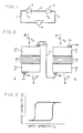
- FIG. 1 shows a schematic diagram of two reverse-biased multiple quantum well diodes arranged electrically in series in accordance with the principles of this invention.
- Diode 2 includes a quantum well region responsive to optical signals substantially at wavelength ⁇ 1.
- Diode 4 includes a quantum well region responsive to optical signals substantially at wavelength ⁇ 2.
- Diodes 2 and 4 are connected in series aiding configuration via electrical lead 3. Reverse bias voltage is applied to the diodes by source 6 connected to diode 2 via electrical lead 1 and connected to diode 4 via electrical lead 5.
- the optoelectronic circuit shown in FIG. 1 was realized as a hybrid circuit using discrete components.
- FIG. 2 shows a simplified cross-sectional layer diagram for the exemplary devices included in the optoelectronic circuit of FIG. 1. It will be understood by those skilled in the art that the layers shown in the FIG. are not drawn to scale and only depict the important active layers while others such as the substrate have been omitted.
- diode 2 comprises a p-i-n quantum well photodiode structure in which layer 21 is n-doped InP (1.0 ⁇ m thickness), intrinsic region 22 includes a plurality of alternating layers ( ⁇ 100 pairs) of InGaAs wells (10 nm thickness) and InP barriers (10 nm thickness) to form the quantum well region, and layer 23 in p-doped InP (1.0 ⁇ m thickness).
- diode 4 comprises a p-i-n quantum well photodiode structure in which layer 41 is n-doped AlGaAs(1.0 ⁇ m thickness), intrinsic region 42 includes a plurality of alternating layers ( ⁇ 100 pairs) of GaAs wells (10 nm thickness) and AlGaAs barriers (10 nm thickness) to form the quantum well region, and layer 43 in p-doped AlGaAs (1.0 ⁇ m thickness). Electrical contact is made to layer 41 via metallic contact 45 and to layer 43 via metallic contact 45. Biasing potential of 20 volts is supplied to contact 24 (V-) and contact 44(V+) to achieve a reverse bias condition.
- the diodes are interconnected in series-aiding configuration via lead 3 connecting contacts 25 and 44.
- light beams 30 and 31 are directed on diodes 2 and 4, respectively.
- light beam 33 emerges from diode 4 bearing the modulation information from light beam 30 but at the wavelength ⁇ 2.
- light beam 32 emerges from diode 2 bearing the modulation information from light beam 31 but at the wavelength ⁇ 1.
- GaAs/AlGaAs/InP quantum well devices has been described above, it is to be understood by those skilled in the art that other combinations of Quantum well types are possible.
- combinations of quantum wells from the Group III-V system of semiconductor compounds such as InGaAsP/InP, GaAs/AlGaAs, GaSb/GaAlSb and InGaAs/InP and the like may be substituted for the quantum well regions shown in FIG. 2 to achieve modulation conversation at other wavelengths.
- FIG. 3 shows an actual graphical plot of the output intensity for the optical signal from diode 4 at wavelength ⁇ 2 as a function of the input intensity of the optical signal from diode 2 at wavelength ⁇ 1.
- the experimental configuration and procedures which produced these results have been described above in reference to FIG. 1.
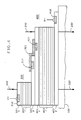
- FIG. 4 shows a cross-sectional view of an integrated semiconductor circuit embodying the principles of the present invention.
- the integrated circuit comprises two series-aiding multiple quantum well photodiodes grown on InP substrate 100.
- Substrate 100 is transparent to the operating wavelengths of interest thereby permitting optical access to the active regions of the device.
- Diodes 200 and 400 comprise epitaxial p-type, intrinsic and n-type layers. Doping concentrations are generally in the range 1017 to 1018cm ⁇ 3.
- n-doped layer 201 is approximately 1 ⁇ m thick InGaAsP; intrinsic region 202 comprises approximately 100 pairs of thin (10nm) InGaAs well layers and InGaAsP barrier layers; and p-doped layer 203 is approximately 1 ⁇ m thick InGaAsP. Both the InGaAsP ( ⁇ 1.3 ⁇ m) and the InGaAs (( ⁇ 1.5 ⁇ m) are selected to be lattice matched to InP. Alloyed contact 210 is formed in n-doped layer 201 for connection to the power supply. Alloyed contact 211 is formed in p-doped layer 203 for interconnection from diode 200 to diode 400 via gold interconnection pad 301. Diode 200 is responsive to input light beam 300 at a wavelength of 1.5 ⁇ m. Light beam 320 at 1.5 ⁇ m is the output beam for diode 200.
- n-doped layer 401 is approximately 1 ⁇ m thick InP; intrinsic region 402 comprises approximately 100 pairs of thin (10 nm) InGaAsP well layers and InP barrier layers; and p-doped layer 403 is approximately 1 ⁇ m thick InP. InGaAsP ( ⁇ 1.3 ⁇ m) is selected to be lattice matched to InP. Alloyed contact 410 is formed in p-doped layer 403 for connection to the power supply. Alloyed contact 411 is formed in n-doped layer 401 for interconnection from diode 400 to diode 200 via gold interconnection pad 301. Diode 400 is responsive to input light beam 310 at a wavelength of 1.3 ⁇ m. Light beam 330 at 1.3 ⁇ m is the output beam, for diode 400.
- the optoelectronic circuit may be utilized in a waveguide mode with a possible reduction of the number of layers in the intrinsic region and a possible elimination of the biasing source. It is also understood that in such a waveguide structure proper fabrication of the layer thicknesses may result in an antiresonant reflector optical waveguide with vertical coupling between the photodiodes.
Landscapes
- Physics & Mathematics (AREA)
- Nonlinear Science (AREA)
- Optics & Photonics (AREA)
- General Physics & Mathematics (AREA)
- Chemical & Material Sciences (AREA)
- Engineering & Computer Science (AREA)
- Nanotechnology (AREA)
- Life Sciences & Earth Sciences (AREA)
- Biophysics (AREA)
- Crystallography & Structural Chemistry (AREA)
- Light Receiving Elements (AREA)
- Photo Coupler, Interrupter, Optical-To-Optical Conversion Devices (AREA)
Abstract
Description
- This invention relates to the field of optical devices and, more particularly, to devices comprising semiconductor quantum wells utilizing the self electrooptic effect.
- Quantum well devices have been developed recently to provide classical optical communication system functions such as modulation, detection, and optical signal generation. See, for example, U. S. Patent 4,525,687. By employing the nonlinear bistability of certain devices, it has been possible to extend the growth of quantum well devices into the areas of switching systems and optical computing. In the latter areas, quantum well devices have been fabricated as basic Boolean logic devices such as AND and OR gates, complex memory and processing devices such as S-R flip-flops and logic device arrays for parallel processing, and switching devices such as n x n switching arrays.
- Improvements to the latter quantum well devices have centered on the development of the self electrooptic effect device, more commonly referenced as the SEED device. See U. S. Patent 4,546,244. In the operation of the SEED device, a photocurrent generated from the absorption of optical energy by a diode may change the voltage across the diode which, in turn, causes a change in the absorption characteristic of the diode. The diode is generally a GaAs/AlGaAs p-i-n structure wherein the intrinsic region (i) comprises one or more quantum well layers. Connection of the diode to a proper electrical load such as a resistive load and tuning the optical signal wavelength coincidently with the heavy hole exciton resonance wavelength permits switching and bistable behavior (hysteretic operation) to be achieved via a positive feedback mechanism.
- An integrated structure for the SEED device has been proposed in which a p-i-n diode having quantum wells in the intrinsic region is vertically integrated in series with a standard photodiode that is used as a "restive" load. See Appl. Phys. Lett., Vol. 49, No. 13, pp. 821-3 (1986). The two diodes are responsive to different wavelengths such that the load photodiode is transparent to the infrared wavelengths used in the quantum wells of the other diode and is opaque to wavelengths shorter than infrared. When operated, a control light beam shone on the load photodiode effectively varies the resistance of the load in the circuit thereby affecting the switching characteristics (speed and power) of the integrated SEED device. In addition to the control light beam, an input infrared light beam is directed on the SEED device and a single infrared light beam is output from the device.
- In another related development, a symmetric SEED device has been proposed in which two serially connected p-i-n photodiodes are fabricated with substantially identical quantum well layers in the respective intrinsic regions. See Conference on Lasers and Electrooptics, Paper ThT12 (1987). This structure is called symmetric because each photodiode operates as the load for the other. It has been proposed that this structure act as a bistable optical memory element such as an optical S-R flip-flop. As an S-R flip-flop, the structure supports dual inputs and dual outputs wherein the optical wavelengths for all inputs and outputs are identical.
- A device according to the invention as set out in the claims is capable of receiving dual input optical signals at different wavelengths and, in response to the dual input signals, generating dual output signals at the corresponding different wavelengths wherein at least one output signal is functionally related to the input signal of the different wavelength. For example, it is possible for information borne by an optical signal at a first wavelength to be transferred intact to another optical signal at a second wavelength and vice versa.
- A more Complete understanding of the invention may be obtained by reading the following description of a specific illustrative embodiment of the invention in conjunction with the appended drawing in which:
- FIG. 1 is a schematic diagram of an optoelectronic circuit in accordance with the principles of the invention;
- FIG. 2 is a simplified cross-sectional diagram of the semiconductor layers employed by the circuit shown in FIG. 1;
- FIG. 3 is a graphical plot of optical intensities to illustrate the hysteresis of the circuit in FIG. 1; and
- FIG. 4 is a cross-sectional view of an integrated circuit embodying the principles of this invention.
- FIG. 1 shows a schematic diagram of two reverse-biased multiple quantum well diodes arranged electrically in series in accordance with the principles of this invention.
Diode 2 includes a quantum well region responsive to optical signals substantially at wavelength λ₁.Diode 4 includes a quantum well region responsive to optical signals substantially at wavelength λ₂.Diodes electrical lead 3. Reverse bias voltage is applied to the diodes bysource 6 connected todiode 2 viaelectrical lead 1 and connected todiode 4 viaelectrical lead 5. - The optoelectronic circuit shown in FIG. 1 was realized as a hybrid circuit using discrete components.
Diode 2 was fabricated as an InGaAs multiple quantum well p-i-n diode wherein the quantum well region was located in the intrinsic region of the diode. Fabrication ofdiode 2 is explained for those skilled in the art in Appl. Phys. Lett., Vol. 50, No. 15, pp. 1010-2 (1987). This diode was illuminated by a tunable NaCl color center laser at the heavy hole exciton resonance wavelength(λ₁ = 1610 nm) for the InGaAs quantum wells.Diode 4 was fabricated as a GaAs multiple quantum well p-i-n diode wherein the quantum well region was located in the intrinsic region of the diode. Fabrication of thediode 4 is explained in U. S. Patent 4,525.687. This diode was illuminated by a tunable dye laser (LDS 821) at the heavy hole exciton resonance wavelength (λ₂ = 850 nm) for the GaAs quantum wells. By ramping the intensity of the color center laser up and down while maintaining a constant intensity for the dye laser, it was observed that the ouput intensity fromdiode 4 varied as a function of the input intensity todiode 2. In other words, the information carried by the modulation color center laser beam at wavelength λ₁ was transferred intact to the beam at wavelength λ₂ output fromdiode 4. The results of this experiment are plotted in FIG. 3. - In a related experiment, by ramping the intensity of the dye laser up and down while maintaining a constant intensity for the color center laser, it was observed that the output intensity from
diode 2 varied as a function of the input intensity todiode 4. In other words, the information carried by the modulated dye laser beam at wavelength λ₂ was transferred intact to the beam at wavelength λ₁ output fromdiode 2. The result of this experiment when taken with the result above indicates clearly that the single optoelectronic circuit in FIGs. 1 and 2 is capable of bidirectional information transfer with bidirectional wavelength conversion. - FIG. 2 shows a simplified cross-sectional layer diagram for the exemplary devices included in the optoelectronic circuit of FIG. 1. It will be understood by those skilled in the art that the layers shown in the FIG. are not drawn to scale and only depict the important active layers while others such as the substrate have been omitted. As shown in FIG. 2,
diode 2 comprises a p-i-n quantum well photodiode structure in whichlayer 21 is n-doped InP (1.0µm thickness),intrinsic region 22 includes a plurality of alternating layers (≈100 pairs) of InGaAs wells (10 nm thickness) and InP barriers (10 nm thickness) to form the quantum well region, andlayer 23 in p-doped InP (1.0µm thickness). Electrical contact is made tolayer 21 viametallic contact 25 and tolayer 23 viametallic contact 24. In a similar fashion,diode 4 comprises a p-i-n quantum well photodiode structure in whichlayer 41 is n-doped AlGaAs(1.0µm thickness),intrinsic region 42 includes a plurality of alternating layers (≈100 pairs) of GaAs wells (10 nm thickness) and AlGaAs barriers (10 nm thickness) to form the quantum well region, andlayer 43 in p-doped AlGaAs (1.0µm thickness). Electrical contact is made tolayer 41 viametallic contact 45 and tolayer 43 viametallic contact 45. Biasing potential of 20 volts is supplied to contact 24 (V-) and contact 44(V+) to achieve a reverse bias condition. The diodes are interconnected in series-aiding configuration vialead 3 connectingcontacts - During operation,
light beams diodes Light beam 30 has a wavelength λ₁=1610nm which approximates the heavy hole exciton resonance for InGaAs/InP quantum wells. Likewise,light beam 31 has a wavelength λ₂=850nm which approximates the heavy hole exciton resonance for GaAs/AlGaAs quantum wells. Whenlight beam 30 is modulated andlight beam 31 is maintained at a constant intensity,light beam 33 emerges fromdiode 4 bearing the modulation information fromlight beam 30 but at the wavelengthλ₂. Alternatively, whenlight beam 31 is modulated andlight beam 30 is maintained at a constant intensity,light beam 32 emerges fromdiode 2 bearing the modulation information fromlight beam 31 but at the wavelength λ₁. - While the combination of GaAs/AlGaAs/InP quantum well devices has been described above, it is to be understood by those skilled in the art that other combinations of Quantum well types are possible. For example, it is expected that combinations of quantum wells from the Group III-V system of semiconductor compounds such as InGaAsP/InP, GaAs/AlGaAs, GaSb/GaAlSb and InGaAs/InP and the like may be substituted for the quantum well regions shown in FIG. 2 to achieve modulation conversation at other wavelengths. Actual heavy hole exciton resonance wavelength varies according to the particular mole fraction (0≦x≦1 and 0≦y≦1) used during device fabrication and the range of wavelengths existing for each compound is approximately as follows:

- FIG. 3 shows an actual graphical plot of the output intensity for the optical signal from
diode 4 at wavelength λ₂ as a function of the input intensity of the optical signal fromdiode 2 at wavelength λ₁. The experimental configuration and procedures which produced these results have been described above in reference to FIG. 1. - FIG. 4 shows a cross-sectional view of an integrated semiconductor circuit embodying the principles of the present invention. By employing standard epitaxial growth techniques for creating the semiconductor heterostructure, standard photolithography, masking and etching techniques for defining the various mesas, and standard alloying techniques to form the contacts, it is possible to form the integrated circuit shown in FIG. 4.
- As shown in FIG. 4, the integrated circuit comprises two series-aiding multiple quantum well photodiodes grown on
InP substrate 100.Substrate 100 is transparent to the operating wavelengths of interest thereby permitting optical access to the active regions of the device.Diodes - For
diode 200, n-dopedlayer 201 is approximately 1µm thick InGaAsP;intrinsic region 202 comprises approximately 100 pairs of thin (10nm) InGaAs well layers and InGaAsP barrier layers; and p-dopedlayer 203 is approximately 1µm thick InGaAsP. Both the InGaAsP (λ≈1.3µm) and the InGaAs ((λ≈1.5µm) are selected to be lattice matched to InP.Alloyed contact 210 is formed in n-dopedlayer 201 for connection to the power supply.Alloyed contact 211 is formed in p-dopedlayer 203 for interconnection fromdiode 200 todiode 400 viagold interconnection pad 301.Diode 200 is responsive to inputlight beam 300 at a wavelength of 1.5µm.Light beam 320 at 1.5µm is the output beam fordiode 200. - For
diode 400, n-dopedlayer 401 is approximately 1µm thick InP;intrinsic region 402 comprises approximately 100 pairs of thin (10 nm) InGaAsP well layers and InP barrier layers; and p-dopedlayer 403 is approximately 1µm thick InP. InGaAsP (λ≈1.3µm) is selected to be lattice matched to InP.Alloyed contact 410 is formed in p-dopedlayer 403 for connection to the power supply.Alloyed contact 411 is formed in n-dopedlayer 401 for interconnection fromdiode 400 todiode 200 viagold interconnection pad 301.Diode 400 is responsive to inputlight beam 310 at a wavelength of 1.3µm.Light beam 330 at 1.3µm is the output beam, fordiode 400. - Various modifications to the above-described embodiments may be made by those skilled in the art. For example, the optoelectronic circuit may be utilized in a waveguide mode with a possible reduction of the number of layers in the intrinsic region and a possible elimination of the biasing source. It is also understood that in such a waveguide structure proper fabrication of the layer thicknesses may result in an antiresonant reflector optical waveguide with vertical coupling between the photodiodes.
Claims (7)
Applications Claiming Priority (2)
| Application Number | Priority Date | Filing Date | Title |
|---|---|---|---|
| US140079 | 1987-12-31 | ||
| US07/140,079 US4822992A (en) | 1987-12-31 | 1987-12-31 | Wavelength conversion using self electrooptic effect devices |
Publications (3)
| Publication Number | Publication Date |
|---|---|
| EP0323073A2 true EP0323073A2 (en) | 1989-07-05 |
| EP0323073A3 EP0323073A3 (en) | 1990-05-16 |
| EP0323073B1 EP0323073B1 (en) | 1994-02-23 |
Family
ID=22489655
Family Applications (1)
| Application Number | Title | Priority Date | Filing Date |
|---|---|---|---|
| EP88311779A Expired - Lifetime EP0323073B1 (en) | 1987-12-31 | 1988-12-13 | Wavelength conversion using self electrooptic effect devices |
Country Status (4)
| Country | Link |
|---|---|
| US (1) | US4822992A (en) |
| EP (1) | EP0323073B1 (en) |
| JP (1) | JP2674626B2 (en) |
| DE (1) | DE3887974T2 (en) |
Cited By (4)
| Publication number | Priority date | Publication date | Assignee | Title |
|---|---|---|---|---|
| WO1991007688A1 (en) * | 1989-11-20 | 1991-05-30 | British Telecommunications Public Limited Company | Semi-conductor structures |
| EP0477086A1 (en) * | 1990-09-21 | 1992-03-25 | Thomson-Csf | Light frequency converter |
| US5412226A (en) * | 1989-11-20 | 1995-05-02 | British Telecommunications Public Limited Company | Semi-conductor structures |
| WO1995022080A1 (en) * | 1994-02-09 | 1995-08-17 | Lockheed Martin Corporation | Infrared image converter |
Families Citing this family (11)
| Publication number | Priority date | Publication date | Assignee | Title |
|---|---|---|---|---|
| US4952791A (en) * | 1988-12-12 | 1990-08-28 | At&T Bell Laboratories | Monolithic apparatus comprising optically interconnected quantum well devices |
| US4978842A (en) * | 1989-04-21 | 1990-12-18 | At&T Bell Laboratories | Programmable optical logic device with complementary inputs |
| JP2692013B2 (en) * | 1990-07-09 | 1997-12-17 | 日本電信電話株式会社 | Optical gate array |
| US5013918A (en) * | 1990-04-02 | 1991-05-07 | The United States Of America As Represented By The Secretary Of The Army | Multicolor infrared photodetector |
| US5130528A (en) * | 1991-03-01 | 1992-07-14 | International Business Machines Corporation | Opto-photo-electric switch |
| FR2686431A1 (en) * | 1992-01-21 | 1993-07-23 | Thomson Csf | OPTICAL FREQUENCY DOUBLE USING SEMICONDUCTOR QUANTIC STRUCTURES. |
| US5264960A (en) * | 1992-05-08 | 1993-11-23 | At&T Bell Laboratories | Optical wavelength shifter |
| US5510627A (en) * | 1994-06-29 | 1996-04-23 | The United States Of America As Represented By The Secretary Of The Navy | Infrared-to-visible converter |
| US6420728B1 (en) * | 2000-03-23 | 2002-07-16 | Manijeh Razeghi | Multi-spectral quantum well infrared photodetectors |
| US6603592B1 (en) | 2000-09-26 | 2003-08-05 | Lucent Technologies Inc. | Optical wavelength converter |
| JP2002203983A (en) * | 2000-10-27 | 2002-07-19 | Oki Electric Ind Co Ltd | Light receiving element |
Family Cites Families (4)
| Publication number | Priority date | Publication date | Assignee | Title |
|---|---|---|---|---|
| US4450463A (en) * | 1981-06-29 | 1984-05-22 | Rockwell International Corporation | Multiple-quantum-layer photodetector |
| US4525687A (en) * | 1983-02-28 | 1985-06-25 | At&T Bell Laboratories | High speed light modulator using multiple quantum well structures |
| US4546244A (en) * | 1984-03-14 | 1985-10-08 | At&T Bell Laboratories | Nonlinear and bistable optical device |
| US4716449A (en) * | 1984-03-14 | 1987-12-29 | American Telephone And Telegraph Company At&T Bell Laboratories | Nonlinear and bistable optical device |
-
1987
- 1987-12-31 US US07/140,079 patent/US4822992A/en not_active Expired - Lifetime
-
1988
- 1988-12-09 JP JP31029588A patent/JP2674626B2/en not_active Expired - Fee Related
- 1988-12-13 EP EP88311779A patent/EP0323073B1/en not_active Expired - Lifetime
- 1988-12-13 DE DE3887974T patent/DE3887974T2/en not_active Expired - Fee Related
Cited By (7)
| Publication number | Priority date | Publication date | Assignee | Title |
|---|---|---|---|---|
| WO1991007688A1 (en) * | 1989-11-20 | 1991-05-30 | British Telecommunications Public Limited Company | Semi-conductor structures |
| US5412226A (en) * | 1989-11-20 | 1995-05-02 | British Telecommunications Public Limited Company | Semi-conductor structures |
| EP0477086A1 (en) * | 1990-09-21 | 1992-03-25 | Thomson-Csf | Light frequency converter |
| FR2667207A1 (en) * | 1990-09-21 | 1992-03-27 | Thomson Csf | LIGHT FREQUENCY CONVERTER. |
| US5247168A (en) * | 1990-09-21 | 1993-09-21 | Thomson-Csf | Light frequency converter having laser device connected in series with photodetector |
| WO1995022080A1 (en) * | 1994-02-09 | 1995-08-17 | Lockheed Martin Corporation | Infrared image converter |
| KR100396628B1 (en) * | 1994-02-09 | 2003-11-28 | 배 시스템즈 인포메이션 앤드 일렉트로닉 시스템즈 인티크레이션, 인크. | Optical converters and methods and image converters |
Also Published As
| Publication number | Publication date |
|---|---|
| DE3887974D1 (en) | 1994-03-31 |
| EP0323073A3 (en) | 1990-05-16 |
| EP0323073B1 (en) | 1994-02-23 |
| JP2674626B2 (en) | 1997-11-12 |
| DE3887974T2 (en) | 1994-06-01 |
| US4822992A (en) | 1989-04-18 |
| JPH02103021A (en) | 1990-04-16 |
Similar Documents
| Publication | Publication Date | Title |
|---|---|---|
| JP2681044B2 (en) | Light modulator | |
| EP0323073B1 (en) | Wavelength conversion using self electrooptic effect devices | |
| US5548128A (en) | Direct-gap germanium-tin multiple-quantum-well electro-optical devices on silicon or germanium substrates | |
| US4546244A (en) | Nonlinear and bistable optical device | |
| US4716449A (en) | Nonlinear and bistable optical device | |
| US4754132A (en) | Symmetric optical device with quantum well absorption | |
| US6680791B2 (en) | Semiconductor device for rapid optical switch by modulated absorption | |
| EP0385803B1 (en) | An optical element device | |
| US5210428A (en) | Semiconductor device having shallow quantum well region | |
| US7995877B1 (en) | Optical NAND gate | |
| USRE32893E (en) | Nonlinear and bistable optical device | |
| EP0288929A2 (en) | High speed quantum well optical detector | |
| JP2564264Y2 (en) | Non-linear bistable optical device | |
| EP0249645B1 (en) | Optoelectronic voltage-controlled modulator | |
| US5541443A (en) | Active optical logic device incorporating a surface-emitting laser | |
| US5663572A (en) | Optical functional semiconductor element | |
| US4744616A (en) | Monolithic electro-optic modulator array | |
| Wakita et al. | Highly efficient InGaAs/InAIAs MQW waveguide phase shifter | |
| EP0406506A1 (en) | Opto-electronic light emitting semiconductor device | |
| US5229622A (en) | Integrated semiconductor optoelectronic switch | |
| US5325387A (en) | Method of operating a semiconductor laser as a bistable opto-electronic component | |
| KR0170477B1 (en) | Vertical structured optical modulator using dual wavelength DBR | |
| Hu et al. | All-optical photonic switches using integrated inverted asymmetric Fabry-Perot modulators and heterojunction phototransistors | |
| JP2793015B2 (en) | Integrated semiconductor device | |
| US5343032A (en) | Diode-clamped optical receiver |
Legal Events
| Date | Code | Title | Description |
|---|---|---|---|
| PUAI | Public reference made under article 153(3) epc to a published international application that has entered the european phase |
Free format text: ORIGINAL CODE: 0009012 |
|
| AK | Designated contracting states |
Kind code of ref document: A2 Designated state(s): DE FR GB |
|
| PUAL | Search report despatched |
Free format text: ORIGINAL CODE: 0009013 |
|
| AK | Designated contracting states |
Kind code of ref document: A3 Designated state(s): DE FR GB |
|
| 17P | Request for examination filed |
Effective date: 19901107 |
|
| 17Q | First examination report despatched |
Effective date: 19920721 |
|
| GRAA | (expected) grant |
Free format text: ORIGINAL CODE: 0009210 |
|
| AK | Designated contracting states |
Kind code of ref document: B1 Designated state(s): DE FR GB |
|
| REF | Corresponds to: |
Ref document number: 3887974 Country of ref document: DE Date of ref document: 19940331 |
|
| ET | Fr: translation filed | ||
| RAP4 | Party data changed (patent owner data changed or rights of a patent transferred) |
Owner name: AT&T CORP. |
|
| PLBE | No opposition filed within time limit |
Free format text: ORIGINAL CODE: 0009261 |
|
| STAA | Information on the status of an ep patent application or granted ep patent |
Free format text: STATUS: NO OPPOSITION FILED WITHIN TIME LIMIT |
|
| 26N | No opposition filed | ||
| PGFP | Annual fee paid to national office [announced via postgrant information from national office to epo] |
Ref country code: GB Payment date: 19961017 Year of fee payment: 9 |
|
| PGFP | Annual fee paid to national office [announced via postgrant information from national office to epo] |
Ref country code: DE Payment date: 19961105 Year of fee payment: 9 |
|
| PGFP | Annual fee paid to national office [announced via postgrant information from national office to epo] |
Ref country code: FR Payment date: 19961114 Year of fee payment: 9 |
|
| PG25 | Lapsed in a contracting state [announced via postgrant information from national office to epo] |
Ref country code: GB Free format text: LAPSE BECAUSE OF NON-PAYMENT OF DUE FEES Effective date: 19971213 |
|
| PG25 | Lapsed in a contracting state [announced via postgrant information from national office to epo] |
Ref country code: FR Free format text: THE PATENT HAS BEEN ANNULLED BY A DECISION OF A NATIONAL AUTHORITY Effective date: 19971231 |
|
| GBPC | Gb: european patent ceased through non-payment of renewal fee |
Effective date: 19971213 |
|
| PG25 | Lapsed in a contracting state [announced via postgrant information from national office to epo] |
Ref country code: DE Free format text: LAPSE BECAUSE OF NON-PAYMENT OF DUE FEES Effective date: 19980901 |
|
| REG | Reference to a national code |
Ref country code: FR Ref legal event code: ST |