EP0323173A2 - Dispositif convertisseur d'énergie - Google Patents
Dispositif convertisseur d'énergie Download PDFInfo
- Publication number
- EP0323173A2 EP0323173A2 EP88312255A EP88312255A EP0323173A2 EP 0323173 A2 EP0323173 A2 EP 0323173A2 EP 88312255 A EP88312255 A EP 88312255A EP 88312255 A EP88312255 A EP 88312255A EP 0323173 A2 EP0323173 A2 EP 0323173A2
- Authority
- EP
- European Patent Office
- Prior art keywords
- windings
- voltage
- converters
- power converter
- circuit
- Prior art date
- Legal status (The legal status is an assumption and is not a legal conclusion. Google has not performed a legal analysis and makes no representation as to the accuracy of the status listed.)
- Granted
Links
- 238000004804 winding Methods 0.000 claims abstract description 33
- 230000001629 suppression Effects 0.000 claims abstract description 7
- 239000003990 capacitor Substances 0.000 claims description 15
- 238000000034 method Methods 0.000 claims description 9
- 230000000903 blocking effect Effects 0.000 claims description 7
- 230000033228 biological regulation Effects 0.000 claims description 2
- 230000001360 synchronised effect Effects 0.000 abstract 1
- 239000004065 semiconductor Substances 0.000 description 12
- 230000005284 excitation Effects 0.000 description 9
- 238000010586 diagram Methods 0.000 description 7
- 239000000446 fuel Substances 0.000 description 5
- 238000003780 insertion Methods 0.000 description 4
- 230000037431 insertion Effects 0.000 description 4
- 230000005856 abnormality Effects 0.000 description 3
- 230000000694 effects Effects 0.000 description 3
- 238000002474 experimental method Methods 0.000 description 3
- 230000002265 prevention Effects 0.000 description 3
- 230000009471 action Effects 0.000 description 2
- 230000005540 biological transmission Effects 0.000 description 2
- 238000006243 chemical reaction Methods 0.000 description 2
- 230000001052 transient effect Effects 0.000 description 2
- XEEYBQQBJWHFJM-UHFFFAOYSA-N Iron Chemical group [Fe] XEEYBQQBJWHFJM-UHFFFAOYSA-N 0.000 description 1
- 230000002159 abnormal effect Effects 0.000 description 1
- 230000002411 adverse Effects 0.000 description 1
- 230000004075 alteration Effects 0.000 description 1
- 230000008901 benefit Effects 0.000 description 1
- 230000008859 change Effects 0.000 description 1
- 238000010276 construction Methods 0.000 description 1
- 238000013461 design Methods 0.000 description 1
- 230000006698 induction Effects 0.000 description 1
- 230000002427 irreversible effect Effects 0.000 description 1
- 230000000670 limiting effect Effects 0.000 description 1
- 230000005415 magnetization Effects 0.000 description 1
- 230000007257 malfunction Effects 0.000 description 1
- 238000004519 manufacturing process Methods 0.000 description 1
- 238000012986 modification Methods 0.000 description 1
- 230000004048 modification Effects 0.000 description 1
- 230000008569 process Effects 0.000 description 1
- 230000001105 regulatory effect Effects 0.000 description 1
- 230000009466 transformation Effects 0.000 description 1
- 230000007704 transition Effects 0.000 description 1
Images

Classifications
-
- H—ELECTRICITY
- H02—GENERATION; CONVERSION OR DISTRIBUTION OF ELECTRIC POWER
- H02M—APPARATUS FOR CONVERSION BETWEEN AC AND AC, BETWEEN AC AND DC, OR BETWEEN DC AND DC, AND FOR USE WITH MAINS OR SIMILAR POWER SUPPLY SYSTEMS; CONVERSION OF DC OR AC INPUT POWER INTO SURGE OUTPUT POWER; CONTROL OR REGULATION THEREOF
- H02M7/00—Conversion of AC power input into DC power output; Conversion of DC power input into AC power output
- H02M7/42—Conversion of DC power input into AC power output without possibility of reversal
- H02M7/44—Conversion of DC power input into AC power output without possibility of reversal by static converters
- H02M7/48—Conversion of DC power input into AC power output without possibility of reversal by static converters using discharge tubes with control electrode or semiconductor devices with control electrode
- H02M7/483—Converters with outputs that each can have more than two voltages levels
- H02M7/49—Combination of the output voltage waveforms of a plurality of converters
Definitions
- This invention relates to a power converter device for interconnecting alternating current systems.
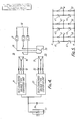
- FIG. 4 of the accompanying drawings shows a schematic block diagram of a conventional widely used power converter device for interconnecting alternating current systems.
- Reference numerals 11, 21 designate three-phase self-commutated voltage type inverter units (hereinbelow called inverter units); 12, 22 designate system interconnecting reactors; 13, 23 designate isolating transformer units; 14, 24 designate windings of transformer units 13, 23; and 15, 25 likewise designate a.c. windings.
- the a.c. windings 15, 25 of transformer units 13, 23 are connected in series in respect of each phase. Their outputs are connected to a.c. systems 32 through a.c. switches 31. In contrast, the d.c. sides of both inverter units 11, 21 have a common d.c. power source 33 having a capacitor 34 connected in parallel therewith.
- Inverter units 11, 21 are started in operation by a signal from a control circuit, not shown.
- the rise of the output voltage of inverter units 11, 21 from zero is made gradual, to avoid excitation rush current in transformer units 13, 23.
- a.c. switches 31 are closed when the amplitude and phase of the resultant voltage of a.c. windings 15, 25 of transformer units 13, 23 coincide with the amplitude and phase of the voltage of systems 32. This is called synchronising.
- a.c. switches 31 are opened simultaneously with cessation of operation of inverter units 11, 21.
- the time between stopping of inverter units 11, 21 and opening of a.c. switches 31 is less than 0.1 second, to avoid the problem to be discussed below.
- Self-commutated inverters for system interconnection have recently begun to be used in systems such as solar generators or fuel cells.
- System interconnection based on self-commutated inverters in the case where the a.c. system is weak, are of superior stability compared with system interconnection based on externally commutated inverters.
- the reason for this is that, in the case of externally commutated inverters, commutation of the thyristors depends on the voltage of the a.c. system, so commutation of the thyristors may be prevented by disturbance of the system voltage, i.e. so-called commutation failure occurs.
- inverter units 11, 21 may be temporarily cut off by generation of a.c. overcurrent if, for example, there is an instantaneous voltage fluctuation of the a.c. system. In this case, it is difficult to restart the operation immediately when the voltage is reset. The reason for this is that a.c. switches 31 must open whenever a.c. overcurrent occurs.
- the excitation characteristic of the iron core is not totally linear, but rather is a non-linear curve having hysteresis. Since, in order to create a sine wave voltage, high frequencies must be contained in the exciting current, if there is some restriction that prevents these high frequencies from flowing, the induced voltage will not be a sine wave.
- the second problem concerns d.c. overvoltage in the steady state.
- the induced voltage is not a simple sine wave, but contains harmonic components. It has been experimentally determined that a peak value of about 2.4 times the root mean square value of the sine wave appears.
- the d.c. voltage of the capacitor 34 was charged up to this value.
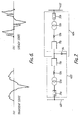
- Figure 6 shows measured waveforms obtained by experiment as described above.
- inverter units 11, 21 are employed.
- this invention is applicable not merely to conversion from d.c. to a.c., but also to reactive power compensator devices, or rectifiers whose power factor can be regulated, so hereinbelow numerals 11, 21 refer generally to self-commutated voltage type converters, and the whole system will be taken as being a power converter device.
- a power converter device comprises a plurality of self-commutated voltage type converters, each connected to a common d.c. circuit; a plurality of transformers, each having d.c. windings and a.c. windings, the d.c. windings being connected to a.c. output terminals of a respective one of the converters and each of the a.c. windings being connected in series; a.c. switch means, through which the serially connected a.c. windings of said transformers are connected to power sytems; and a capacitor provided in said common d.c. circuit; characterised in the provision of a d.c. overvoltage suppression means connected in parallel with said common d.c. circuit, said suppression means comprising a series circuit of a resistor and an interrupter switch means.
- a method of operating the device comprises the steps of starting said converters; opening said interupter switch; and closing said a.c. switch means when the output of the a.c. windings is in synchronism with the power systems; characterised in that temporary stopping of the power converter device is brought about by stopping the operation of the converters and closing the interrupter switch means.
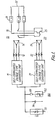
- reference numeral 100 designates a d.c. overvoltage suppression device. This consists of a resistor 101 and circuit breaker device 102.
- Reference numerals 11, 21 designate the self-commutated voltage type converter units.
- FIG. 5 A typical example of self-commutated voltage type converter units 11, 21 is shown in Figure 5.
- reference numerals 41 to 46 designate GTOs, and 47 to 52 designate diodes.
- This inverter circuit has recently been very widely employed, so a detailed description of it will be omitted.
- d.c. power source 33 Before this power converter device is interconnected to the system, with a.c. switch 31 open, first of all d.c. power source 33 is powered up, and self-commutated voltage type converter units 11, 21 are operated.
- the voltage of d.c. power source 33 can be gradually increased by phase control of the thyristor of the thyristor rectifier. Rush current to capacitor 34 is, therefore, restricted.
- the output voltage of self-commutated voltage type converter 11, 21 is gradually raised from 0.
- the methods by which this can be done include the method of gradually starting up d.c. power source 33 and the method of using voltage regulation means of self-commutated voltage type converter units 11, 21 themselves.
- the d.c. windings 15, 25 of the two transformer units 13, 23 are connected in series. Their resultant voltage is controlled by a control device, not shown, so as to coincide, in amplitude and phase, with the system voltage. Once such coincidence is achieved, a.c. switch 31 is closed. That is, synchronising is performed.
- gate (base) blocking of semiconductor switching elements 41 to 46 of self-commutated voltage type converter units 11, 21 is immediately performed.
- circuit breaker 102 is closed.
- a.c. switch 31 is not opened.
- gate (base) blocking is meant that these semiconductor switching elements 41 to 46 are put into the OFF condition, their switching operation being thereby stopped.
- circuit breaker device 102 may appropriately be a semiconductor switching element, such as a GTO.
- the rated capacity of resistor 101 in Figure 1 is preferably low, since a delta connection of transformer d.c. windings 14, 24 has smaller impedance to the third harmonic and the sixth harmonic, etc. In the case of a Y connection, the rated capacity of resistor 101 should be about half the transformer excitation rated capacity.
- control is performed as follows.
- the gate pattern supplied to semiconductor switching elements 11, 21 is found by calculation in a control circuit, and is such that, when they are driven with this gate pattern, the magnitude and phase of the resultant voltage of the transformers coincides with the magnitude and phase of the system voltage.
- This gate pattern effects de-blocking of the gates (bases) of semiconductor switching elements 41 to 46.
- Gate (base) de-blocking means a condition in which the switching action of semiconductor switching elements 41 to 46 is thereby brought about.
- gate (base) de-blocking On gate (base) de-blocking, the output voltage of the self-commutated voltage type converter is applied stepwise to transformer units 13, 23. However, since the transformer units are already excited by the a.c. system, an excess excitsation rush current cannot flow. Breaker 102 is turned off concomitantly with gate (base) de-blocking.
- temporary operation interruption and operation re-starting of the power converter can be carried out by gate (base) blocking and de-blocking of semiconductor switching elements 41 to 46, together with connection and disconnection of circuit breaker 102.
- FIG. 2 shows another embodiment of this invention.
- the difference from Figure 1 is that there is no d.c. power source 33, an auxiliary charging circuit 300 for capacitor 34 being provided instead.
- This type of construction can be applied to a reactive power regulator.
- 300 in the figure is the auxiliary charging circuit.
- Auxiliary charging circuit 300 may consist, for example, as shown in Figure 3, of a.c. switches 301, 306, resistor 302, transformer 303, rectifier 304 and fuse 305.
- capacitor 34 When a.c. switch 301 is closed, capacitor 34 is charged through the path, resistor 302, transformer 303, rectifier 304, and fuse 305. The magnitude of the charging current to capacitor 34 is restricted by resistor 302.
- a.c. switch 306 When capacitor 34 is charged to the prescribed voltage, or when it is charged to practically the prescribed voltage, a.c. switch 306 is opened. After this, as described with reference to Figure 1, the output voltages of self-commutated voltage type converter units 11, 21 are gradually raised, the resultant voltage of a.c. windings 15, 25 of the two transformer units 13, 23 are controlled such as to coincide with the system voltage, and a.c. switch 31 is closed. a.c. switches 301, 306 of the auxiliary charging circuit are then opened.
- d.c. overvoltage prevention device 100 is not used at all in this process. Or rather, if it were used, it would cause insufficiency of the capacity of auxiliary charging circuit 300. The reason why d.c. overvoltage prevention device 100 is needed is to temporarily interrupt operation of the power converter in the condition where a.o. switch 31 is closed. The operation of d.c. overvoltage prevention device 100 is then the same as described above, so an explanation of it is omitted
- E AC k E d f( ⁇ , a,) (1)
- k a constant uniformly determined by the transformation ratio of the transformers, the number of units connected in series, and the mode of inverter unit control (for example, PWM control)
- ⁇ the voltage phase difference between the resultant voltage and the system
- a the control angle (or degree of modulation) of PWM control.
- delta connection of a.c. windings 25 of transformer unit 23 to provide a transformer unit connection to remove specific higher harminics are given in the literature (for example, the delta connection connected as shown at page 172 of "Turnoff Thyristors" compiled by N. Seki, M. Kurada and M. Takeichi, published by Denki Shoin on 20th April, 1983).
- Reactors 12 and 22 in FIGURE 1 and 2 are provided between inverter units 11 and 21 and transformer units 13 and 23. However, this invention could be applied also in the case where they are provided between a.c. switches 31 and transformer units 13 and 23. Specifically, although reactors 12 and 22 have a current limiting effect on transformer units 13 and 23, normally reactors 12 and 22 are at the most about 20%, where 20% indicates the value of percent impedance of reactors 12, 22, which is too small in relation to the approximately 50% value that is needed to achieve the objective of current limitation.
- the d.c. power source referred to here means an irreversible power source such as a thyristor rectifier, fuel cell, or solar cell etc. and does not include an accumulator.
- FIGURE 7 In a system that performs a.c. - d.c. -a.c. conversion, as in the case of a d.c. power transmission system, use of a system as shown in FIGURE 7 may be considered, in which the circuit shown in FIGURE 1 is employed with two d.c. parts in common.
- reference numerals 401 and 401 designate different systems
- 403 and 404 designate power converter devices described in FIGURE 1, and these have their d.c. parts in common.
- this invention can be applied when one of the a.c. switches at both ends is closed. It should be noted that insertion of a resistor in the conventional d.c. circuit was carried out in the following cases:
- the resistor is normally a high resistance, with the objective of discharge, and stays inserted during operation.
- This is similar to the present invention in that resistance is low when discharge in a short time is required during stoppage, or is used only during stoppage.
- the resistance is determined by the capacity of the capacitor and the necessary discharge time, and a short time can be employed.
- the resistance is determined by the excitation capacity of transformers 13 and 23, and the period for which it is applied is unrelated to the resistance.
- FIGURE 1 in this reference shows a power converter system of one MW.
- the output of three unit inverters is connected to a single transformer, so the phenomenon of the voltage distribution between the unit transformers becoming unbalanced when the a.c.
- the aim is to prevent overvoltage generated in the d.c. winding side when inserting a transformer unit in parallel into the system, and to protect the windings and prevent d.c. overvoltage, and also, in the steady state after insertion in parallel in the system, to prevent d.c. overvoltage by suppressing high frequencies generated in the d.c. windings.
Landscapes
- Engineering & Computer Science (AREA)
- Power Engineering (AREA)
- Inverter Devices (AREA)
- Emergency Protection Circuit Devices (AREA)
- Supply And Distribution Of Alternating Current (AREA)
Applications Claiming Priority (2)
| Application Number | Priority Date | Filing Date | Title |
|---|---|---|---|
| JP62330084A JP2645045B2 (ja) | 1987-12-28 | 1987-12-28 | 電力変換装置 |
| JP330084/87 | 1987-12-28 |
Publications (3)
| Publication Number | Publication Date |
|---|---|
| EP0323173A2 true EP0323173A2 (fr) | 1989-07-05 |
| EP0323173A3 EP0323173A3 (en) | 1990-08-22 |
| EP0323173B1 EP0323173B1 (fr) | 1995-10-11 |
Family
ID=18228604
Family Applications (1)
| Application Number | Title | Priority Date | Filing Date |
|---|---|---|---|
| EP88312255A Expired - Lifetime EP0323173B1 (fr) | 1987-12-28 | 1988-12-22 | Dispositif convertisseur d'énergie |
Country Status (5)
| Country | Link |
|---|---|
| US (1) | US4922124A (fr) |
| EP (1) | EP0323173B1 (fr) |
| JP (1) | JP2645045B2 (fr) |
| CA (1) | CA1296054C (fr) |
| DE (1) | DE3854574T2 (fr) |
Families Citing this family (19)
| Publication number | Priority date | Publication date | Assignee | Title |
|---|---|---|---|---|
| JP2714195B2 (ja) * | 1989-12-08 | 1998-02-16 | 株式会社東芝 | 電圧変動及び高調波の抑制装置 |
| US5343080A (en) * | 1991-11-15 | 1994-08-30 | Power Distribution, Inc. | Harmonic cancellation system |
| US5434455A (en) * | 1991-11-15 | 1995-07-18 | Power Distribution, Inc. | Harmonic cancellation system |
| CA2174568C (fr) | 1995-04-21 | 2009-11-17 | Mark A. Runkle | Systeme d'interconnexion pour la transmission d'energie entre systemes electriques |
| US5952816A (en) * | 1995-04-21 | 1999-09-14 | General Electric Co. | Compensation for power transfer systems using variable rotary transformer |
| US5742515A (en) * | 1995-04-21 | 1998-04-21 | General Electric Co. | Asynchronous conversion method and apparatus for use with variable speed turbine hydroelectric generation |
| US5953225A (en) * | 1995-04-21 | 1999-09-14 | General Electric Co. | Power flow control and power recovery with rotary transformers |
| US5841267A (en) * | 1995-04-21 | 1998-11-24 | General Electric Co. | Power flow control with rotary transformers |
| US5677833A (en) * | 1995-05-16 | 1997-10-14 | Raytheon Company | Power conditioning system for a four quadrant photovoltaic array with an inverter for each array quadrant |
| TW336271B (en) * | 1995-06-13 | 1998-07-11 | Sanyo Electric Co | Solar generator and an air conditioner with such a solar generator |
| US5608615A (en) * | 1996-03-11 | 1997-03-04 | Luce; John W. | Asynchronous intergrid transfer apparatus |
| US5896281A (en) * | 1997-07-02 | 1999-04-20 | Raytheon Company | Power conditioning system for a four quadrant photovoltaic array with an inverter for each array quadrant |
| CA2351895C (fr) | 2000-06-30 | 2009-12-15 | General Electric Company | Ensemble de fixation de bague collectrice pour barre haute puissance de frottement de courant triphase |
| US6469414B2 (en) | 2000-06-30 | 2002-10-22 | General Electric Company | Slip-ring mounting assembly for high-power rotary current collector system |
| US6465926B2 (en) | 2000-06-30 | 2002-10-15 | General Electric Company | Cleaning/cooling of high-power rotary current collector system |
| US6456021B1 (en) | 2000-06-30 | 2002-09-24 | General Electric Company | Rotating variable frequency transformer with high voltage cables |
| US7269036B2 (en) * | 2003-05-12 | 2007-09-11 | Siemens Vdo Automotive Corporation | Method and apparatus for adjusting wakeup time in electrical power converter systems and transformer isolation |
| JP2006129571A (ja) * | 2004-10-27 | 2006-05-18 | Fuji Electric Systems Co Ltd | 電力変換装置の初期充電装置 |
| ES2428001T3 (es) * | 2008-11-26 | 2013-11-05 | Abb Technology Ag | Disposición de disyuntor para corriente continua de alto voltaje y método asociado |
Family Cites Families (18)
| Publication number | Priority date | Publication date | Assignee | Title |
|---|---|---|---|---|
| JPS4981833A (fr) * | 1972-12-13 | 1974-08-07 | ||
| US3816809A (en) * | 1973-04-30 | 1974-06-11 | Gte Automatic Electric Lab Inc | Power supply having improved over-voltage protection |
| JPS5159323A (en) * | 1974-11-21 | 1976-05-24 | Mitsubishi Electric Corp | Denryugatainbaatano hogosochi |
| DE2605793C2 (de) * | 1976-02-13 | 1984-09-27 | Brown, Boveri & Cie Ag, 6800 Mannheim | Verfahren zur Inbetriebnahme einer Station einer Hochspannungs-Gleichstrom-Übertragungsanlage (HGÜ) |
| US4251735A (en) * | 1979-07-23 | 1981-02-17 | United Technologies Corporation | Dual speed control circuit for power flow through an inverter |
| FR2481536A1 (fr) * | 1980-04-24 | 1981-10-30 | Jeumont Schneider | Adaptateur pour circuit intermediaire d'un ensemble de convertisseurs statiques |
| JPS5851742A (ja) * | 1981-09-22 | 1983-03-26 | 関西電力株式会社 | 交直変換装置の起動装置 |
| JPS58154395A (ja) * | 1982-03-09 | 1983-09-13 | Mitsubishi Electric Corp | 交流エレベ−タの制御装置 |
| JPS58145046U (ja) * | 1982-03-23 | 1983-09-29 | 株式会社東芝 | インバ−タ装置 |
| US4488200A (en) * | 1982-09-23 | 1984-12-11 | Tokyo Shibaura Denki Kabushiki Kaisha | No-break power supply apparatus |
| JPS5959081A (ja) * | 1982-09-29 | 1984-04-04 | Toshiba Corp | 自励式電力変換装置の起動方式 |
| JPS60160338A (ja) * | 1984-01-26 | 1985-08-21 | 富士電機株式会社 | 系統連系インバ−タの同期投入制御回路 |
| JPS61106031A (ja) * | 1984-10-26 | 1986-05-24 | 株式会社東芝 | 電力変換装置の起動方法 |
| JPS61173636A (ja) * | 1984-12-18 | 1986-08-05 | 三菱電機株式会社 | 電源装置 |
| JPS61157270A (ja) * | 1984-12-28 | 1986-07-16 | Toshiba Corp | 燃料電池用電力変換装置の起動方法 |
| JPH0797910B2 (ja) * | 1985-11-15 | 1995-10-18 | トヨタ自動車株式会社 | ガスタ−ビン発電装置 |
| DE3607519A1 (de) * | 1986-03-07 | 1987-09-10 | Bbc Brown Boveri & Cie | Regelverfahren und regelanordnung fuer einen stromrichterantrieb mit gleichspannungs-zwischenkreis |
| JPS6322130A (ja) * | 1986-07-14 | 1988-01-29 | コパル電子株式会社 | 魚釣り用リ−ル |
-
1987
- 1987-12-28 JP JP62330084A patent/JP2645045B2/ja not_active Expired - Lifetime
-
1988
- 1988-12-22 EP EP88312255A patent/EP0323173B1/fr not_active Expired - Lifetime
- 1988-12-22 DE DE3854574T patent/DE3854574T2/de not_active Expired - Fee Related
- 1988-12-28 CA CA000587084A patent/CA1296054C/fr not_active Expired - Lifetime
- 1988-12-28 US US07/291,160 patent/US4922124A/en not_active Expired - Lifetime
Also Published As
| Publication number | Publication date |
|---|---|
| US4922124A (en) | 1990-05-01 |
| DE3854574T2 (de) | 1996-03-21 |
| DE3854574D1 (de) | 1995-11-16 |
| CA1296054C (fr) | 1992-02-18 |
| EP0323173A3 (en) | 1990-08-22 |
| JP2645045B2 (ja) | 1997-08-25 |
| JPH01174223A (ja) | 1989-07-10 |
| EP0323173B1 (fr) | 1995-10-11 |
Similar Documents
| Publication | Publication Date | Title |
|---|---|---|
| US4890213A (en) | Power converter device having starting circuits and a method for starting the power converter device | |
| EP0323173B1 (fr) | Dispositif convertisseur d'énergie | |
| US9048691B2 (en) | Converters | |
| US6175166B1 (en) | System for mitigating voltage disturbances and interruptions for power distribution applications | |
| Maharjan et al. | Development and verification test of the 6.6-kV 200-kVA transformerless SDBC-based STATCOM using SiC-MOSFET modules | |
| EP3931959B1 (fr) | Cellule de convertisseur élévateur-abaisseur pour convertisseur multiniveau modulaire | |
| WO2013054567A1 (fr) | Dispositif de conversion de puissance | |
| Ichikawa et al. | Development of self-commutated SVC for power system | |
| Ekstrom et al. | HVDC tapping station: power tapping from a DC transmission line to a local AC network | |
| CN216599460U (zh) | 一种压裂机组的变频控制系统及压裂机组 | |
| EP3913781B1 (fr) | Convertisseurs modulaires multiniveaux | |
| Wijaya et al. | Reducing induction motor starting current using magnetic energy recovery switch (MERS) | |
| RU2334349C1 (ru) | Высоковольтный электропривод переменного тока (его варианты) | |
| Rahman | Matrix converter and its probable applications | |
| JP2500926B2 (ja) | 電力変換装置 | |
| Ashtekar et al. | Power quality improvement by using modular multilevel cascade converter based STATCOM | |
| Panfilov et al. | Multifunction AC voltage regulator for connecting an induction motor to alternating power supply | |
| Starostina | Energy Effective Protection Circuits Of The Start-Up Device Against Switching Overvoltage | |
| Abu-Ali et al. | A novel cell-by-cell pre-charging scheme of modular multilevel converters | |
| EP4402786B1 (fr) | Charge d'un convertisseur multiniveau modulaire | |
| Ball et al. | Static power converters of 500 kW or less serving as the relay interface package for nonconventional generators | |
| Lal et al. | Significance of Five Level B inverter for improving power quality of Microgrid | |
| Vyawahare et al. | Study of Forsmark-Type Voltage Transient on Power UPS in Nuclear Power Plants | |
| Sharma et al. | Derived Hybrid Multilevel Topologies for VSC-HVDC Systems | |
| RU2035119C1 (ru) | Преобразователь переменного тока в постоянный |
Legal Events
| Date | Code | Title | Description |
|---|---|---|---|
| PUAI | Public reference made under article 153(3) epc to a published international application that has entered the european phase |
Free format text: ORIGINAL CODE: 0009012 |
|
| 17P | Request for examination filed |
Effective date: 19890109 |
|
| AK | Designated contracting states |
Kind code of ref document: A2 Designated state(s): CH DE LI SE |
|
| PUAL | Search report despatched |
Free format text: ORIGINAL CODE: 0009013 |
|
| AK | Designated contracting states |
Kind code of ref document: A3 Designated state(s): CH DE LI SE |
|
| 17Q | First examination report despatched |
Effective date: 19920723 |
|
| GRAA | (expected) grant |
Free format text: ORIGINAL CODE: 0009210 |
|
| AK | Designated contracting states |
Kind code of ref document: B1 Designated state(s): CH DE LI SE |
|
| REF | Corresponds to: |
Ref document number: 3854574 Country of ref document: DE Date of ref document: 19951116 |
|
| PGFP | Annual fee paid to national office [announced via postgrant information from national office to epo] |
Ref country code: SE Payment date: 19951215 Year of fee payment: 8 |
|
| PLBE | No opposition filed within time limit |
Free format text: ORIGINAL CODE: 0009261 |
|
| STAA | Information on the status of an ep patent application or granted ep patent |
Free format text: STATUS: NO OPPOSITION FILED WITHIN TIME LIMIT |
|
| 26N | No opposition filed | ||
| PG25 | Lapsed in a contracting state [announced via postgrant information from national office to epo] |
Ref country code: SE Effective date: 19961223 |
|
| EUG | Se: european patent has lapsed |
Ref document number: 88312255.8 |
|
| PGFP | Annual fee paid to national office [announced via postgrant information from national office to epo] |
Ref country code: CH Payment date: 20000103 Year of fee payment: 12 |
|
| PG25 | Lapsed in a contracting state [announced via postgrant information from national office to epo] |
Ref country code: LI Free format text: LAPSE BECAUSE OF NON-PAYMENT OF DUE FEES Effective date: 20001231 Ref country code: CH Free format text: LAPSE BECAUSE OF NON-PAYMENT OF DUE FEES Effective date: 20001231 |
|
| REG | Reference to a national code |
Ref country code: CH Ref legal event code: PL |
|
| PGFP | Annual fee paid to national office [announced via postgrant information from national office to epo] |
Ref country code: DE Payment date: 20020109 Year of fee payment: 14 |
|
| PG25 | Lapsed in a contracting state [announced via postgrant information from national office to epo] |
Ref country code: DE Free format text: LAPSE BECAUSE OF NON-PAYMENT OF DUE FEES Effective date: 20030701 |