EP0323218A1 - Elektrolumineszierende Lampenvorrichtungen unter Verwendung von einzellagigen elektrolumineszierenden Stoffen - Google Patents
Elektrolumineszierende Lampenvorrichtungen unter Verwendung von einzellagigen elektrolumineszierenden Stoffen Download PDFInfo
- Publication number
- EP0323218A1 EP0323218A1 EP88312351A EP88312351A EP0323218A1 EP 0323218 A1 EP0323218 A1 EP 0323218A1 EP 88312351 A EP88312351 A EP 88312351A EP 88312351 A EP88312351 A EP 88312351A EP 0323218 A1 EP0323218 A1 EP 0323218A1
- Authority
- EP
- European Patent Office
- Prior art keywords
- layer
- particles
- accordance
- electroluminescent lamp
- phosphor particles
- Prior art date
- Legal status (The legal status is an assumption and is not a legal conclusion. Google has not performed a legal analysis and makes no representation as to the accuracy of the status listed.)
- Ceased
Links
Images
Classifications
-
- H—ELECTRICITY
- H05—ELECTRIC TECHNIQUES NOT OTHERWISE PROVIDED FOR
- H05B—ELECTRIC HEATING; ELECTRIC LIGHT SOURCES NOT OTHERWISE PROVIDED FOR; CIRCUIT ARRANGEMENTS FOR ELECTRIC LIGHT SOURCES, IN GENERAL
- H05B33/00—Electroluminescent light sources
- H05B33/12—Light sources with substantially two-dimensional [2D] radiating surfaces
- H05B33/14—Light sources with substantially two-dimensional [2D] radiating surfaces characterised by the chemical or physical composition or the arrangement of the electroluminescent material, or by the simultaneous addition of the electroluminescent material in or onto the light source
- H05B33/145—Arrangements of the electroluminescent material
-
- H—ELECTRICITY
- H05—ELECTRIC TECHNIQUES NOT OTHERWISE PROVIDED FOR
- H05B—ELECTRIC HEATING; ELECTRIC LIGHT SOURCES NOT OTHERWISE PROVIDED FOR; CIRCUIT ARRANGEMENTS FOR ELECTRIC LIGHT SOURCES, IN GENERAL
- H05B33/00—Electroluminescent light sources
- H05B33/10—Apparatus or processes specially adapted to the manufacture of electroluminescent light sources
-
- H—ELECTRICITY
- H05—ELECTRIC TECHNIQUES NOT OTHERWISE PROVIDED FOR
- H05B—ELECTRIC HEATING; ELECTRIC LIGHT SOURCES NOT OTHERWISE PROVIDED FOR; CIRCUIT ARRANGEMENTS FOR ELECTRIC LIGHT SOURCES, IN GENERAL
- H05B33/00—Electroluminescent light sources
- H05B33/12—Light sources with substantially two-dimensional [2D] radiating surfaces
- H05B33/20—Light sources with substantially two-dimensional [2D] radiating surfaces characterised by the chemical or physical composition or the arrangement of the material in which the electroluminescent material is embedded
-
- Y—GENERAL TAGGING OF NEW TECHNOLOGICAL DEVELOPMENTS; GENERAL TAGGING OF CROSS-SECTIONAL TECHNOLOGIES SPANNING OVER SEVERAL SECTIONS OF THE IPC; TECHNICAL SUBJECTS COVERED BY FORMER USPC CROSS-REFERENCE ART COLLECTIONS [XRACs] AND DIGESTS
- Y10—TECHNICAL SUBJECTS COVERED BY FORMER USPC
- Y10S—TECHNICAL SUBJECTS COVERED BY FORMER USPC CROSS-REFERENCE ART COLLECTIONS [XRACs] AND DIGESTS
- Y10S428/00—Stock material or miscellaneous articles
- Y10S428/917—Electroluminescent
-
- Y—GENERAL TAGGING OF NEW TECHNOLOGICAL DEVELOPMENTS; GENERAL TAGGING OF CROSS-SECTIONAL TECHNOLOGIES SPANNING OVER SEVERAL SECTIONS OF THE IPC; TECHNICAL SUBJECTS COVERED BY FORMER USPC CROSS-REFERENCE ART COLLECTIONS [XRACs] AND DIGESTS
- Y10—TECHNICAL SUBJECTS COVERED BY FORMER USPC
- Y10T—TECHNICAL SUBJECTS COVERED BY FORMER US CLASSIFICATION
- Y10T428/00—Stock material or miscellaneous articles
- Y10T428/25—Web or sheet containing structurally defined element or component and including a second component containing structurally defined particles
- Y10T428/256—Heavy metal or aluminum or compound thereof
Definitions
- This invention relates generally to electroluminescent lamp devices and, more particularly, to such devices which use a substantially single layer, or monolayer, of specially treated particles of electroluminescent material the sizes of which are selected to optimize the luminous efficiency and uniformity in brightness of the lamp in accordance with electric field conditions which are to be applied thereto
- Electroluminescent lamp devices utilize electroluminescent emitting phosphor materials which produce light when a suitable AC electric field is applied thereto.
- Various structures of, and methods for fabricating, such devices are known to the art.
- a typical device for example, a glass or plastic substrate is coated with a transparent or translucent conducting film.
- Exemplary films include thin metallic layers, such as gold or silver, or certain semiconducting oxides, such as stannic oxide, which may be doped with antimony, or indium oxide doped with tin.
- a layer comprising an electroluminescent phosphor, such as zinc sulfide doped with copper and dispersed in a polymeric binder, is then deposited on such film.
- One or more dielectric layers such as a barium titanate pigment dispersed in a polymeric binder, or unpigmented resins are commonly used for this purpose.
- a conductive metallic layer such as silver paint or vacuum deposited aluminum, is applied to such structure to form the device.
- such layers may be applied in reverse order and, in such cases, the substrate is commonly aluminum foil.
- One technique for depositing such electroluminescent phosphor layer is to deposit such phosphor in a purely random fashion, such as by screen printing, spraying or doctor blade coating techniques.
- useful electroluminescent lamp devices can be fabricated using such randomly deposited phosphors, such devices often have undesirable properties which arise from particle agglomeration or clustering and as a result of the mixing and coating processes.
- the phosphor particles often have such masses that they settle out of solution and such settling action, for example, produces a sparse phosphor population density in some regions or variations in population density from region to region arising from the mixing and coating operations, some regions, for example, containing much thicker phosphor particle layers due to the particle agglomeration. Accordingly, a substantially non-uniform particle distribution exists throughout the mixture and often many, sometime relatively large, regions thereof are completely void of phosphor particles.
- the resultant coating thereof when viewed in cross section, is seen to be highly non-uniform in thickness.
- the electrode layer When an electrode material is deposited onto such structure the electrode layer has non-uniform surface characteristics.
- an AC electric field is applied thereto, a substantially non-uniform electric field is produced across the structure and results in both luminous inefficiency in the operation of the device and substantial non-uniformity in brightness over the surface thereof.
- an electroluminescent lamp element has deposited thereon a substantially single layer, or monolayer, or phosphor particles substantially uniformly distributed in a resin binder layer so as to be substantially uniformly distributed within the electric field applied thereto.
- the phosphor particles are pre-classified so as to provide particles the sizes of which are controllably selected to lie within a relatively narrow distribution range of particle sizes.
- Such pre-classified particles are applied by using suitable coating techniques such as cascading, electrostatic spraying, fluidized bed, silk screening or mechanical impingement techniques which can controllably deposit a substantially uniform layer of such controllably sized particles onto the substrate.
- suitable coating techniques such as cascading, electrostatic spraying, fluidized bed, silk screening or mechanical impingement techniques which can controllably deposit a substantially uniform layer of such controllably sized particles onto the substrate.
- the phosphor particles provide a layer which has essentially a uniform thickness effectively equivalent to the average particle thickness and a substantially uniform area density throughout the entire surface without the agglomeration problems normally encountered using prior techniques.
- the pre-classification of such particles can be performed so as to provide particles in various different and relatively narrow size ranges.
- the selection of a particular range of sizes together with the use thereof in forming a monolayer of phosphor particles permits an electroluminescent element to be specifically designed for varying electric field strengths which in particular applications are selected to satisfy known drive conditions so as to produce optimum brightness and luminous efficiency.
- Such device assures uniformity in the electric field which is to be applied across the device and tends to maximize the electroluminescent sites per unit area over the surface of the device, thereby increasing the overall luminous efficiency and uniformity of appearance, as well as the overall brightness thereof. Further, by avoiding the use of multiple or clustered layers of phosphor particles, there is an elimination of the disadvantages which arise because of the phosphor-over-phosphor interfaces which are normally present in many such devices and which adversely affect the efficiency, brightness and uniformity of the illumination that is produced.
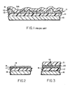
- a typical structure of the prior art comprises a layer 10 of aluminum foil having a thickness lying within a range from .0005-.005 inches.
- a barium titanate dielectric coating 14 is deposited over the aluminum foil surface.
- a mixture 11 comprising electroluminescent phosphor particles 12 dispersed in a resin binder 13 is applied to the surface of the dielectric layer 14. The phosphor particles tend to agglomerate and form clusters thereof, the particles thereby lying on top of one another so as to produce multi-layers of such particles, the thicknesses thereof varying and being equivalent to many particle diameters.
- Such particle agglomerate regions are often non-uniformly dispersed throughout binder 13 so that the thickness of the particle layer varies across the overall surface of the dielectric layer and, in some cases, certain regions 13A thereof may be completely void of phosphor particles.
- An electrode layer 15 is deposited over painted layer 11, layer 15 having relatively highly non-uniform surface characteristics as shown.
- FIG. 2 shows a portion of a layered electroluminescent element in accordance with the invention in which a layer 16 of aluminum foil has deposited on a surface thereof a layer 17 of a dielectric material.
- a material having a relatively high dielectric constant e.g., a barium titanate pigment dispersed in a binder material
- a layer 18 of a resin binder material preferably with a high dielectric constant is deposited on dielectric layer 17 and a substantially single layer, or monolayer, 19 of phosphor particles is uniformly deposited onto the resin binder layer 18.
- the thickness of the binder layer is less than, and preferably about one-half of, the average thickness, or diameter, of the phosphor particles, as shown, although the binder layer thickness may in some cases range from as low as one-quarter to as high as three-quarters of the average thickness of the phosphor particles.
- the selected average particle size will depend upon the application desired, e.g., in terms of the brightness level and the operating conditions expected to be used, e.g., the electric field strengths which are to be used to activate the electroluminescent material.
- the top surfaces of the phosphor particles of the monolayer of particles are generally not covered with the resin binder material and remain exposed.
- the resin binder layer 18 can be applied to the dielectric/aluminum foil element by using suitable machine coating or silk screening techniques known to the art, the thickness thereof being controlled so as to be substantially uniform in nature over the entire surface and to lie within the above discussed desired thickness range.
- the phosphor particles are classified using well known size classification techniques so that their sizes, e.g., effectively the diameters of generally spherical or spherical-like particles, are less than a pre-selected size range so that the particle size distribution lies within a selected relatively narrow range of particle sizes.
- the particles are then controllably applied to the resin binder layer by using well-known cascading, silk screening, fluidized bed, electrostatic spraying or mechanical impingement techniques so that a substantially uniform and dense monolayer 19 thereof is attached to the resin binder layer 18.
- the phosphor particle/resin binder combination is cured using well known curing techniques, such as by evaporation or by chemical reaction.
- a further layer 20 of resin binder is applied over the dried phosphor/binder layer in a substantially uniform coating to a selected thickness which depends upon the desired future use for the electroluminescent lamp in which the element is to be used.
- the layer 20 is applied by using suitable machine coating or silk screening techniques, and again is cured, for example, by suitable solvent evaporation or chemical reaction.
- An electrode layer 21 is then deposited on the layer 20 and has substantially uniform surface characteristics as shown.
- the overall structure shown in FIG. 3 is then ready for use in an electroluminescent (EL) lamp device using well known EL lamp formation techniques.
- EL electroluminescent
- substantially a single layer of phosphor particles having sizes controllably selected to lie within a selected range thereof an uniformly distributed within layers 18 and 20 provides a lamp element with higher luminous efficiency and generally brighter illumination substantially uniformly over the entire lamp emitting region than devices of the prior art using multi-layer particle structures or devices using a monolayer of particles having non-selected or random sizes, which lie in a wide range thereof, as discussed above.
- the brightness of the electroluminescence achieved can be varied by varying the overall thickness of the binder/particle layers 18, 19, 20 and by appropriate selection of the particle sizes. Normally, the smaller the particles, the greater the brightness and the shorter the life of the lamp, while the use of larger particles tends to reduce the brightness and provide longer life.
- the quality of EL lamp devices produced by the invention on a production basis can be maintained to a greater degree than when using such previous lamp forming techniques.
- the particles can be pre-treated before applying them to the resin binder to assure that the tendency to agglomerate will be avoided.
- One effective pre-treatment technique found helpful in this regard is to coat the particles with a suitable material, such as a colloidal silica material, which prevents the clustering thereof.
- a suitable material such as a colloidal silica material, which prevents the clustering thereof.
- a particular material useful for this purpose is available under the trade name "Ludox" from E. I. duPont de Nemours Company of Wilmington, Delaware. When so treated the tendency to agglomerate to any degree is effectively eliminated.
Landscapes
- Engineering & Computer Science (AREA)
- Manufacturing & Machinery (AREA)
- Electroluminescent Light Sources (AREA)
Applications Claiming Priority (2)
| Application Number | Priority Date | Filing Date | Title |
|---|---|---|---|
| US07/139,980 US4902567A (en) | 1987-12-31 | 1987-12-31 | Electroluminescent lamp devices using monolayers of electroluminescent materials |
| US139980 | 1987-12-31 |
Publications (1)
| Publication Number | Publication Date |
|---|---|
| EP0323218A1 true EP0323218A1 (de) | 1989-07-05 |
Family
ID=22489185
Family Applications (1)
| Application Number | Title | Priority Date | Filing Date |
|---|---|---|---|
| EP88312351A Ceased EP0323218A1 (de) | 1987-12-31 | 1988-12-28 | Elektrolumineszierende Lampenvorrichtungen unter Verwendung von einzellagigen elektrolumineszierenden Stoffen |
Country Status (4)
| Country | Link |
|---|---|
| US (1) | US4902567A (de) |
| EP (1) | EP0323218A1 (de) |
| JP (1) | JPH01302692A (de) |
| CA (1) | CA1311517C (de) |
Cited By (7)
| Publication number | Priority date | Publication date | Assignee | Title |
|---|---|---|---|---|
| WO1998053645A1 (en) * | 1997-05-19 | 1998-11-26 | Minnesota Mining And Manufacturing Company | Electroluminescent device and method for producing the same |
| WO1998057525A1 (en) * | 1997-06-12 | 1998-12-17 | Minnesota Mining And Manufacturing Company | Electoluminescent device and method for producing the same |
| US6406803B1 (en) | 1997-05-19 | 2002-06-18 | 3M Innovative Properties Company | Electroluminescent device and method for producing the same |
| US6617784B1 (en) | 1998-06-08 | 2003-09-09 | 3M Innovative Properties Company | Electroluminescent device and method for producing the same |
| EP1244335A3 (de) * | 2001-03-19 | 2004-04-14 | Matsushita Electric Industrial Co., Ltd. | Elektrolumineszente Lampe und Verfahren zur Herstellung derselben |
| EP1416775A1 (de) * | 1999-01-14 | 2004-05-06 | Minnesota Mining And Manufacturing Company | Organisches Elektrolumineszenzelement und Verfahren zu dessen Erzeugung |
| US7695150B2 (en) * | 2005-04-12 | 2010-04-13 | Seiko Instruments Inc. | Lighting unit, display device, and phosphor film |
Families Citing this family (31)
| Publication number | Priority date | Publication date | Assignee | Title |
|---|---|---|---|---|
| EP0541401B1 (de) * | 1991-11-08 | 1997-02-19 | Research Development Corporation Of Japan | Verfahren zur Herstellung einer zweidimensionalen Partikelanordnung |
| DE69310057T2 (de) * | 1992-08-31 | 1997-07-31 | Japan Res Dev Corp | Verfahren und Vorrichtung zur Herstellung einer zweidimensionalen Anordnung aus feiner Teilchen |
| KR100240432B1 (ko) * | 1996-05-22 | 2000-01-15 | 이주현 | 교류 분말 일렉트로루미네센스 소자의 제조 방법 및 소자 구조 |
| US6054809A (en) * | 1996-08-14 | 2000-04-25 | Add-Vision, Inc. | Electroluminescent lamp designs |
| US6011352A (en) * | 1996-11-27 | 2000-01-04 | Add-Vision, Inc. | Flat fluorescent lamp |
| US6153123A (en) | 1997-02-24 | 2000-11-28 | Superior Micropowders, Llc | Sulfur-containing phosphor powders, methods for making phosphor powders and devices incorporating same |
| US6193908B1 (en) * | 1997-02-24 | 2001-02-27 | Superior Micropowders Llc | Electroluminescent phosphor powders, methods for making phosphor powders and devices incorporating same |
| US6199996B1 (en) | 1998-08-26 | 2001-03-13 | Twenty-First Century Technology, Inc. | Low power, low cost illuminated keyboards and keypads |
| US7883227B1 (en) * | 1998-08-26 | 2011-02-08 | Andrew Katrinecz | Low power, low cost illuminated keyboards and keypads |
| WO2000022682A2 (en) * | 1998-10-09 | 2000-04-20 | The Trustees Of Columbia University In The City Of New York | Solid-state photoelectric device |
| US6613455B1 (en) * | 1999-01-14 | 2003-09-02 | 3M Innovative Properties Company | Electroluminescent device and method for producing same |
| DE10005560A1 (de) * | 2000-02-09 | 2001-08-23 | Bosch Gmbh Robert | Flächiges Leuchtelement |
| FR2850677A1 (fr) * | 2003-01-30 | 2004-08-06 | Seb Sa | Fer a pompe electro-osmotique |
| US7777235B2 (en) | 2003-05-05 | 2010-08-17 | Lighting Science Group Corporation | Light emitting diodes with improved light collimation |
| US7157745B2 (en) * | 2004-04-09 | 2007-01-02 | Blonder Greg E | Illumination devices comprising white light emitting diodes and diode arrays and method and apparatus for making them |
| US7633093B2 (en) * | 2003-05-05 | 2009-12-15 | Lighting Science Group Corporation | Method of making optical light engines with elevated LEDs and resulting product |
| US7528421B2 (en) * | 2003-05-05 | 2009-05-05 | Lamina Lighting, Inc. | Surface mountable light emitting diode assemblies packaged for high temperature operation |
| KR100768187B1 (ko) * | 2004-10-26 | 2007-10-17 | 삼성에스디아이 주식회사 | 플라즈마 디스플레이 패널 |
| US8186021B2 (en) * | 2006-01-10 | 2012-05-29 | Csc Group Llc | Conspicuity devices and methods |
| US9775391B1 (en) | 2006-01-10 | 2017-10-03 | Csc Group Llc | Conspicuity devices and methods |
| US10149508B2 (en) | 2006-01-10 | 2018-12-11 | Csc Group Llc | Conspicuity devices and methods |
| US9080764B2 (en) | 2006-01-10 | 2015-07-14 | Csc Group Llc | Conspicuity devices and methods |
| US9951438B2 (en) | 2006-03-07 | 2018-04-24 | Samsung Electronics Co., Ltd. | Compositions, optical component, system including an optical component, devices, and other products |
| JP5773646B2 (ja) | 2007-06-25 | 2015-09-02 | キユーデイー・ビジヨン・インコーポレーテツド | ナノ材料を被着させることを含む組成物および方法 |
| WO2009014707A2 (en) | 2007-07-23 | 2009-01-29 | Qd Vision, Inc. | Quantum dot light enhancement substrate and lighting device including same |
| US8128249B2 (en) * | 2007-08-28 | 2012-03-06 | Qd Vision, Inc. | Apparatus for selectively backlighting a material |
| US8339040B2 (en) | 2007-12-18 | 2012-12-25 | Lumimove, Inc. | Flexible electroluminescent devices and systems |
| US9929325B2 (en) | 2012-06-05 | 2018-03-27 | Samsung Electronics Co., Ltd. | Lighting device including quantum dots |
| USD873163S1 (en) | 2017-09-13 | 2020-01-21 | Csc Group Llc | Conspicuity tag |
| USD860847S1 (en) | 2018-04-23 | 2019-09-24 | Csc Group Llc | Conspicuity device |
| US20250122383A1 (en) * | 2023-10-16 | 2025-04-17 | Meta Platforms Technologies, Llc | Coloring with high effective solar reflectance |
Citations (3)
| Publication number | Priority date | Publication date | Assignee | Title |
|---|---|---|---|---|
| GB967435A (en) * | 1959-09-11 | 1964-08-19 | Corning Glass Works | Electroluminescent cell |
| US4482580A (en) * | 1981-12-14 | 1984-11-13 | Emmett Manley D | Method for forming multilayered electroluminescent device |
| US4529885A (en) * | 1981-12-04 | 1985-07-16 | The Secretary Of State For Defence In Her Britannic Majesty's Government Of The United Kingdom Of Great Britain And Northern Ireland | Direct current electroluminescent devices |
Family Cites Families (4)
| Publication number | Priority date | Publication date | Assignee | Title |
|---|---|---|---|---|
| US4143297A (en) * | 1976-03-08 | 1979-03-06 | Brown, Boveri & Cie Aktiengesellschaft | Information display panel with zinc sulfide powder electroluminescent layers |
| JPS59201392A (ja) * | 1983-04-28 | 1984-11-14 | アルプス電気株式会社 | 分散型エレクトロルミネツセンス素子の製造方法 |
| JPS6081798A (ja) * | 1983-10-13 | 1985-05-09 | アルプス電気株式会社 | 分散型エレクトロルミネツセンス素子 |
| JPS63105493A (ja) * | 1986-10-22 | 1988-05-10 | アルプス電気株式会社 | 薄膜elパネル |
-
1987
- 1987-12-31 US US07/139,980 patent/US4902567A/en not_active Expired - Lifetime
-
1988
- 1988-11-21 CA CA000583602A patent/CA1311517C/en not_active Expired - Lifetime
- 1988-12-19 JP JP63320342A patent/JPH01302692A/ja active Pending
- 1988-12-28 EP EP88312351A patent/EP0323218A1/de not_active Ceased
Patent Citations (3)
| Publication number | Priority date | Publication date | Assignee | Title |
|---|---|---|---|---|
| GB967435A (en) * | 1959-09-11 | 1964-08-19 | Corning Glass Works | Electroluminescent cell |
| US4529885A (en) * | 1981-12-04 | 1985-07-16 | The Secretary Of State For Defence In Her Britannic Majesty's Government Of The United Kingdom Of Great Britain And Northern Ireland | Direct current electroluminescent devices |
| US4482580A (en) * | 1981-12-14 | 1984-11-13 | Emmett Manley D | Method for forming multilayered electroluminescent device |
Non-Patent Citations (1)
| Title |
|---|
| The Philosophical Magazine, Vol. 38, No. 276, January 1947 G. DESTRIAN "The New Phenomenon of Electrophotoluminescence and its Possibilities for the Investigation of Crystal Lattice" pages 700-739 * Totality * * |
Cited By (10)
| Publication number | Priority date | Publication date | Assignee | Title |
|---|---|---|---|---|
| WO1998053645A1 (en) * | 1997-05-19 | 1998-11-26 | Minnesota Mining And Manufacturing Company | Electroluminescent device and method for producing the same |
| US6406803B1 (en) | 1997-05-19 | 2002-06-18 | 3M Innovative Properties Company | Electroluminescent device and method for producing the same |
| WO1998057525A1 (en) * | 1997-06-12 | 1998-12-17 | Minnesota Mining And Manufacturing Company | Electoluminescent device and method for producing the same |
| US6617784B1 (en) | 1998-06-08 | 2003-09-09 | 3M Innovative Properties Company | Electroluminescent device and method for producing the same |
| EP1416775A1 (de) * | 1999-01-14 | 2004-05-06 | Minnesota Mining And Manufacturing Company | Organisches Elektrolumineszenzelement und Verfahren zu dessen Erzeugung |
| EP1244335A3 (de) * | 2001-03-19 | 2004-04-14 | Matsushita Electric Industrial Co., Ltd. | Elektrolumineszente Lampe und Verfahren zur Herstellung derselben |
| US6831411B2 (en) | 2001-03-19 | 2004-12-14 | Matsushita Electric Industrial Co., Ltd. | Electroluminescent lamp having luminescent layer with phosphor particles fixed uniformly |
| US6835112B2 (en) | 2001-03-19 | 2004-12-28 | Matsushita Electric Industrial Co., Ltd. | Electroluminescent lamp and method for manufacturing the same |
| US7695150B2 (en) * | 2005-04-12 | 2010-04-13 | Seiko Instruments Inc. | Lighting unit, display device, and phosphor film |
| CN1873306B (zh) * | 2005-04-12 | 2011-09-14 | 精工电子有限公司 | 照明装置、显示装置和荧光体薄膜 |
Also Published As
| Publication number | Publication date |
|---|---|
| CA1311517C (en) | 1992-12-15 |
| US4902567A (en) | 1990-02-20 |
| JPH01302692A (ja) | 1989-12-06 |
Similar Documents
| Publication | Publication Date | Title |
|---|---|---|
| US4902567A (en) | Electroluminescent lamp devices using monolayers of electroluminescent materials | |
| US4684353A (en) | Flexible electroluminescent film laminate | |
| KR101586506B1 (ko) | 충전제 재료를 포함하는 투명한 전도성 코팅 | |
| US4020389A (en) | Electrode construction for flexible electroluminescent lamp | |
| US2733367A (en) | Electroluminescent lamp structures | |
| US7791273B2 (en) | Electroluminescent light emitting device | |
| EP0830807B1 (de) | Elektrolumineszente lampe mit terpolymer-binder | |
| CN104115561B (zh) | 电致发光装置及其制造 | |
| US6835112B2 (en) | Electroluminescent lamp and method for manufacturing the same | |
| KR20010012691A (ko) | 전자 발광 소자 및 이의 제조 방법 | |
| US3580738A (en) | Plastics materials with conductive surfaces | |
| CN1353567A (zh) | El元件 | |
| EP0202330A1 (de) | Elektrolumineszierende paneele. | |
| JPH08288066A (ja) | 粉末分散型el素子 | |
| JPH06203957A (ja) | 分散型elパネルの製造方法 | |
| JPH11185963A (ja) | エレクトロルミネッセンス | |
| CN121669532A (zh) | 一种具备高介电性能的电致发光器件及其制备方法 | |
| JPH09232076A (ja) | Elランプ | |
| JP2006089594A (ja) | 電場発光蛍光体及びその製造方法、並びにエレクトロルミネッセンス素子 | |
| JPS63283934A (ja) | 光拡散導電性フイルム | |
| JPH06260284A (ja) | 分散型el素子 | |
| JP2003045654A (ja) | Elランプ及びその製造方法 | |
| JPH06124783A (ja) | 分散型el素子 | |
| JPH04277492A (ja) | El素子の製造方法 | |
| JPH05335081A (ja) | 電界発光素子の製造方法 |
Legal Events
| Date | Code | Title | Description |
|---|---|---|---|
| PUAI | Public reference made under article 153(3) epc to a published international application that has entered the european phase |
Free format text: ORIGINAL CODE: 0009012 |
|
| AK | Designated contracting states |
Kind code of ref document: A1 Designated state(s): DE FR GB IT |
|
| 17P | Request for examination filed |
Effective date: 19900105 |
|
| 17Q | First examination report despatched |
Effective date: 19920213 |
|
| STAA | Information on the status of an ep patent application or granted ep patent |
Free format text: STATUS: THE APPLICATION HAS BEEN REFUSED |
|
| 18R | Application refused |
Effective date: 19940924 |