EP0323859A2 - Unité de mémorisation de données dans un système d'identification d'articles - Google Patents
Unité de mémorisation de données dans un système d'identification d'articles Download PDFInfo
- Publication number
- EP0323859A2 EP0323859A2 EP89100283A EP89100283A EP0323859A2 EP 0323859 A2 EP0323859 A2 EP 0323859A2 EP 89100283 A EP89100283 A EP 89100283A EP 89100283 A EP89100283 A EP 89100283A EP 0323859 A2 EP0323859 A2 EP 0323859A2
- Authority
- EP
- European Patent Office
- Prior art keywords
- data
- display
- read
- memory
- storage unit
- Prior art date
- Legal status (The legal status is an assumption and is not a legal conclusion. Google has not performed a legal analysis and makes no representation as to the accuracy of the status listed.)
- Pending
Links
Images


Classifications
-
- G—PHYSICS
- G06—COMPUTING OR CALCULATING; COUNTING
- G06K—GRAPHICAL DATA READING; PRESENTATION OF DATA; RECORD CARRIERS; HANDLING RECORD CARRIERS
- G06K19/00—Record carriers for use with machines and with at least a part designed to carry digital markings
- G06K19/06—Record carriers for use with machines and with at least a part designed to carry digital markings characterised by the kind of the digital marking, e.g. shape, nature, code
- G06K19/067—Record carriers with conductive marks, printed circuits or semiconductor circuit elements, e.g. credit or identity cards also with resonating or responding marks without active components
- G06K19/07—Record carriers with conductive marks, printed circuits or semiconductor circuit elements, e.g. credit or identity cards also with resonating or responding marks without active components with integrated circuit chips
- G06K19/077—Constructional details, e.g. mounting of circuits in the carrier
- G06K19/07701—Constructional details, e.g. mounting of circuits in the carrier the record carrier comprising an interface suitable for human interaction
- G06K19/07703—Constructional details, e.g. mounting of circuits in the carrier the record carrier comprising an interface suitable for human interaction the interface being visual
-
- G—PHYSICS
- G06—COMPUTING OR CALCULATING; COUNTING
- G06K—GRAPHICAL DATA READING; PRESENTATION OF DATA; RECORD CARRIERS; HANDLING RECORD CARRIERS
- G06K19/00—Record carriers for use with machines and with at least a part designed to carry digital markings
- G06K19/06—Record carriers for use with machines and with at least a part designed to carry digital markings characterised by the kind of the digital marking, e.g. shape, nature, code
- G06K19/067—Record carriers with conductive marks, printed circuits or semiconductor circuit elements, e.g. credit or identity cards also with resonating or responding marks without active components
- G06K19/07—Record carriers with conductive marks, printed circuits or semiconductor circuit elements, e.g. credit or identity cards also with resonating or responding marks without active components with integrated circuit chips
- G06K19/0723—Record carriers with conductive marks, printed circuits or semiconductor circuit elements, e.g. credit or identity cards also with resonating or responding marks without active components with integrated circuit chips the record carrier comprising an arrangement for non-contact communication, e.g. wireless communication circuits on transponder cards, non-contact smart cards or RFIDs
-
- G—PHYSICS
- G06—COMPUTING OR CALCULATING; COUNTING
- G06K—GRAPHICAL DATA READING; PRESENTATION OF DATA; RECORD CARRIERS; HANDLING RECORD CARRIERS
- G06K19/00—Record carriers for use with machines and with at least a part designed to carry digital markings
- G06K19/06—Record carriers for use with machines and with at least a part designed to carry digital markings characterised by the kind of the digital marking, e.g. shape, nature, code
- G06K19/067—Record carriers with conductive marks, printed circuits or semiconductor circuit elements, e.g. credit or identity cards also with resonating or responding marks without active components
- G06K19/07—Record carriers with conductive marks, printed circuits or semiconductor circuit elements, e.g. credit or identity cards also with resonating or responding marks without active components with integrated circuit chips
- G06K19/077—Constructional details, e.g. mounting of circuits in the carrier
- G06K19/07749—Constructional details, e.g. mounting of circuits in the carrier the record carrier being capable of non-contact communication, e.g. constructional details of the antenna of a non-contact smart card
- G06K19/07758—Constructional details, e.g. mounting of circuits in the carrier the record carrier being capable of non-contact communication, e.g. constructional details of the antenna of a non-contact smart card arrangements for adhering the record carrier to further objects or living beings, functioning as an identification tag
Definitions
- This invention relates to a data storage unit used in an identification system in which articles such as tools or pallets are to be identified.
- a data storage unit referred to as a "data carrier” having an internal semiconductor memory such as an EE PROM or SRAM is affixed to a travelling article to be identified (a tool or a conveyed part), while a read/write control controller is disposed on a conveyor line and is approached by the conveyed article bearing the data storage unit.
- a read/write control controller is disposed on a conveyor line and is approached by the conveyed article bearing the data storage unit.
- the data storage unit is not equipped with a display function.
- the data storage unit should be provided with a display device for displaying the data.
- a display device for displaying the data.
- merely providing the storage unit with a display device that remains lit at all times results in excessive power consumption by the device. If the device is of the type that has an internal battery, therefore, the battery will be expended in short order and the service life of the data storage unit will be greatly curtailed.
- the present invention has been devised in view of the foregoing problems and its object is to provide a data storage unit in which the data stored in a memory can be visually confirmed from outside the unit without shortening the service life of the unit.
- the present invention relates to an identification system comprising a read/write control unit, and a data storage unit affixed to an article to be identified and having an internal memory for storing identification data which identifies the article, wherein data in the internal memory is read out of the memory or data is written into the memory in response to control performed by the read/write control unit.
- the data storage unit includes a display device for displaying the data, and display control means for activating the display device only for a predetermined period of time when required.
- the data is displayed on the display device when memory read processing or write processing is performed by the read/write control unit, at at any other time when display is required. This makes it possible for the operator to distinguish the data storage unit itself merely by looking at the display. Moreover, the display is presented only for a prescribed period of time by actuating means which includes a timer, switch or the like, by way of example. Since the display device does not remain activated at all times, power consumed by the display is minimized.
- Fig. 2 is a block diagram illustrating the arrangement of an article identification system to which the present invention is applied.
- the article identification system comprises a host computer 1, a read/write control unit 4 which includes a controller 2 and a read/write head 3, and a data carrier 5 affixed to an article 6 to be identified.
- the article identification system is such that, in response to a command from the host computer 1, the controller 2 accesses the memory of the data carrier 5 via the read/write head 3 to read or write data.
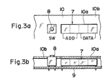
- the data carrier 5 is of a rectangular type, as shown in Fig. 1a, and is equipped with a four-digit digital display device 7 which displays a two-digit address and two-digit data, and a display selection switch 8 for activating and deactivating the display device 7.
- the data carrier 5 is not limited to that of a rectangular type, and other configurations can be employed depending upon the type of article 6 to be identified.
- One example is a cylindrical-type data carrier of the kind shown in Fig. 1b.
- the digital display device 7 and display selection switch 8 are mounted on a printed circuit board 9 within the data carrier 5. Also, though not illustrated in Fig. 3b, other circuit components are mounted on the board and molded in resin along with a battery. In order to render the structure waterproof and exposure-proof, only the portion 10a at which the display device 7 is disposed is transparent, as shown in Figs. 3a and 3b, and the remaining portion 10b is covered with an opaque sheet 10.
- the display selection switch 8 employs a push-button in the illustrated embodiment, the invention is not limited thereto, for a switch of another type, such as a touch switch using a strip of electrically conductive rubber, can be adopted as the display selection switch.
- the digital display device 7 is activated to produce a display only for a fixed period of time when read or write processing is executed or only when the display selection switch 8 is pressed; at all other times the digital display device 7 is in the deactivated state and does not produce a display.
- Fig. 4 is a block diagram illustrating the circuit arrangement of the data carrier 5.
- the circuitry of the data carrier 5 comprises a demodulator circuit 11 for demodulating a transmitted command from the read/write head 3 in contactless, electromagnetic fashion; a decoding circuit 12 for converting the demodulated signal into a digital signal; a command decoder 13 which receives the digital signal and decodes the command; a data register 14 for subjecting the digital signal obtained at reception to a serial-to-parallel conversion, and for subjecting response data transmitted in the direction of the read/write head 3 to a parallel-to-serial conversion; a read/write control circuit 15 which, in response to a command-normal output decoded by the command decoder 13, and in accordance with the on/off state of the display selection switch 8, outputs a corresponding control signal; a memory 16 which, in response to the control signal from the read/write control circuit 15, writes data from the data register 14 into an address designated by the control cicuit 15 or reads data from a
- the format of the command transmitted by the controller 2 and received via the read/write head 3 is as follows: The data is included along with a write command only and not with a read command.
- the format of a response returned from the data carrier 5 to the controller 2 is as follows: Here the data is included along with a read response only and not with a write response.
- Control signals delivered by the read/write control circuit 15 include a five-second timer signal applied to the display timing generator circuit 23 and a read/write signal applied to the memory 16 and status register 20.
- the read/write control circuit 15 applies address signals A0 - A10 to the memory 16 and status register 20.
- the data in the status register 20 is transferred to the data register 14 and memory 16 via a data bus, data is written from the data register 14 to the memory 16 via the data bus, and data is read from memory 16 to data register 14 via the data bus.
- the command is received and fed into the command decoder 13 via the demodulator circuit 11 and decoding circuit 12 and is decoded by the decoder 13.
- the read/write control circuit 15 starts the five-second timer, in response to which the display timing generator circuit 23 is actuated.
- the command is a write command
- the write data stored in the data register 14 is written into the memory 16 at the address designated by the read/write control circuit 15.
- the write data in the data register 14 is transferred to and stored in the display data register 21.
- the data in the display data register 21 is displayed on the display device 7 until the next new command arrives.
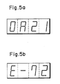
- An example of a display is shown in Fig. 5a. In this example, the data "21" is written at address "OA".
- the five-second timer is reset and the display device continues presenting a display. However, if no command arrives even after five seconds of time passes, the five-second timer runs out of time and the display timing generator circuit 23 is deactivated, thereby deactivating the display device 7.
- an address of the memory 16 is designated by the read/write control circuit 15 and the data stored at this address is read.
- a read response which includes the read data, is transmitted to the side of controller 2 via the data register 14, encoding circuit 24 and modulator circuit 25.
- the read data prevailing at this time is transferred from the data register 14 to the display data register 21, where the data is stored.
- the data is displayed on the display device 7 in the manner set forth above.
- the operation of the five-second timer is the same as in the case of write processing, so that the read data is displayed on the display device 7 for five seconds.
- the memory 16 is not subjected to read/write processing, in which case an error code corresponding to the error mode is read out of the error code storing circuit 17 and transferred to the display data register 21, where the error code is stored.
- the code is displayed on the display device 7. An example of this display is shown in Fig. 5b. In this example, "E” indicating an error is displayed, along with an error code "72".
- the read/write control circuit 15 responds by designating the leading address of the memory 16 and applying a switch operation signal to the display timing generator circuit 23 to place the latter in operation.
- the data at the designated or leading address of the memory 16 is read and transferred, for storage, to the display data register 21 via the data register 14.
- the data in the display data register 21 is displayed on the display device 7. This display continues as long as the display selection switch 8 is closed.
- the display timing generator circuit 23 is deactivated and, hence, the display is extinguished.
- the address of memory 16 is successively incremented so that the data in memory 16 is sequentially read and displayed on the display device 7.
- the operator is capable of directly reading the contents in memory 16 of data carrier 5 at any time.
- the battery level sensing circuit 19 which responds by applying an alarm signal to the display timing generator circuit 23.
- the latter changes the display timing period conforming to the alarm signal during operation of the display, thereby blanking the display presented on the display device 7. In other words, the display is made to flash.
- the flashing display notifies the operator of the fact that the battery of the data carrier is approaching the ends of its service life.
- a data storage unit is equipped with a data display device.
- a data display device This makes it possible to visually confirm read or written data and to distinguish among a plurality of articles to be identified even when the articles have the same external shape and the same color. Likewise, it is possible to distinguish among data storage units having the same external shape.
- the storage unit is provided with means for activating the data display device only for a prescribed period of time when necessary. When display is not required, therefore, the data display device is extinguished. This feature makes it possible to obtain the above-described visual confirmation function while minimizing power consumption.
Landscapes
- Engineering & Computer Science (AREA)
- Computer Hardware Design (AREA)
- Microelectronics & Electronic Packaging (AREA)
- Physics & Mathematics (AREA)
- General Physics & Mathematics (AREA)
- Theoretical Computer Science (AREA)
- Computer Networks & Wireless Communication (AREA)
- Maintenance And Management Of Digital Transmission (AREA)
- Control Of Indicators Other Than Cathode Ray Tubes (AREA)
Applications Claiming Priority (2)
| Application Number | Priority Date | Filing Date | Title |
|---|---|---|---|
| JP63001295A JPH01177746A (ja) | 1988-01-08 | 1988-01-08 | データ通信装置 |
| JP1295/88 | 1988-01-08 |
Publications (1)
| Publication Number | Publication Date |
|---|---|
| EP0323859A2 true EP0323859A2 (fr) | 1989-07-12 |
Family
ID=11497473
Family Applications (1)
| Application Number | Title | Priority Date | Filing Date |
|---|---|---|---|
| EP89100283A Pending EP0323859A2 (fr) | 1988-01-08 | 1989-01-09 | Unité de mémorisation de données dans un système d'identification d'articles |
Country Status (2)
| Country | Link |
|---|---|
| EP (1) | EP0323859A2 (fr) |
| JP (1) | JPH01177746A (fr) |
Cited By (8)
| Publication number | Priority date | Publication date | Assignee | Title |
|---|---|---|---|---|
| EP0467497A1 (fr) * | 1990-07-17 | 1992-01-22 | Mitsubishi Denki Kabushiki Kaisha | Carte à circuit intégré |
| WO1996027853A1 (fr) * | 1995-03-08 | 1996-09-12 | Vincent Peyronnet | Procede de marquage d'identification |
| US5684705A (en) * | 1994-08-12 | 1997-11-04 | Neopost Limited | Mailing system |
| WO1999005644A3 (fr) * | 1997-07-25 | 1999-04-08 | Aventis Res & Tech Gmbh & Co | Carte a puce dotee d'un affichage avec possibilite de memorisation temporaire sur la base d'un affichage a matrice active |
| FR2772166A1 (fr) * | 1997-12-10 | 1999-06-11 | Schlumberger Ind Sa | Dispositif antivol pour un ticket electronique de stationnement payant |
| EP1022065A3 (fr) * | 1999-01-25 | 2004-08-11 | Pitney Bowes Inc. | Marque électronique et méthodes d'utilisation dans des procédés postaux |
| EP2081112A2 (fr) | 2008-01-17 | 2009-07-22 | MariSense Oy | Agencement pour indiquer les états anormaux pour unités d'affichage d'informations |
| EP1697811A4 (fr) * | 2003-09-03 | 2009-11-11 | Visible Tech Knowledgy Inc | Afficheur et etiquette actualisable par voie electronique |
-
1988
- 1988-01-08 JP JP63001295A patent/JPH01177746A/ja active Pending
-
1989
- 1989-01-09 EP EP89100283A patent/EP0323859A2/fr active Pending
Cited By (10)
| Publication number | Priority date | Publication date | Assignee | Title |
|---|---|---|---|---|
| EP0467497A1 (fr) * | 1990-07-17 | 1992-01-22 | Mitsubishi Denki Kabushiki Kaisha | Carte à circuit intégré |
| US5684705A (en) * | 1994-08-12 | 1997-11-04 | Neopost Limited | Mailing system |
| WO1996027853A1 (fr) * | 1995-03-08 | 1996-09-12 | Vincent Peyronnet | Procede de marquage d'identification |
| WO1999005644A3 (fr) * | 1997-07-25 | 1999-04-08 | Aventis Res & Tech Gmbh & Co | Carte a puce dotee d'un affichage avec possibilite de memorisation temporaire sur la base d'un affichage a matrice active |
| FR2772166A1 (fr) * | 1997-12-10 | 1999-06-11 | Schlumberger Ind Sa | Dispositif antivol pour un ticket electronique de stationnement payant |
| EP0923053A1 (fr) * | 1997-12-10 | 1999-06-16 | SCHLUMBERGER Systèmes | Dispositif antivol pour un ticket électronique de stationnement payant |
| EP1022065A3 (fr) * | 1999-01-25 | 2004-08-11 | Pitney Bowes Inc. | Marque électronique et méthodes d'utilisation dans des procédés postaux |
| EP1697811A4 (fr) * | 2003-09-03 | 2009-11-11 | Visible Tech Knowledgy Inc | Afficheur et etiquette actualisable par voie electronique |
| EP2081112A2 (fr) | 2008-01-17 | 2009-07-22 | MariSense Oy | Agencement pour indiquer les états anormaux pour unités d'affichage d'informations |
| EP2081112A3 (fr) * | 2008-01-17 | 2010-04-28 | MariSense Oy | Agencement pour indiquer les états anormaux pour unités d'affichage d'informations |
Also Published As
| Publication number | Publication date |
|---|---|
| JPH01177746A (ja) | 1989-07-14 |
Similar Documents
| Publication | Publication Date | Title |
|---|---|---|
| KR0144192B1 (ko) | 믹의 리드기능을 갖는 리모콘 송신기 및 이의 믹 내용 디스플레이방법 | |
| EP0254517B1 (fr) | Dispositif pour l'enregistrement de programmes pour appareils électroniques | |
| AU694418B2 (en) | Portable work station and data collection terminal including switchable multi-purpose touch screen display | |
| KR940002359B1 (ko) | 식별 시스템용 프로그래머 | |
| EP0323859A2 (fr) | Unité de mémorisation de données dans un système d'identification d'articles | |
| JPH03282581A (ja) | 価格表示システム及びそれに関連する方法 | |
| EP0981810A4 (fr) | Lecteur pour systeme d'identification de radio-frequences | |
| EP0899677A3 (fr) | Dispositif de lecture pour un système électronique d'identification | |
| US5278399A (en) | Data entry unit | |
| CA1296066C (fr) | Recepteur de radiomessagerie a protection des messages | |
| US5373146A (en) | Card based access system with reader updating of the memory | |
| AU649098B2 (en) | IC card information read/write system | |
| JP2674831B2 (ja) | 表示機能付携帯無線装置 | |
| GB2185134A (en) | Memory package | |
| GB2284689A (en) | Programming SMART cards. | |
| US20020175807A1 (en) | Identification device | |
| SE8504092D0 (sv) | Datainsamlingsterminal | |
| JP3642124B2 (ja) | 光学式読取装置および置き台 | |
| JPS6234292A (ja) | Icカ−ド装置 | |
| JPH076193A (ja) | バーコード信号発生器 | |
| JPS56108108A (en) | Sequence control system | |
| US6508401B1 (en) | Aerospatiale matra airbus | |
| JPS6349893A (ja) | バ−コ−ド読み取り装置 | |
| GB2156128A (en) | Electronic guard patrol systems | |
| JPH1062557A (ja) | タ グ |
Legal Events
| Date | Code | Title | Description |
|---|---|---|---|
| PUAI | Public reference made under article 153(3) epc to a published international application that has entered the european phase |
Free format text: ORIGINAL CODE: 0009012 |
|
| 17P | Request for examination filed |
Effective date: 19890109 |
|
| AK | Designated contracting states |
Kind code of ref document: A2 Designated state(s): AT BE CH DE ES FR GB GR IT LI NL SE |
|
| 18W | Application withdrawn |
Withdrawal date: 19911121 |
|
| D18W | Application withdrawn (deleted) | ||
| STAA | Information on the status of an ep patent application or granted ep patent |
Free format text: STATUS: THE APPLICATION HAS BEEN WITHDRAWN |
|
| R18W | Application withdrawn (corrected) |
Effective date: 19911121 |
|
| D18W | Application withdrawn (deleted) | ||
| 18D | Application deemed to be withdrawn |
Effective date: 19910801 |
|
| R18W | Application withdrawn (corrected) |
Effective date: 19911114 |