EP0324381A2 - Dérivation automatique - Google Patents
Dérivation automatique Download PDFInfo
- Publication number
- EP0324381A2 EP0324381A2 EP89100174A EP89100174A EP0324381A2 EP 0324381 A2 EP0324381 A2 EP 0324381A2 EP 89100174 A EP89100174 A EP 89100174A EP 89100174 A EP89100174 A EP 89100174A EP 0324381 A2 EP0324381 A2 EP 0324381A2
- Authority
- EP
- European Patent Office
- Prior art keywords
- switch
- signal
- input
- bypass
- differential amplifier
- Prior art date
- Legal status (The legal status is an assumption and is not a legal conclusion. Google has not performed a legal analysis and makes no representation as to the accuracy of the status listed.)
- Withdrawn
Links
- 239000003990 capacitor Substances 0.000 claims description 4
- 238000004804 winding Methods 0.000 claims description 3
- 230000002950 deficient Effects 0.000 abstract 1
- 238000009434 installation Methods 0.000 abstract 1
- 230000008054 signal transmission Effects 0.000 abstract 1
- 230000005540 biological transmission Effects 0.000 description 5
- 230000008859 change Effects 0.000 description 3
- 230000035945 sensitivity Effects 0.000 description 3
- 230000009471 action Effects 0.000 description 1
- 230000002730 additional effect Effects 0.000 description 1
- 230000008901 benefit Effects 0.000 description 1
- 238000012505 colouration Methods 0.000 description 1
- 230000007547 defect Effects 0.000 description 1
- 238000010586 diagram Methods 0.000 description 1
- 230000000694 effects Effects 0.000 description 1
- 238000005516 engineering process Methods 0.000 description 1
- 230000007257 malfunction Effects 0.000 description 1
- 230000001105 regulatory effect Effects 0.000 description 1
- 230000007704 transition Effects 0.000 description 1
Images
Classifications
-
- H—ELECTRICITY
- H04—ELECTRIC COMMUNICATION TECHNIQUE
- H04B—TRANSMISSION
- H04B1/00—Details of transmission systems, not covered by a single one of groups H04B3/00 - H04B13/00; Details of transmission systems not characterised by the medium used for transmission
- H04B1/74—Details of transmission systems, not covered by a single one of groups H04B3/00 - H04B13/00; Details of transmission systems not characterised by the medium used for transmission for increasing reliability, e.g. using redundant or spare channels or apparatus
- H04B1/745—Details of transmission systems, not covered by a single one of groups H04B3/00 - H04B13/00; Details of transmission systems not characterised by the medium used for transmission for increasing reliability, e.g. using redundant or spare channels or apparatus using by-passing or self-healing methods
Definitions
- the invention relates to an automatic bypass, which is used in television studio technology during broadcasting or for securing in error situations in the television transmission path, for example for signal-processing linear devices (noise-reducing, introductory, correcting and the like), in which the low-frequency and within certain limits the medium-frequency energy of the signals does not change significantly.
- An automatic bypass of the type described in the preamble of claim 1 is already known from the catalog of the company Philips, PTV Professional Television Measuring Equipment, 1986 - 1987, p. 109.
- a disadvantage of the known bypass is that it only fully or partially responds when the voltage of the processing unit is switched off, the change in the parameters of the output signal, for example if the operation deteriorates due to the defect or the output signal is switched off, not taken into account.
- Another disadvantage of the known bypass is the possibility that it can be switched several times in an unstable manner if the supply is unstable or is interrupted, making the transmission of the signal impossible.
- the object of the invention is to create an automatic bypass with expanded functional possibilities.
- the state of the parameters of the signals is to be monitored and, in the case of unstable operation, including an unstable voltage, a transition to a stable switched-on state, so that uninterrupted transmission of the signal is ensured.
- a preferred development of the automatic bypass according to the invention is the subject of claim 2.
- the advantage of the bypass according to the invention is its expanded functional possibilities.
- the main parameters of the output signal including the constant component of the signal with reduced level and ⁇ -distortions are constantly monitored.
- the device is switched off stably and switched to the bypass operating state when certain values of the monitored parameters or the supply voltage are changed.
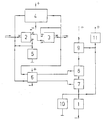
- the automatic bypass contains an electromagnetic relay 1 with a first and a second contact changeover switch 2 or 3.
- the movable contact 2.0 of the first contact changeover switch 2 is connected to the signal input, its normally open contact 2.1 is connected to the input of a processing unit 4 and to ground connected load 5 of the input line 4 and connected to the ground load 5 of the input line.
- the normally closed contact 2.2 of the changeover switch 2 is connected to the normally closed contact 3.2 of the second contact changeover switch 3, the normally open contact 3.1 of which is connected to the signal output of the processing unit 4 and the movable contact 3.0 of which is connected to the output of the automatic bypass.
- the coil of relay 1 is connected to the positive and negative poles of the supply voltage source.
- the normally open contact 2.1 of the first switch 2 is connected to one of the two inputs of a two-stage differential amplifier 6 with differential outputs, the second input of which is connected to the signal output of the processing unit 4.
- the two differential outputs of the differential amplifier 6 are connected to the control inputs of two electronic switches 7 and 8.
- the positive pole of the supply voltage source is connected to the coil of the relay 1 via a series circuit comprising a voltage transformer 9 and the two electronic switches 8, 7.
- the first electronic switch is connected to the control input of the voltage transformer 9 and to ground via a capacitor 10.
- An automatic switch-on unit 11 is located between the positive pole of the supply voltage source and the control input of the voltage transformer 9.
- the automatic bypass according to the invention works as follows:
- the relay 1 When the processing unit 4 is in perfect operating condition, the relay 1 is switched on and the input signal is conducted to the input of the processing unit 4 via the work contacts 2.0 - 2.1 and 3.0 - 3.1.
- the output of the processing unit is an output of the automatic bypass.
- the inputs of the differential amplifier 6 are connected to the input or output of the processing unit 4. If the input and the output signal of the processing unit 4 are the same, the outputs of the differential amplifier 6 carry the same and constant voltages. These voltages and the positive supply voltage transformed by the translator 9 keep the electronic switches 7 and 8 in the switched-on state, the relay 1 being live and the working contacts of the contact switches 2, 3 closed.
- the control voltages of the electronic switches 7 and 8 change in the direction of switching off the first electronic switch 7 and the switched-on state of the second electronic switch 8 or vice versa - switching off the second and switching on the first electronic Switch 8 or 7. If the difference between the input and output signal exceeds a certain value, then depending on its Sign of one of the two electronic changeover switches 7, 8 is switched off, so that the relay 1 is de-energized and the control input of the translator 9 is supplied with a negative voltage via the winding of the relay 1.
- the differential amplifier 6 must have the characteristics of a low-pass filter with a cutting frequency of approximately 2 MHz, which means that it is insensitive to differences outside the pass band and normal function is ensured.
- the delay between the output and the input signal of the processing unit 4 results in significant differences in amplitude, in particular in the case of signals with a dynamic range in brightness, which causes voltage peaks in the closed electronic switches 7 and 8.
- the influence is even stronger due to a more substantial functional difference, eg when introducing graphical information, letters and others into the processing unit 4.
- the potential at the relay is maintained by the integrating action of the capacitor 10, which at the same time the maintains normal operating state of the translator 9.
- the required sensitivity of the automatic bypass can be selected by a suitable choice of the capacitor 10.
- the capacitance has a relatively weak effect on the sensitivity of the DC input-output levels and the low-frequency components of the signal, which make up the largest part of the signal energy and are decisive for the control of the parameters listed above, for example.
- the sensitivity can be regulated by determining the transmission factor of the differential amplifier 6. If there is a natural difference between the input direct current level and the fixing level 0 in the processing unit 4, this difference can be compensated for beforehand by shifting the operating point of the differential amplifier 6.
- the automatic bypass function is maintained when the supply voltage is switched off or fluctuates.
- Automatic switch-on is ensured by the automatic switch-on unit 11, which comes into operation when the device is initially put into operation.
- the switch-on unit 11 supplies the control input of the translator 9 with a high positive potential until the electronic ones Switches 7 and 8 are switched on, after which they become ineffective due to their own time constant.
- the automatic bypass can be controlled manually as follows: repeated switching on in the processing mode - working state by a short contact between the input and output of the translator 9, by switching off the automatic comparison of the signals by switching on the positive supply voltage via a series resistor to relay 1 and by switching off the function of the processing unit 4 by interrupting the negative pole of the supply voltage source to the relay 1 (these functions are not shown in the figure).
- the voltage translator 9 is preferably designed as an NPN transistor connected as an emitter follower, and the electronic changeover switches 7 and 8 are preferably PNP transistors. A reverse polar combination of these elements is possible.
Landscapes
- Engineering & Computer Science (AREA)
- Computer Networks & Wireless Communication (AREA)
- Signal Processing (AREA)
- Amplifiers (AREA)
- Studio Circuits (AREA)
Applications Claiming Priority (2)
| Application Number | Priority Date | Filing Date | Title |
|---|---|---|---|
| BG82604/88 | 1988-01-12 | ||
| BG82604A BG47638A1 (en) | 1988-01-12 | 1988-01-12 | Automatic by- pass |
Publications (1)
| Publication Number | Publication Date |
|---|---|
| EP0324381A2 true EP0324381A2 (fr) | 1989-07-19 |
Family
ID=3920002
Family Applications (1)
| Application Number | Title | Priority Date | Filing Date |
|---|---|---|---|
| EP89100174A Withdrawn EP0324381A2 (fr) | 1988-01-12 | 1989-01-05 | Dérivation automatique |
Country Status (5)
| Country | Link |
|---|---|
| US (1) | US4975801A (fr) |
| EP (1) | EP0324381A2 (fr) |
| JP (1) | JPH01288072A (fr) |
| BG (1) | BG47638A1 (fr) |
| HU (1) | HUT49021A (fr) |
Cited By (3)
| Publication number | Priority date | Publication date | Assignee | Title |
|---|---|---|---|---|
| US5407792A (en) * | 1993-04-10 | 1995-04-18 | E. I. Du Pont De Nemours And Company | Photosensitive silver halide recording material with reduced pressure sensitivity |
| WO1997013331A1 (fr) * | 1995-10-04 | 1997-04-10 | Allgon Ab | Dispositif de derivation dans une unite d'amplification |
| RU2153786C1 (ru) * | 1999-01-15 | 2000-07-27 | Военный университет связи | Дублированная система с динамической задержкой |
Family Cites Families (3)
| Publication number | Priority date | Publication date | Assignee | Title |
|---|---|---|---|---|
| JPS5854673B2 (ja) * | 1977-04-15 | 1983-12-06 | 日立工機株式会社 | 印字マグネツト駆動装置 |
| US4291356A (en) * | 1979-08-02 | 1981-09-22 | H.O.P. Consulab Inc. | Apparatus for analyzing a physical quantity |
| JPH0510513Y2 (fr) * | 1985-10-21 | 1993-03-15 |
-
1988
- 1988-01-12 BG BG82604A patent/BG47638A1/xx unknown
-
1989
- 1989-01-05 EP EP89100174A patent/EP0324381A2/fr not_active Withdrawn
- 1989-01-09 US US07/295,259 patent/US4975801A/en not_active Expired - Fee Related
- 1989-01-12 HU HU89105A patent/HUT49021A/hu unknown
- 1989-01-12 JP JP1003872A patent/JPH01288072A/ja active Pending
Cited By (4)
| Publication number | Priority date | Publication date | Assignee | Title |
|---|---|---|---|---|
| US5407792A (en) * | 1993-04-10 | 1995-04-18 | E. I. Du Pont De Nemours And Company | Photosensitive silver halide recording material with reduced pressure sensitivity |
| WO1997013331A1 (fr) * | 1995-10-04 | 1997-04-10 | Allgon Ab | Dispositif de derivation dans une unite d'amplification |
| US5821811A (en) * | 1995-10-04 | 1998-10-13 | Allgon Ab | Bypass device in an amplifier unit |
| RU2153786C1 (ru) * | 1999-01-15 | 2000-07-27 | Военный университет связи | Дублированная система с динамической задержкой |
Also Published As
| Publication number | Publication date |
|---|---|
| JPH01288072A (ja) | 1989-11-20 |
| HUT49021A (en) | 1989-07-28 |
| BG47638A1 (en) | 1990-08-15 |
| US4975801A (en) | 1990-12-04 |
Similar Documents
| Publication | Publication Date | Title |
|---|---|---|
| DE3016821A1 (de) | Elektronischer naeherungsschalter | |
| WO1986005330A1 (fr) | Conception de circuit pour le branchement simultane de plusieurs utilisateurs a un reseau d'alimentation | |
| DE4041823C2 (fr) | ||
| DE2143030B2 (de) | Schutzschaltung für den Lautsprecher eines Tonfrequenzverstärkers | |
| DE2401816A1 (de) | Schaltungsanordnung zur stoergeraeuschverminderung | |
| EP0324381A2 (fr) | Dérivation automatique | |
| DE2539727A1 (de) | Statisches ueberstromrelais | |
| DE2744249A1 (de) | Schaltungsanordnung zur wahlweisen dynamik-kompression oder -expansion | |
| DE2019184A1 (de) | Starkstromsteuerschaltung | |
| DE69704079T2 (de) | Statisches relais mit zustandserkennung | |
| DE2048886B2 (de) | Ueberstromschutzschaltung fuer verstaerker mit kondensatorloser oder transformatorloser gegentaktendstufe | |
| DE2624252B2 (de) | Überlastschutz-Schaltung für eine Lautsprecheranordnung | |
| DE2427402A1 (de) | Stromversorgungsanordnung | |
| DE3034077C2 (de) | Schaltungsanordnung zur wahlweisen Einprägung einer vorgegebenen Übertragungscharakteristik auf ein ankommendes Signal | |
| DE4200680A1 (de) | Treiberschaltung | |
| DE19654378A1 (de) | Ansteuerschaltung für ein Relais mit mindestens einer Erregerspule für den Betrieb bei hohem Temperatur- und/oder hohem Betriebsspannungsbereich | |
| EP0082381B1 (fr) | Amplificateur électronique | |
| DE3636154A1 (de) | Verbesserter verzoegerungsschaltkreis fuer inverter | |
| DE3321450A1 (de) | Zeitgebergesteuertes system aus mehreren audio-komponenten | |
| DE2445216C3 (de) | Abstimmhilfe für einen elektronisch abstimmbaren Empfänger | |
| DE4011415A1 (de) | Eingabeschaltung zum umsetzen einer eingangsspannung in ein binaeres informationssignal | |
| DE3246944A1 (de) | Schaltungsanordnung zur ueberwachung einer elektrischen spannung | |
| EP0149023A1 (fr) | Circuit d'étage de sortie | |
| EP0068185A1 (fr) | Circuit pour générer une tension continue de commande, dépendant d'une tension alternative | |
| EP0171723A1 (fr) | Circuit de protection contre la surcharge pour un amplificateur basse fréquence |
Legal Events
| Date | Code | Title | Description |
|---|---|---|---|
| PUAI | Public reference made under article 153(3) epc to a published international application that has entered the european phase |
Free format text: ORIGINAL CODE: 0009012 |
|
| AK | Designated contracting states |
Kind code of ref document: A2 Designated state(s): CH DE FR GB LI NL |
|
| STAA | Information on the status of an ep patent application or granted ep patent |
Free format text: STATUS: THE APPLICATION HAS BEEN WITHDRAWN |
|
| 18W | Application withdrawn |
Withdrawal date: 19910711 |
|
| R18W | Application withdrawn (corrected) |
Effective date: 19910711 |