EP0324564A2 - Système pour transmettre des informations d'identité et des données analogues - Google Patents
Système pour transmettre des informations d'identité et des données analogues Download PDFInfo
- Publication number
- EP0324564A2 EP0324564A2 EP89300147A EP89300147A EP0324564A2 EP 0324564 A2 EP0324564 A2 EP 0324564A2 EP 89300147 A EP89300147 A EP 89300147A EP 89300147 A EP89300147 A EP 89300147A EP 0324564 A2 EP0324564 A2 EP 0324564A2
- Authority
- EP
- European Patent Office
- Prior art keywords
- data
- antenna
- electric wave
- generating
- memory
- Prior art date
- Legal status (The legal status is an assumption and is not a legal conclusion. Google has not performed a legal analysis and makes no representation as to the accuracy of the status listed.)
- Granted
Links
Images





Classifications
-
- G—PHYSICS
- G01—MEASURING; TESTING
- G01S—RADIO DIRECTION-FINDING; RADIO NAVIGATION; DETERMINING DISTANCE OR VELOCITY BY USE OF RADIO WAVES; LOCATING OR PRESENCE-DETECTING BY USE OF THE REFLECTION OR RERADIATION OF RADIO WAVES; ANALOGOUS ARRANGEMENTS USING OTHER WAVES
- G01S13/00—Systems using the reflection or reradiation of radio waves, e.g. radar systems; Analogous systems using reflection or reradiation of waves whose nature or wavelength is irrelevant or unspecified
- G01S13/74—Systems using reradiation of radio waves, e.g. secondary radar systems; Analogous systems
- G01S13/82—Systems using reradiation of radio waves, e.g. secondary radar systems; Analogous systems wherein continuous-type signals are transmitted
-
- G—PHYSICS
- G08—SIGNALLING
- G08B—SIGNALLING SYSTEMS, e.g. PERSONAL CALLING SYSTEMS; ORDER TELEGRAPHS; ALARM SYSTEMS
- G08B13/00—Burglar, theft or intruder alarms
- G08B13/22—Electrical actuation
- G08B13/24—Electrical actuation by interference with electromagnetic field distribution
- G08B13/2402—Electronic Article Surveillance [EAS], i.e. systems using tags for detecting removal of a tagged item from a secure area, e.g. tags for detecting shoplifting
- G08B13/2405—Electronic Article Surveillance [EAS], i.e. systems using tags for detecting removal of a tagged item from a secure area, e.g. tags for detecting shoplifting characterised by the tag technology used
- G08B13/2422—Electronic Article Surveillance [EAS], i.e. systems using tags for detecting removal of a tagged item from a secure area, e.g. tags for detecting shoplifting characterised by the tag technology used using acoustic or microwave tags
-
- B—PERFORMING OPERATIONS; TRANSPORTING
- B61—RAILWAYS
- B61L—GUIDING RAILWAY TRAFFIC; ENSURING THE SAFETY OF RAILWAY TRAFFIC
- B61L25/00—Recording or indicating positions or identities of vehicles or trains or setting of track apparatus
- B61L25/02—Indicating or recording positions or identities of vehicles or trains
- B61L25/04—Indicating or recording train identities
- B61L25/048—Indicating or recording train identities using programmable tags
-
- G—PHYSICS
- G01—MEASURING; TESTING
- G01S—RADIO DIRECTION-FINDING; RADIO NAVIGATION; DETERMINING DISTANCE OR VELOCITY BY USE OF RADIO WAVES; LOCATING OR PRESENCE-DETECTING BY USE OF THE REFLECTION OR RERADIATION OF RADIO WAVES; ANALOGOUS ARRANGEMENTS USING OTHER WAVES
- G01S13/00—Systems using the reflection or reradiation of radio waves, e.g. radar systems; Analogous systems using reflection or reradiation of waves whose nature or wavelength is irrelevant or unspecified
- G01S13/74—Systems using reradiation of radio waves, e.g. secondary radar systems; Analogous systems
- G01S13/75—Systems using reradiation of radio waves, e.g. secondary radar systems; Analogous systems using transponders powered from received waves, e.g. using passive transponders, or using passive reflectors
- G01S13/751—Systems using reradiation of radio waves, e.g. secondary radar systems; Analogous systems using transponders powered from received waves, e.g. using passive transponders, or using passive reflectors wherein the responder or reflector radiates a coded signal
- G01S13/753—Systems using reradiation of radio waves, e.g. secondary radar systems; Analogous systems using transponders powered from received waves, e.g. using passive transponders, or using passive reflectors wherein the responder or reflector radiates a coded signal using frequency selective elements, e.g. resonator
-
- G—PHYSICS
- G01—MEASURING; TESTING
- G01S—RADIO DIRECTION-FINDING; RADIO NAVIGATION; DETERMINING DISTANCE OR VELOCITY BY USE OF RADIO WAVES; LOCATING OR PRESENCE-DETECTING BY USE OF THE REFLECTION OR RERADIATION OF RADIO WAVES; ANALOGOUS ARRANGEMENTS USING OTHER WAVES
- G01S13/00—Systems using the reflection or reradiation of radio waves, e.g. radar systems; Analogous systems using reflection or reradiation of waves whose nature or wavelength is irrelevant or unspecified
- G01S13/74—Systems using reradiation of radio waves, e.g. secondary radar systems; Analogous systems
- G01S13/75—Systems using reradiation of radio waves, e.g. secondary radar systems; Analogous systems using transponders powered from received waves, e.g. using passive transponders, or using passive reflectors
- G01S13/751—Systems using reradiation of radio waves, e.g. secondary radar systems; Analogous systems using transponders powered from received waves, e.g. using passive transponders, or using passive reflectors wherein the responder or reflector radiates a coded signal
- G01S13/758—Systems using reradiation of radio waves, e.g. secondary radar systems; Analogous systems using transponders powered from received waves, e.g. using passive transponders, or using passive reflectors wherein the responder or reflector radiates a coded signal using a signal generator powered by the interrogation signal
-
- G—PHYSICS
- G01—MEASURING; TESTING
- G01S—RADIO DIRECTION-FINDING; RADIO NAVIGATION; DETERMINING DISTANCE OR VELOCITY BY USE OF RADIO WAVES; LOCATING OR PRESENCE-DETECTING BY USE OF THE REFLECTION OR RERADIATION OF RADIO WAVES; ANALOGOUS ARRANGEMENTS USING OTHER WAVES
- G01S13/00—Systems using the reflection or reradiation of radio waves, e.g. radar systems; Analogous systems using reflection or reradiation of waves whose nature or wavelength is irrelevant or unspecified
- G01S13/74—Systems using reradiation of radio waves, e.g. secondary radar systems; Analogous systems
- G01S13/82—Systems using reradiation of radio waves, e.g. secondary radar systems; Analogous systems wherein continuous-type signals are transmitted
- G01S13/825—Systems using reradiation of radio waves, e.g. secondary radar systems; Analogous systems wherein continuous-type signals are transmitted with exchange of information between interrogator and responder
-
- G—PHYSICS
- G06—COMPUTING OR CALCULATING; COUNTING
- G06K—GRAPHICAL DATA READING; PRESENTATION OF DATA; RECORD CARRIERS; HANDLING RECORD CARRIERS
- G06K19/00—Record carriers for use with machines and with at least a part designed to carry digital markings
- G06K19/06—Record carriers for use with machines and with at least a part designed to carry digital markings characterised by the kind of the digital marking, e.g. shape, nature, code
- G06K19/067—Record carriers with conductive marks, printed circuits or semiconductor circuit elements, e.g. credit or identity cards also with resonating or responding marks without active components
- G06K19/07—Record carriers with conductive marks, printed circuits or semiconductor circuit elements, e.g. credit or identity cards also with resonating or responding marks without active components with integrated circuit chips
- G06K19/0723—Record carriers with conductive marks, printed circuits or semiconductor circuit elements, e.g. credit or identity cards also with resonating or responding marks without active components with integrated circuit chips the record carrier comprising an arrangement for non-contact communication, e.g. wireless communication circuits on transponder cards, non-contact smart cards or RFIDs
-
- G—PHYSICS
- G06—COMPUTING OR CALCULATING; COUNTING
- G06K—GRAPHICAL DATA READING; PRESENTATION OF DATA; RECORD CARRIERS; HANDLING RECORD CARRIERS
- G06K19/00—Record carriers for use with machines and with at least a part designed to carry digital markings
- G06K19/06—Record carriers for use with machines and with at least a part designed to carry digital markings characterised by the kind of the digital marking, e.g. shape, nature, code
- G06K19/067—Record carriers with conductive marks, printed circuits or semiconductor circuit elements, e.g. credit or identity cards also with resonating or responding marks without active components
- G06K19/07—Record carriers with conductive marks, printed circuits or semiconductor circuit elements, e.g. credit or identity cards also with resonating or responding marks without active components with integrated circuit chips
- G06K19/077—Constructional details, e.g. mounting of circuits in the carrier
- G06K19/07749—Constructional details, e.g. mounting of circuits in the carrier the record carrier being capable of non-contact communication, e.g. constructional details of the antenna of a non-contact smart card
- G06K19/07773—Antenna details
- G06K19/07786—Antenna details the antenna being of the HF type, such as a dipole
-
- G—PHYSICS
- G08—SIGNALLING
- G08B—SIGNALLING SYSTEMS, e.g. PERSONAL CALLING SYSTEMS; ORDER TELEGRAPHS; ALARM SYSTEMS
- G08B13/00—Burglar, theft or intruder alarms
- G08B13/22—Electrical actuation
- G08B13/24—Electrical actuation by interference with electromagnetic field distribution
- G08B13/2402—Electronic Article Surveillance [EAS], i.e. systems using tags for detecting removal of a tagged item from a secure area, e.g. tags for detecting shoplifting
- G08B13/2405—Electronic Article Surveillance [EAS], i.e. systems using tags for detecting removal of a tagged item from a secure area, e.g. tags for detecting shoplifting characterised by the tag technology used
- G08B13/2414—Electronic Article Surveillance [EAS], i.e. systems using tags for detecting removal of a tagged item from a secure area, e.g. tags for detecting shoplifting characterised by the tag technology used using inductive tags
- G08B13/2417—Electronic Article Surveillance [EAS], i.e. systems using tags for detecting removal of a tagged item from a secure area, e.g. tags for detecting shoplifting characterised by the tag technology used using inductive tags having a radio frequency identification chip
-
- G—PHYSICS
- G08—SIGNALLING
- G08B—SIGNALLING SYSTEMS, e.g. PERSONAL CALLING SYSTEMS; ORDER TELEGRAPHS; ALARM SYSTEMS
- G08B13/00—Burglar, theft or intruder alarms
- G08B13/22—Electrical actuation
- G08B13/24—Electrical actuation by interference with electromagnetic field distribution
- G08B13/2402—Electronic Article Surveillance [EAS], i.e. systems using tags for detecting removal of a tagged item from a secure area, e.g. tags for detecting shoplifting
- G08B13/2428—Tag details
- G08B13/2431—Tag circuit details
-
- G—PHYSICS
- G08—SIGNALLING
- G08B—SIGNALLING SYSTEMS, e.g. PERSONAL CALLING SYSTEMS; ORDER TELEGRAPHS; ALARM SYSTEMS
- G08B13/00—Burglar, theft or intruder alarms
- G08B13/22—Electrical actuation
- G08B13/24—Electrical actuation by interference with electromagnetic field distribution
- G08B13/2402—Electronic Article Surveillance [EAS], i.e. systems using tags for detecting removal of a tagged item from a secure area, e.g. tags for detecting shoplifting
- G08B13/2451—Specific applications combined with EAS
- G08B13/2462—Asset location systems combined with EAS
Definitions
- the present invention relates to a reflecting type transmitter and more particularly to a transmitter suitably used in an identification system using microwaves.
- a system for recognising an article or checking people passing through a gate by receiving an electric wave from a transmitter by using a recognition unit (communicator) has been used in practice.
- a transmitter used in such a system has a tag- or card-like shape.
- a reflecting or active type transmitter is used as the transmitter.
- a reflecting transmitter comprises an electric reflector antenna in its main body, and sends back an electric wave transmitted from a recognition unit by reflecting it using the antenna.
- An active type transmitter incorporates a data generating circuit, a transmitting circuit for transmitting data, and a receiving circuit for receiving an electric wave transmitted from a recognition unit, and can transmit identification data in response to an electric wave from the recognition unit.
- the recognition unit recognises an article to which the transmitter is attached or a possessor thereof on the basis of this identification data.
- the data generating circuit in the transmitter is constituted by a one-chip IC including a memory circuit for generating an identification code.
- Various types of recognition data are written in the memory circuit depending on the purpose of the transmitter. If permanent recognition data is to be used, the data is written in advance when an IC is manufactured. In a distribution management system such as a home delivery or air cargo system, however, data to be generated by a data generating circuit is changed every time a transmitter is used. In this case, therefore, it is required that a user of a transmitter can write arbitrary data in the memory circuit by using a data programmer.
- a reflecting transmitter has a simple arrangement, and hence can be made small in size and manufactured at low cost. However, it cannot generate data. For this reason, the reflecting transmitter cannot be used when complex recognition is required as in the distribution management system used for the home delivery and air cargo systems.
- an active type transmitter can generate data.
- it requires transmitting and receiving circuits, a power source for these circuits and the like.
- the external terminals may cause operational failure, and moreover, the cost is increased depending on the number of terminals when the data generating circuit is formed into an IC.
- the present invention has been made in consideration of the above problems, and has as its object to provide a small, low-cost transmitter capable of generating data.
- a portable device characterised in that it comprises: antenna means for reflecting an electric wave emitted from an external device, data generating means for generating data to be sent from said portable device to said external device, and impedance changing means for changing an impedance of said antenna means according to said data generated by said data generating means, whereby said electric wave reflected by said antenna means is modulated with said data generated by said data generating means.
- a second aspect of the invention provides a data transfer system comprising: an external interrogator device comprising: a wave generator for generating an electric wave and emitting the same from said interrogator device externally; and a comparator for receiving external reflections of said electric wave emitted from said wave generator; and at least one portable responder device comprising: an antenna for reflecting said electric wave emitted from said interrogator device, a data generator for generating data to be sent from said responder device to said interrogator device, and means for changing the impedance of said antenna in accordance with said data generated by said data generator; wherein said comparator receives said electric wave reflected by said antenna and compares the same with said electric wave from said wave generator so that said data can be derived from a result of the comparison.
- a third aspect of the invention provides a portable data transfer device comprising: generating means for generating a synchronising data, transmitting means for transmitting said synchronising data to an external device, receiving means for receiving information data supplied from said external device, said information data being supplied in synchronism with said synchronising data, memory means for storing said information data, detecting means for detecting control data supplied from said outside device, controlling means for controlling read and write operations of said memory means, whereby said information data is rewritten when said controlling signal is detected and otherwise said information data is read from said memory means and transmitted to said external device through said transmitting means.
- recognition data can be transmitted without using a transmitting circuit for generating a carrier and a transmission power source.
- the reflecting transmitter may comprise a sync signal generating circuit for periodically outputting sync signals from the antenna, a detecting circuit for detecting a predetermined code signal supplied from the receiver side, and a switching circuit for switching the memory from a read mode to a write mode.
- bit-synchronised data which is supplied immediately after the code signal, is written in the memory as the transmission data.
- the memory is switched from the read mode to the write mode in response to the predetermined code so that subsequently supplied data can be sequentially written in the memory, thus eliminating a control terminal for switching the read/write mode of the memory.
- FIG. 1 shows an arrangement of a reflecting transmitter according to an embodiment of the present invention.
- This transmitter is designed as an ID (identification) tag device.
- a tag 1 is made of, eg, synthetic resin and has a thin tag-like shape.
- a dipole antenna 4 printed on a flexible board or the like is mounted on a surface of the tag 1.
- An identification code generator 2 and a battery 3 as a power source for driving the generator 2 are embedded in the tag 1.
- the identification code generator 2 is constituted by a one-chip IC in which an oscillator 5, an address counter 6, a memory 7, and an FET 8 are integrated, and has very low power consumption.
- the memory 7 is, for example, a programmable ROM (PROM) in which data to be transmitted from the ID tag device is written. More specifically, when the ID tag device is used in, eg, a distribution system, data of the type of goods, a receipt number, the names of receiver and sender, a destination, and the like are coded and written in the memory 7.
- PROM programmable ROM
- the positive and negative electrodes of the battery 3 are directly connected to terminals 2a and 2b of the identification code generator 2, respectively, so as to supply electric power to the generator 2.
- a data generating circuit 9 comprising the oscillator 5, the address counter 6 and the memory 7 is always operated, and clock signals ck having a predetermined frequency are always supplied from the oscillator 5 to the address counter 6.
- the address counter 6 designates an address in the memory 7, and data written at a designated address is read out. Since the address counter 6 increments its count value every time the clock signal ck is supplied, and designates the next address, data written in the memory 7 are sequentially read out.
- the readout data are supplied to the gate electrode of the FET 8 as an identification code ID constituted by digital signals. Since the potential at the gate electrode is changed to a high or low potential in accordance with the contents (data) of the identification code ID, the FET 8 is ON/OFF operated in accordance with the identification code ID.
- the source electrode of the FET 8 is grounded while the drain electrode is connected to a terminal 2c of the generator 2. With this arrangement, the impedance between the terminals 2b and 2c is changed upon ON/OFF operation of the FET 8.
- the terminals 2b and 2c are connected to power supply points 4a and 4b of the antenna 4.
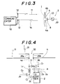
- a voltage is induced in the dipole antenna 4, and hence a reception current I flows.
- the received electric wave ie, the transmission wave 11 emitted from the communicator 10
- the communicator 10 receives the reflected wave 14 by using a reception antenna 13 and demodulates it.
- the impedance between terminals 2b and 2c is changed in accordance with the ON/OFF operation of the FET 8.
- the impedance between the power supply points 4a and 4b becomes a value, for example, 50 ( ⁇ ), at which the dipole antenna 4 is matched with the transmission wave 11 of 2.45 GHz.
- the impedance between the power supply points 4a and 4b becomes, for example, 100 ( ⁇ ), so that mismatching between the wave 11 and the dipole antenna 4 occurs.
- the reflection characteristics of the dipole antenna 4 are changed depending on whether matching is achieved or not.
- the phase or amplitude of the reflected wave 14 when matching is achieved differs from that of the reflected wave 14 when mismatching occurs. That is, the ID tag device phase-modulates or amplitude-modulates a received electric wave, ie, transmission wave 11 from the communicator 10 by ON/OFF operating the FET 8 and supply the modulated wave to the communicator 10 by reflecting it. Subsequently, in the communicator 10, the transmission wave 11 and the reflected wave 14 are compared with each other to perform phase or amplitude demodulation, thereby obtaining data.
- the communicator 10 can detect the identification code ID. Accordingly, a carrier for transmitting the identification code ID to the communicator 10 need not be generated in the ID tag device, and hence a transmitting circuit and a power source for transmission are not required in the ID tag device. In addition, since the reflected wave 14 is automatically generated upon reception of the transmission wave 11 from the communicator 10, a receiving circuit for transmitting the identification code ID in response to the transmission wave 11 from the communicator and a power source for signal reception are not required.
- the ID tag device can be continuously operated for about one year by using a button battery having a small capacity of about 10 mA/h.
- This ID tag device can be used in various fields by changing data to be written in the memory 7. If, for example, personal data is written, the ID tag device can be used in a management system for people passing through a gate.
- the tag 1 is preferably formed into a card-like shape.
- a microstrip antenna may be used.
- FIG. 4 is a circuit diagram showing the main part of a reflecting transmitter according to another embodiment of the present invention.
- a series circuit consisting of a diode D and a capacitor C1 is connected between power supply points 4a and 4b of a dipole antenna 4, and the node of the diode D and the capacitor C1 is connected to a terminal 2a of an identification code generator 2.
- the other terminal (supply power point 4b) of capacitor C1 is connected to a terminal 2b.
- the transmission wave 11 from the communicator 10 received by the dipole antenna 4 is doubled due to the squaring characteristic of the diode D, and a second order harmonic of the transmission wave 11 is re-emitted from the ID tag device as a reflected wave 21.
- a transmission pole antenna 20 which resonates with the second-order harmonic is arranged in the device, and power supply points 20a and 20b are respectively connected to the power supply points 4a and 4b of the dipole antenna 4. With this arrangement, the second-order harmonic can be efficiently re-emitted.
- the transmission wave 11 from the communicator 10 received by the dipole antenna 4 is rectified by the diode D and charges the capacitor C1.
- a voltage is generated across the capacitor C1 as indicated by an arrow A, and this voltage is applied to the identification code generator 2 through the terminals 2a and 2b.
- the voltage generated at the portion indicated by the arrow A varies depending on an electric field intensity at a reception point. In the normal state, the voltage ranges from several mV to several V, and hence can be sufficiently great as to operate the generator 2.
- FIG. 5 is a block diagram showing a data generating circuit 9.
- data is stored in a shift register 22 obtained by connecting a plurality of series-connected flip-flops FF.
- This shift register 22 is designed to serve as a serial-input/output type register so that data consisting of a stream of 0's and 1's is output in units of bits from the last-stage flip-flop FFn and is supplied to the terminal 2c (output terminal) as the identification code ID.
- Outputs from the last-stage flip-flop FFn are input to a first-stage flip-flop FF1 again so as to cyclically generate data.
- the identification code data ID supplied to the terminal 2c is supplied to the anode of the diode D via a capacitor C2 and coil L1.
- the diode D connects or disconnects the power supply points 20a and 20b (4a and 4b) in accordance with the identification code ID, so that the impedance of the transmission dipole antenna 20 is changed in accordance with the identification code ID. Since a state (a phase, an amplitude, and the like) of the reflected wave 21 re-emitted from the transmission antenna 20 is changed in accordance with the identification code ID, the data generated by the data generator 9 can be transmitted receiving and demodulating the reflected wave 21 in the communicator 10.
- the coil L1 is a high-frequency choke coil and serves to prevent the reception wave 11 from flowing to the terminal 2c.
- a shunt capacitor C3 is connected between the node of the capacitor C2 and the coil L1 and the ground so as to ground the data output line to high-frequency signals, thereby preventing the reception wave 11 from flowing to the terminal 2c.
- Figure 6 is a block diagram showing a system capable of discriminating and identifying reflected waves from a plurality of ID tag devices. Since data transmission is performed by utilising a reflected wave of an electric wave transmitted from the communicator as described above, if a plurality of ID tag devices are present within an allowable response range of the communicator, waves reflected from these ID tag devices are simultaneously supplied to the communicator, thus causing radio interference.
- a voltage having a sawtooth waveform is applied to a voltage-controlled oscillator (VCO) 26 so as to generate an FM wave having a gradually changing frequencies of ⁇ 0 + ⁇ 0t, and the generated FM wave is transmitted from a transmission antenna 12.
- VCO voltage-controlled oscillator
- the reception frequency at time t is given as ⁇ 0 + ⁇ 0 (t - ⁇ ).
- the reception transmission waves 29 and 28 are supplied to a mixer 27 so as to obtain an output signal having a frequency difference ⁇ 0.
- ⁇ corresponding to a difference between the waves 28 and 29, and supplies this signal to a frequency demodulator 30. Since the time interval ⁇ required for the wave to be reflected and returned by each ID tag device is changed in accordance with a distance between the communicator 31 and the ID tag device, the frequency difference corresponding to the distance between the communicator 31 and each ID tag device can be obtained. Therefore, even when a plurality of ID tag devices are present, if the distances between the communicator 31 and the respective ID tags are different from each other, simultaneously supplied reflected waves can be separated by utilising the fact that the frequency difference ⁇ o ⁇ varies in each reflected wave.
- an output demodulated from a reflected wave from an ID tag device located at a specific position ( ⁇ is a predetermined value) can be obtained from the demodulator 30 which demodulate a specific frequency.
- this output is, eg, phase-demodulated, data transmitted from the ID tag device can be regenerated.
- the memory 107 has a storage capacity of, eg, several hundreds of bits.
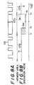
- the first several tens of bits of the memory 107 are used as an exclusive read area (ROM) 107a, in which a frame sync signal 108 used for regeneration of a bit clock shown in figure 8A is written. Accordingly, the area 107a constitutes a sync signal generating circuit.
- ROM exclusive read area
- a user area 107b (RAM) is arranged in a portion other than the read area 107a.
- RAM random access memory
- ground and input/output terminals 123 and 125 arranged in a programmer 122 are respectively brought into contact with the elements of the dipole antenna 104 at the ground and signal input sides so as to read the frame sync signal 108 supplied to the dipole antenna 104.
- the programmer 122 regenerates a bit clock ck in the data generating circuit 102 from the frame sync signal 108, and generates a data write bit block synchronised with the bit clock ck.
- a predetermined code signal SW is output from the input/output terminal 125 as a signal for switching the memory circuit 107 operated in a read mode R to a write mode W at time t1 immediately after the frame sync signal 108 is transmitted, as shown in a timing chart of figure 8B.
- This code signal SW may be a bit clock having a predetermined frequency.
- the code signal SW input from the dipole antenna 104 to the data generating circuit 102 is supplied to one input terminal of a coincidence detecting circuit 110 and the memory 107 through a buffer amplifier 111.
- the coincidence detecting circuit 110 comprises an exclusive OR gate.
- the bit clock ck is supplied from the oscillator 105 to the other input terminal of coincidence detecting circuit 110.
- a coincidence detection signal is supplied to the set terminal S of a flip-flop circuit 112.
- the flip-flop circuit 112 is set, and the level of a control signal output from the output terminal Q thereof is inverted, so that the memory 107 is switched from the read mode R t the write mode W at time t2 in figure 8B.
- this control signal is supplied to the gate circuit 113 through an inverter 115, so that the gate circuit 113 is turned off when the memory 107 is set in the write mode. As a result, the FET 114 is turned off.
- the data generating circuit 102 is operated in the write mode W in this manner. Therefore, if arbitrary data of, eg, the type of goods, a receipt number, a receipt data and a destination are transmitted from the programmer 122 upon transmission of the code signal SW, these data are sequentially written in the user area 107b.
- the address designation count of the address counter 106 is returned to an initial value.
- a reset signal is output from the control output terminal Q of the address counter 106 to the reset terminal R of the flip-flop circuit 112 as a signal Search report for switching the memory circuit 107 to the read mode R. Since the flip-flop circuit 112 is reset, and the level of a control signal output from the output terminal Q is inverted, the memory 107 is switched to the read mode R at time t3 in figure 8B and the gate circuit 113 is turned on.
- the data written in the user area 107b is read following the frame sync signal 108 written in the read area 107a.
- the read data is supplied to the gate electrode of the FET 114 as an identification code ID, and is transmitted from the dipole antenna 104.
- FIG. 9 is a block diagram showing a data transmitter according to still another embodiment of the present invention.
- an independent input terminal 102d is arranged in a data generating circuit 102, and an external input terminal 126 is arranged at an end portion of a tag 101, as shown in the plan view of an ID tag device of figure 10.
- These terminals 102d and 126 are connected to each other.
- a frame sync signal 108 transmitted from a dipole antenna 104 is received by a reception antenna 124 mounted on a programmer 122 so as to regenerate a bit clock, and a data write bit clock of the programmer 122 is generated.
- a write terminal 122a of the programmer 122 is brought into contact with the external input terminal 126 of the ID tag device.
- this contact operation is performed such that an insertion hole is formed in the programmer 122, and the ID tag device is inserted into this insertion hole, thereby bringing the terminals 102d and 126 into contact with each other.
- This embodiment further comprises a pattern generator 130 for generating a code signal having a predetermined bit pattern on the basis of a clock output from a clock signal generator 105.
- a code signal generated by this generator 130 is supplied to the other input terminal of the coincidence detecting circuit 110 as a comparison reference signal. Therefore, when the memory 107 is to be switched to the write mode, a code signal having the same pattern as that of the code signal generated by the generator 130 is supplied from the programmer 122 as a switching signal SW for switching the memory 107 to the write mode.
- a predetermined code signal SW can be input while the frame sync signal 108 is read. Therefore, the memory 107 is switched to the write mode W at time t1 when transmission of the frame sync signal 108 is completed.
- a signal having the same bit pattern as that of the frame sync signal 108 can be used as the predetermined code signal.
- the comparison reference signal having this bit pattern may be generated by the pattern generator 130, or a signal written in the area 107a of the memory 107 may be used as the comparison reference signal.
- a sync signal circuit may be designed so as to cause the pattern generator 130 to generate a bit pattern for a frame sync signal and periodically output it from the antenna 104.
- the frame sync signal 108 need not be written in the memory 107 in advance.
- a signal Search report for switching the memory circuit 107 to the read mode can be externally input upon completion of a write operation.
- the impedance of the antenna is changed by transmission data so as to change the reflection characteristics of the antenna so that the transmission data can be carried by a reflected wave. Therefore, a transmitting circuit which generates a carrier for transmitting data and a transmission power source are not required. Consequently, a small, low-cost data transmitter which is operated by a very low power can be manufactured with a simple circuit arrangement.
- bit-synchronised data can be formed on the write data source side on the basis of the sync signal. Consequently, an exclusive output terminal for bit clock need nt be arranged in the transmitter.
- terminals required for writing of transmission data in the memory can be eliminated, and a highly reliable low-cost data write type transmitter can be obtained.
Landscapes
- Engineering & Computer Science (AREA)
- Physics & Mathematics (AREA)
- Remote Sensing (AREA)
- Radar, Positioning & Navigation (AREA)
- General Physics & Mathematics (AREA)
- Computer Networks & Wireless Communication (AREA)
- Automation & Control Theory (AREA)
- Electromagnetism (AREA)
- Computer Security & Cryptography (AREA)
- Computer Hardware Design (AREA)
- Microelectronics & Electronic Packaging (AREA)
- Theoretical Computer Science (AREA)
- Mechanical Engineering (AREA)
- Acoustics & Sound (AREA)
- Radar Systems Or Details Thereof (AREA)
- Near-Field Transmission Systems (AREA)
- Transmitters (AREA)
Applications Claiming Priority (4)
| Application Number | Priority Date | Filing Date | Title |
|---|---|---|---|
| JP63006292A JP2705076B2 (ja) | 1988-01-14 | 1988-01-14 | 反射型送信装置 |
| JP6292/88 | 1988-01-14 | ||
| JP9993/88 | 1988-01-20 | ||
| JP63009993A JP2595606B2 (ja) | 1988-01-20 | 1988-01-20 | データ送信装置 |
Publications (3)
| Publication Number | Publication Date |
|---|---|
| EP0324564A2 true EP0324564A2 (fr) | 1989-07-19 |
| EP0324564A3 EP0324564A3 (fr) | 1991-05-15 |
| EP0324564B1 EP0324564B1 (fr) | 1995-07-12 |
Family
ID=26340389
Family Applications (1)
| Application Number | Title | Priority Date | Filing Date |
|---|---|---|---|
| EP89300147A Expired - Lifetime EP0324564B1 (fr) | 1988-01-14 | 1989-01-09 | Système pour transmettre des informations d'identité et des données analogues |
Country Status (6)
| Country | Link |
|---|---|
| EP (1) | EP0324564B1 (fr) |
| KR (1) | KR0142673B1 (fr) |
| AU (1) | AU625452B2 (fr) |
| CA (1) | CA1335676C (fr) |
| DE (1) | DE68923383T2 (fr) |
| MY (1) | MY104725A (fr) |
Cited By (18)
| Publication number | Priority date | Publication date | Assignee | Title |
|---|---|---|---|---|
| WO1992017866A1 (fr) * | 1991-04-03 | 1992-10-15 | Integrated Silicon Design Pty. Ltd. | Systeme de tri d'articles |
| WO1993020459A1 (fr) * | 1992-04-03 | 1993-10-14 | Tommy Olsson | Procede et appareil de marquage anti-vol destine a des equipements de bureau, tels que des ordinateurs notamment |
| EP0693695A1 (fr) * | 1993-05-21 | 1996-01-24 | Texas Instruments Deutschland Gmbh | Système d'identification bi-standard à fréquence radio |
| WO1996007938A1 (fr) * | 1994-09-09 | 1996-03-14 | International Business Machines Corporation | Etiquette d'identification radiofrequence |
| FR2730557A1 (fr) * | 1995-02-10 | 1996-08-14 | Giat Ind Sa | Mine d'exercice, dispositif de programmation et dispositif de simulation mettant en oeuvre une telle mine |
| FR2738968A1 (fr) * | 1995-09-19 | 1997-03-21 | Thomson Csf | Procede de localisation d'un emetteur-recepteur de paquets de donnees et emetteur-recepteur mettant en oeuvre ce procede |
| EP0779520A3 (fr) * | 1995-12-12 | 1997-09-17 | ||
| WO1998001837A1 (fr) * | 1996-07-05 | 1998-01-15 | Integrated Silicon Design Pty. Ltd. | Etiquette de donnes et presence |
| WO1998027440A1 (fr) * | 1996-12-16 | 1998-06-25 | Siemens Aktiengesellschaft | Transpondeur comportant une antenne de reception a hyperfrequences |
| EP0435137B1 (fr) * | 1989-12-19 | 1999-07-28 | Sony Corporation | Système de carte d'information |
| WO2001001649A1 (fr) * | 1999-06-25 | 2001-01-04 | Marconi Data Systems Ltd. | Circuit modulateur de reflexion comprenant un amplificateur a impedance negative |
| US6243012B1 (en) | 1996-12-31 | 2001-06-05 | Lucent Technologies Inc. | Inexpensive modulated backscatter reflector |
| GB2367174A (en) * | 2000-09-25 | 2002-03-27 | Gadget Guard Ltd | A method and apparatus for security tagging |
| EP1211635A3 (fr) * | 2000-11-30 | 2002-08-14 | Supersensor (Proprietary) Limited | Agencement d'impédance d'entrée pour transpondeur RF |
| EP1110191A4 (fr) * | 1998-09-11 | 2005-02-02 | Motorola Inc | Circuit optimise pour badge hf electrostatique et procede correspondant |
| US6941278B2 (en) * | 1998-04-08 | 2005-09-06 | Hitachi, Ltd. | Freight information management method and freight management system using electronic tags |
| US7598864B2 (en) | 2003-12-03 | 2009-10-06 | Fec Co., Ltd. | IC chip for identification, method for reading out data therefrom, and method for writing data thereinto |
| US9618366B2 (en) | 2014-11-25 | 2017-04-11 | Mitutoyo Corporation | Absolute encoder scale configuration with unique coded impedance modulations |
Families Citing this family (16)
| Publication number | Priority date | Publication date | Assignee | Title |
|---|---|---|---|---|
| JPH03113387A (ja) * | 1989-09-27 | 1991-05-14 | Nippon Soken Inc | 移動体識別装置の応答器 |
| US5030807A (en) * | 1990-01-16 | 1991-07-09 | Amtech Corporation | System for reading and writing data from and into remote tags |
| GB9013349D0 (en) * | 1990-06-14 | 1990-10-17 | Marconi Gec Ltd | Transponder system |
| DE4102816C2 (de) * | 1990-07-27 | 1994-06-30 | Diehl Gmbh & Co | Hochfrequenz-Kommunikationseinrichtung |
| US5030940A (en) * | 1990-08-02 | 1991-07-09 | Sensormatic Electronics Corporation | Electronic article surveillance tag and method for implementing same |
| JPH0496520A (ja) * | 1990-08-13 | 1992-03-27 | Sharp Corp | データ送信装置 |
| US5247305A (en) * | 1990-10-10 | 1993-09-21 | Nippondenso Co., Ltd. | Responder in movable-object identification system |
| KR100227055B1 (ko) * | 1990-11-06 | 1999-10-15 | 로데릭 더블류 루이스 | 이중 모드 전자 식별 시스템 및 태그 |
| FR2669484B1 (fr) * | 1990-11-16 | 1994-03-25 | Thomson Composants Microondes | Dispositif de telecommunications par ondes electromagnetiques. |
| FR2674055A1 (fr) * | 1991-03-14 | 1992-09-18 | Bertin Jean Claude | Dispositif pour l'authentification d'un produit. |
| JPH07174845A (ja) * | 1993-12-17 | 1995-07-14 | Omron Corp | 符号応答方法およびその方法を実施するための符号応答器並びにその符号応答器が用いられた符号応答システム |
| US5729197A (en) * | 1996-02-22 | 1998-03-17 | Ultra Communications Corporation | Automatic, self-triggering alarm processing system and method |
| AU710635B2 (en) * | 1996-07-05 | 1999-09-23 | Gemplus | Presence and data labels |
| US5883592A (en) * | 1997-12-10 | 1999-03-16 | Sarnoff Corporation Secom | Method and apparatus for remotely identifying an electronically coded article |
| US6107920A (en) * | 1998-06-09 | 2000-08-22 | Motorola, Inc. | Radio frequency identification tag having an article integrated antenna |
| JP2001345638A (ja) * | 2000-06-01 | 2001-12-14 | Alps Electric Co Ltd | 3バンド切替型発振器 |
Family Cites Families (10)
| Publication number | Priority date | Publication date | Assignee | Title |
|---|---|---|---|---|
| US3631484A (en) * | 1969-07-30 | 1971-12-28 | Microlab Fxr | Harmonic detection system |
| AU1250170A (en) * | 1970-03-12 | 1971-09-16 | Unisearch Limited | Electronic surveillance system |
| US3895368A (en) * | 1972-08-09 | 1975-07-15 | Sensormatic Electronics Corp | Surveillance system and method utilizing both electrostatic and electromagnetic fields |
| US4075632A (en) * | 1974-08-27 | 1978-02-21 | The United States Of America As Represented By The United States Department Of Energy | Interrogation, and detection system |
| GB1567750A (en) * | 1975-09-19 | 1980-05-21 | Seldown Electronics Ltd | Transponders |
| US4242663A (en) * | 1979-02-01 | 1980-12-30 | Lockheed Electronics Corporation | Electronic identification system |
| EP0170716B1 (fr) * | 1984-08-08 | 1990-10-24 | Kabushiki Kaisha Toshiba | Porteur d'information |
| US4656472A (en) * | 1985-01-23 | 1987-04-07 | Walton Charles A | Proximity identification system with power aided identifier |
| US4786907A (en) * | 1986-07-14 | 1988-11-22 | Amtech Corporation | Transponder useful in a system for identifying objects |
| GB2202415A (en) * | 1987-03-17 | 1988-09-21 | Ferranti Plc | Object identification system |
-
1989
- 1989-01-04 CA CA000587475A patent/CA1335676C/fr not_active Expired - Lifetime
- 1989-01-05 AU AU27750/89A patent/AU625452B2/en not_active Expired
- 1989-01-07 MY MYPI89000004A patent/MY104725A/en unknown
- 1989-01-09 DE DE68923383T patent/DE68923383T2/de not_active Expired - Lifetime
- 1989-01-09 EP EP89300147A patent/EP0324564B1/fr not_active Expired - Lifetime
- 1989-01-11 KR KR1019890000218A patent/KR0142673B1/ko not_active Expired - Lifetime
Cited By (26)
| Publication number | Priority date | Publication date | Assignee | Title |
|---|---|---|---|---|
| EP0435137B1 (fr) * | 1989-12-19 | 1999-07-28 | Sony Corporation | Système de carte d'information |
| WO1992017866A1 (fr) * | 1991-04-03 | 1992-10-15 | Integrated Silicon Design Pty. Ltd. | Systeme de tri d'articles |
| WO1993020459A1 (fr) * | 1992-04-03 | 1993-10-14 | Tommy Olsson | Procede et appareil de marquage anti-vol destine a des equipements de bureau, tels que des ordinateurs notamment |
| EP0693695A1 (fr) * | 1993-05-21 | 1996-01-24 | Texas Instruments Deutschland Gmbh | Système d'identification bi-standard à fréquence radio |
| WO1996007938A1 (fr) * | 1994-09-09 | 1996-03-14 | International Business Machines Corporation | Etiquette d'identification radiofrequence |
| US5801322A (en) * | 1995-02-10 | 1998-09-01 | Giat Industries | Exercise mine and programming and simulation device therefor |
| FR2730557A1 (fr) * | 1995-02-10 | 1996-08-14 | Giat Ind Sa | Mine d'exercice, dispositif de programmation et dispositif de simulation mettant en oeuvre une telle mine |
| WO1996024818A1 (fr) * | 1995-02-10 | 1996-08-15 | Giat Industries | Mine d'exercice, dispositif de programmation et dispositif de simulation mettant en ×uvre une telle mine |
| FR2738968A1 (fr) * | 1995-09-19 | 1997-03-21 | Thomson Csf | Procede de localisation d'un emetteur-recepteur de paquets de donnees et emetteur-recepteur mettant en oeuvre ce procede |
| EP0764854A1 (fr) * | 1995-09-19 | 1997-03-26 | Thomson-Csf | Procédé de localisation d'un émetteur-récepteur de paquets de données et émetteur-récepteur mettant en oeuvre ce procédé |
| EP0779520A3 (fr) * | 1995-12-12 | 1997-09-17 | ||
| WO1998001837A1 (fr) * | 1996-07-05 | 1998-01-15 | Integrated Silicon Design Pty. Ltd. | Etiquette de donnes et presence |
| WO1998027440A1 (fr) * | 1996-12-16 | 1998-06-25 | Siemens Aktiengesellschaft | Transpondeur comportant une antenne de reception a hyperfrequences |
| US6243012B1 (en) | 1996-12-31 | 2001-06-05 | Lucent Technologies Inc. | Inexpensive modulated backscatter reflector |
| US6941278B2 (en) * | 1998-04-08 | 2005-09-06 | Hitachi, Ltd. | Freight information management method and freight management system using electronic tags |
| EP1110191A4 (fr) * | 1998-09-11 | 2005-02-02 | Motorola Inc | Circuit optimise pour badge hf electrostatique et procede correspondant |
| US7046957B1 (en) | 1999-06-25 | 2006-05-16 | Adrian N Farr | Reflecting modulator circuit comprising a negative impedance amplifier |
| WO2001001649A1 (fr) * | 1999-06-25 | 2001-01-04 | Marconi Data Systems Ltd. | Circuit modulateur de reflexion comprenant un amplificateur a impedance negative |
| US7551903B2 (en) | 1999-06-25 | 2009-06-23 | Adrian N Farr | Reflecting modulator circuit comprising a negative impedance amplifier |
| GB2367174B (en) * | 2000-09-25 | 2002-08-07 | Gadget Guard Ltd | A method and apparatus for security tagging |
| GB2367174A (en) * | 2000-09-25 | 2002-03-27 | Gadget Guard Ltd | A method and apparatus for security tagging |
| EP1211635A3 (fr) * | 2000-11-30 | 2002-08-14 | Supersensor (Proprietary) Limited | Agencement d'impédance d'entrée pour transpondeur RF |
| US6870460B2 (en) | 2000-11-30 | 2005-03-22 | Supersensor (Proprietary) Limited | Input impedance arrangement for RF transponder |
| EP1760639A1 (fr) * | 2000-11-30 | 2007-03-07 | ZIH Corporation | Agencement d'impédance d'entrée pour transpondeur RF |
| US7598864B2 (en) | 2003-12-03 | 2009-10-06 | Fec Co., Ltd. | IC chip for identification, method for reading out data therefrom, and method for writing data thereinto |
| US9618366B2 (en) | 2014-11-25 | 2017-04-11 | Mitutoyo Corporation | Absolute encoder scale configuration with unique coded impedance modulations |
Also Published As
| Publication number | Publication date |
|---|---|
| EP0324564B1 (fr) | 1995-07-12 |
| EP0324564A3 (fr) | 1991-05-15 |
| DE68923383T2 (de) | 1995-11-30 |
| KR890012458A (ko) | 1989-08-26 |
| MY104725A (en) | 1994-05-31 |
| CA1335676C (fr) | 1995-05-23 |
| DE68923383D1 (de) | 1995-08-17 |
| AU2775089A (en) | 1989-07-20 |
| KR0142673B1 (ko) | 1998-08-17 |
| AU625452B2 (en) | 1992-07-09 |
Similar Documents
| Publication | Publication Date | Title |
|---|---|---|
| EP0324564B1 (fr) | Système pour transmettre des informations d'identité et des données analogues | |
| KR100321434B1 (ko) | 정보카드장치 | |
| US5606323A (en) | Diode modulator for radio frequency transponder | |
| US6243013B1 (en) | Cascaded DC voltages of multiple antenna RF tag front-end circuits | |
| US5966082A (en) | Method of flagging partial write in RF tags | |
| JP2705076B2 (ja) | 反射型送信装置 | |
| US5467082A (en) | Proximity actuator and reader for an electronic access system | |
| US5625341A (en) | Multi-bit EAS marker powered by interrogation signal in the eight MHz band | |
| US5426667A (en) | System for the contactless exchange of data, and responder for use in such a system | |
| EP0390822B1 (fr) | Appareil et procede d'identification | |
| US4242663A (en) | Electronic identification system | |
| US7348875B2 (en) | Semi-passive radio frequency identification (RFID) tag with active beacon | |
| US7321290B2 (en) | Radio tag and system | |
| EP0254954B1 (fr) | Répondeur dans un système d'identification | |
| US5485154A (en) | Communication device and method(s) | |
| EP1251452A1 (fr) | Etiquette d'identification électronique multimémoire | |
| US6731199B1 (en) | Non-contact communication system | |
| CA2058330C (fr) | Systeme et methode de transmission de donnees sans contact | |
| RU2137161C1 (ru) | Носитель данных для идентификации объектов и способ управления им | |
| JP3568714B2 (ja) | 非接触通信システム及びそれに使用する質問器 | |
| US4857913A (en) | Coded objects identifiable by proximity and devices for changing the codes of these objects | |
| JP2840832B2 (ja) | 反射型送信装置 | |
| JP2682233B2 (ja) | 移動体識別装置 | |
| EP0641450A4 (fr) | Systeme electronique et procede permettant l'identification a distance d'articles codes et analogue. | |
| JP2705076C (fr) |
Legal Events
| Date | Code | Title | Description |
|---|---|---|---|
| PUAI | Public reference made under article 153(3) epc to a published international application that has entered the european phase |
Free format text: ORIGINAL CODE: 0009012 |
|
| AK | Designated contracting states |
Kind code of ref document: A2 Designated state(s): DE FR GB NL |
|
| PUAL | Search report despatched |
Free format text: ORIGINAL CODE: 0009013 |
|
| RHK1 | Main classification (correction) |
Ipc: G01S 13/02 |
|
| AK | Designated contracting states |
Kind code of ref document: A3 Designated state(s): DE FR GB NL |
|
| 17P | Request for examination filed |
Effective date: 19910903 |
|
| 17Q | First examination report despatched |
Effective date: 19930830 |
|
| GRAA | (expected) grant |
Free format text: ORIGINAL CODE: 0009210 |
|
| AK | Designated contracting states |
Kind code of ref document: B1 Designated state(s): DE FR GB NL |
|
| REF | Corresponds to: |
Ref document number: 68923383 Country of ref document: DE Date of ref document: 19950817 |
|
| ET | Fr: translation filed | ||
| PLBE | No opposition filed within time limit |
Free format text: ORIGINAL CODE: 0009261 |
|
| STAA | Information on the status of an ep patent application or granted ep patent |
Free format text: STATUS: NO OPPOSITION FILED WITHIN TIME LIMIT |
|
| 26N | No opposition filed | ||
| REG | Reference to a national code |
Ref country code: GB Ref legal event code: IF02 |
|
| PGFP | Annual fee paid to national office [announced via postgrant information from national office to epo] |
Ref country code: DE Payment date: 20080104 Year of fee payment: 20 Ref country code: NL Payment date: 20080103 Year of fee payment: 20 Ref country code: GB Payment date: 20080109 Year of fee payment: 20 |
|
| PGFP | Annual fee paid to national office [announced via postgrant information from national office to epo] |
Ref country code: FR Payment date: 20080108 Year of fee payment: 20 |
|
| REG | Reference to a national code |
Ref country code: GB Ref legal event code: PE20 Expiry date: 20090108 |
|
| NLV7 | Nl: ceased due to reaching the maximum lifetime of a patent |
Effective date: 20090109 |
|
| PG25 | Lapsed in a contracting state [announced via postgrant information from national office to epo] |
Ref country code: NL Free format text: LAPSE BECAUSE OF EXPIRATION OF PROTECTION Effective date: 20090109 |
|
| PG25 | Lapsed in a contracting state [announced via postgrant information from national office to epo] |
Ref country code: GB Free format text: LAPSE BECAUSE OF EXPIRATION OF PROTECTION Effective date: 20090108 |