EP0324855A1 - Procede et dispositif de detection aux ultrasons de defectuosites - Google Patents
Procede et dispositif de detection aux ultrasons de defectuosites Download PDFInfo
- Publication number
- EP0324855A1 EP0324855A1 EP87905793A EP87905793A EP0324855A1 EP 0324855 A1 EP0324855 A1 EP 0324855A1 EP 87905793 A EP87905793 A EP 87905793A EP 87905793 A EP87905793 A EP 87905793A EP 0324855 A1 EP0324855 A1 EP 0324855A1
- Authority
- EP
- European Patent Office
- Prior art keywords
- pulse
- gate
- circuit
- delay
- delayed
- Prior art date
- Legal status (The legal status is an assumption and is not a legal conclusion. Google has not performed a legal analysis and makes no representation as to the accuracy of the status listed.)
- Withdrawn
Links
- 238000001514 detection method Methods 0.000 title claims abstract description 43
- 238000000034 method Methods 0.000 title claims description 25
- 230000003111 delayed effect Effects 0.000 claims description 49
- 239000000523 sample Substances 0.000 claims description 6
- 238000002604 ultrasonography Methods 0.000 claims description 6
- 239000007788 liquid Substances 0.000 claims description 3
- 230000001960 triggered effect Effects 0.000 claims 3
- 230000000630 rising effect Effects 0.000 abstract 1
- 238000010586 diagram Methods 0.000 description 17
- 238000002592 echocardiography Methods 0.000 description 10
- 239000000463 material Substances 0.000 description 8
- 230000008569 process Effects 0.000 description 6
- 229910000831 Steel Inorganic materials 0.000 description 5
- 239000010959 steel Substances 0.000 description 5
- 238000007796 conventional method Methods 0.000 description 4
- XLYOFNOQVPJJNP-UHFFFAOYSA-N water Substances O XLYOFNOQVPJJNP-UHFFFAOYSA-N 0.000 description 4
- 230000008859 change Effects 0.000 description 3
- 230000009467 reduction Effects 0.000 description 2
- 239000003990 capacitor Substances 0.000 description 1
- 239000000919 ceramic Substances 0.000 description 1
- 230000003247 decreasing effect Effects 0.000 description 1
- 230000001934 delay Effects 0.000 description 1
- 230000000694 effects Effects 0.000 description 1
- 239000011521 glass Substances 0.000 description 1
- PCHJSUWPFVWCPO-UHFFFAOYSA-N gold Chemical compound [Au] PCHJSUWPFVWCPO-UHFFFAOYSA-N 0.000 description 1
- 239000010931 gold Substances 0.000 description 1
- 229910052737 gold Inorganic materials 0.000 description 1
- 239000012770 industrial material Substances 0.000 description 1
- 239000007769 metal material Substances 0.000 description 1
- 230000000644 propagated effect Effects 0.000 description 1
Images







Classifications
-
- G—PHYSICS
- G01—MEASURING; TESTING
- G01N—INVESTIGATING OR ANALYSING MATERIALS BY DETERMINING THEIR CHEMICAL OR PHYSICAL PROPERTIES
- G01N29/00—Investigating or analysing materials by the use of ultrasonic, sonic or infrasonic waves; Visualisation of the interior of objects by transmitting ultrasonic or sonic waves through the object
- G01N29/04—Analysing solids
-
- G—PHYSICS
- G01—MEASURING; TESTING
- G01N—INVESTIGATING OR ANALYSING MATERIALS BY DETERMINING THEIR CHEMICAL OR PHYSICAL PROPERTIES
- G01N29/00—Investigating or analysing materials by the use of ultrasonic, sonic or infrasonic waves; Visualisation of the interior of objects by transmitting ultrasonic or sonic waves through the object
- G01N29/36—Detecting the response signal, e.g. electronic circuits specially adapted therefor
- G01N29/38—Detecting the response signal, e.g. electronic circuits specially adapted therefor by time filtering, e.g. using time gates
Definitions
- the present invention relates to an ultrasonic method and apparatus for detecting internal flaws possibly existent in materials and products, and more particularly to an ultrasonic method and apparatus suitably usable for inspecting an object for any flaw possibly included in the object and near the surface of thereof and plural fine flaws possibly included in the proximity of each other in the direction of the thickness of the object.
- the objects to which the present invention is applicable include materials and products, such as metallic materials, nonmetallic materials like ceramics, glass, etc., and electronic parts such as ICs and LSIs through which the ultrasound can be propagated.
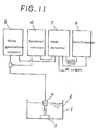
- Fig. 11 is an explanatory drawing of an ultrasonic flaw detector.
- the reference numeral 1 indicates a water bath filled with water 2
- 3 indicates an thin material as object placed on the bottom of the water bath 1
- 4 indicates a probe immersed in water 2.
- the reference numeral indicates a pulse generation circuit which produces ultrasound pulses
- 6 indicates a receiver circuit to receive and amplify the reflected ultrasound wave from the surface of the object 3, flaw therein and the bottom thereof through the probe 4
- 7 indicates a peak detector which detects the peak value of the reflected ultrasound wave amplified by the receiver circuit 6 and provides as a flaw information a DC voltage proportional to the peak value
- 8 indicates a processor which receives and processes a signal delivered from the peak detector 7.
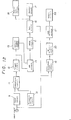
- Fig. 12 is a schematic block diagram of the above-mentioned peak detector 7, and Fig. 12 shows, by way of example, the detail of the essential portion of the peak detector 7.
- the reference numeral 9 indicates an input circuit to which an RF signal of the reflected ultrasound wave amplified by the aforementioned receiver circuit 6 is supplied
- 10 indicates a threshold setting circuit to set a threshold of signal level
- 11 indicates a comparison circuit in which an output signal from the input circuit 9 is compared with a threshold set by the threshold setting circuit
- 12 indicates a trigger circuit which generates a trigger signal to provide a trigger when the output signal from the input circuit 9 compared with the threshold in the comparison circuit 11 exceeds the threshold
- 13 indicates a delayed trigger circuit which is tripped by the trigger signal from the trigger circuit 12, when the level of the transmitted pulse T from the aforementioned probe 5 exceeds the threshold, and sets the width of a delayed trigger pulse
- 14 indicates an AND circuit which receives three signals, that is, the trigger signal from the trigger circuit 12, pulse signal from the delayed trigger circuit 13 and a signal derived from the passage of the pulse signal through a flip-flop and produces a pulse resulted from ANDing of'these three signals
- 15 indicates a delay circuit which
- the reference numeral 19 indicates a detection input circuit which matches the RF signal of the reflected wave amplified by the aforementioned receiver circuit 6 and the output pulse from the gate circuit 16, 20 indicates an RF detection circuit which detects the RF signal from the detection input circuit 19, 21 indicates a peak detection circuit which converts the output signal from the RF detection circuit 20 to a DC voltage proportional to the value of the output signal and maintains the value until the gate pulse from the gate circuit 16 turns off, and 22 indicates an output circuit which delivers the above-mentioned DC voltage as an flaw information.
- Fig. 14 is a characteristic diagram of the pulses obtained when an object is inspected by the aforementioned flaw detector.
- (a) indicates an example echo pattern of the reflected wave from the object 3
- T indicates a transmitted pulse
- S indicates a surface echo
- F indicates a flaw echo
- B indicates a bottom echo
- L indicates a line indicative of a threshold for the levels of the transmitted pulse T and'each echoes.
- (b) indicates a delayed trigger pulse having a width P t set by the delayed trigger circuit 13
- (c) indicates an output pulse delivered from the AND circuit 14, which rises when the surface echo S exceeds the threshold L
- (d) indicate a delayed pulse having a width P d set by the delay circuit 15
- (e) indicates a gate pulse having a width P g set by the gate circuit 16.
- the pulse characteristic diagram shown in Fig. 14 is obtained from the following actions: Namely, when the level of the pulse T transmitted from the probe 4 exceeds the threshold L, the delayed trigger circuit 13 is tripped by the trigger signal from the trigger circuit 12 and the width P t of the delayed trigger pulse is set. Next, when the level of the surface echo S exceeds the threshold L, the AND circuit is tripped, then the delay circuit 15 and gate circuit 15 are tripped. Thus a sequence of flaw detecting operations begins. When the width P g of the delayed pulse ends, the gate is opened nearly simultaneously. The gate is closed after the pulse width P g ends. In this case, for the gate pulses to be produced always following up with the surface echo during a flaw detection, the period of time during which the delayed trigger pulse is on is controlled so that the operation sequences of the delay and gate circuits will not be started.
- the aforementioned delayed trigger circuit 13, delay circuit 15 and gate circuit 16 have a one-shot multivibrators 13a, 15a and 16a, respectively. These multivibrators 13a, 15a and 16a work as delayed a time t PLH for pulse propagation from input of a pulse to them until they deliver their output signals. More particularly, the delayed pulse (d) in Fig. 14 does not rise when the level of the surface echo S has exceeded the threshold L but rises as delayed the time for pulse propagation tp LH in practice. Similarly, the gate pulse (e) shown in Fig. 14 does not turn on at the same time as the fall of the delayed pulse but turns on as delayed the pulse propagation time t PLH in practice.
- this propagation delay time t PLH depends upon the circuit configuration of the multivibrator, but it is said to be nearly 20 to 70 ns. Generally, it is about 30 ns at a temperature of 20°C.
- the minimum values of the pulse width P d and P g settable by the delay circuit 15 and gate circuit 16, respectively, having each a multivibrator are limited to about 60 to 80 ns at present in view of the circuit capacity. Thus, it will take at least a time of (2t PLH + P g ) - 120 to 140 ns from when the level of the surface echo S has exceeded the threshold L until the gate pulse (e) in Fig.
- This time length corresponds to a pulse propagation distance of about 350 to 400 ⁇ m in case of the object made of a steel, for example while it corresponds to a pulse propagation distance of about 200 to 230 ⁇ m in case of the object made of gold.
- the minimum pulse width P d and Pg settable as in the above are about 60 to 80 ns, respectively. Therefore, the pulse propagation distance corresponding to this pulse width is about 200 pm in a steel.
- a flaw existent at a depth of more than about 350 ⁇ m from the surface of the object (more than 200 ⁇ m even when the aforementioned propagation delay time t PLH is not taken in account) can be detected.
- a surface flaw included in the object and at a depth smaller than the above as well as a flaw included in an extremely thin object of less than about 350 ⁇ m in thickness cannot be detected.
- the gate pulse can be set to a selected point and width by the above-mentioned gate circuit 16 and thus it is not possible to develop only the flaw echo F within the width P g of the gate pulse. Also any fine flaws included in the object and beneath the object surface in the direction of the thickness cannot be detected.
- the flaws cannot be detected for the same reason as in the above unless they are spaced more than 350 ⁇ m from each other (more than 200 ⁇ m in case the propagation delay time t PLH is not taken in account) since the flaws cannot be gated separately.
- the conventional ultrasonic method and apparatus for flaw detection do not permit to detect a surface flaw or internal flaw in an extremely thin object as the case may be though it is really existent. Also, internal fine flaws existent near each other in an object in the direction-of the thickness thereof cannot be detected separately in many cases.
- the present invention has a primary object to overcome the above-mentioned drawbacks of the conventional techniques by providing an ultrasonic method and apparatus for flaw detection which permit to positively detect any surface flaw and internal fine flaws in an extremely materials and products.
- an ultrasonic method and apparatus for flaw detection can be provided which can detect plural fine flaws included in an object and near each other in the direction of the thickness of thereof as freely separated.
- a flaw detection is done using a gate pulse obtained through the steps of generating a trigger signal to provide a trigger when the level of a surface echo from an object under flaw detection immersed in a liquid has exceeded a preset threshold, generating a first pulse as delayed, by a first delay line, a predetermined time from the point where the trigger signal has been generated, turning on a gate pulse, with which a flaw echo is inspected, with the rise of the first pulse and simultaneously generating a second pulse as delayed, by a second delay line, a predetermined time from the rise point of the first pulse, and turning off the gate pulse simultaneously with the generation of the second pulse to provide a gate pulse with which the flaw detection is done.
- the above-mentioned flaw detection according to the present invention utilizes the relation between two sets of delay lines provided in the peak detector, which will be described below. Namely, sequential use of two sets of delay lines which can delay the points of pulse generation a predetermined time as desired permits, via the first set of delay lines, to turn on the gate pulse with which the flaw echo is inspected at the rise point of the first pulse generated as delayed the predetermined time from the point where the trigger signal has been generated when the level of the surface echo from the object has exceeded the threshold and at the same time, via the second set of delay lines, to turn off the above-mentioned gate pulse at the point where the second pulse has been generated as delayed the predetermined time from the rise point of the above-mentioned first pulse, whereby the time between the on and off points of the gate pulse, that is, the width of the gate pulse, can be made equal to the aforementioned predetermined delay time due to the second set of delay lines and at the same time the width of the gate pulse be made to coincide with the width of a flaw echo
- the time lengths of delay due to the first and second sets of delay lines vary depending upon the nature of the object under flaw detection (such as material, dimensions, shape, etc.), flaw depth from the surface of the object which is to be inspected, flaw detecting conditions such as probe frequency used and the like, and they vary from one object to another as the case may be even if they are nearly identical to each other in nature, flaw depth to be inspected and the similar respects as in case of ICs. Since so designed as to have the delay time changed stepwisely, the delay line can work within a permissible range. Thus, both the first and second delay lines may be a single line, respectively.
- plural lines used for the first delay line are sequentially delayed up to a predetermined delay time and such stepwise delays are summed up to be the predetermined delay time, as the case may be.
- plural lines are used also for the second delay line as in case of the first delay line, as the case may.
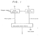
- Fig. 1 is an explanatory drawing showing the correlation between the two sets of delay lines
- Fig. 2 is a characteristic diagram derived from the correlation shown in Fig. 1.
- the first pulse is delivered to a second delay line 32 and also to a gate pulse output device 33.
- a second pulse (e) as shown in Fig. 2 by delaying the first pulse a predetermined time t d2 from the point where the first pulse has been generated.
- the second pulse is delivered to the gate pulse output device 33.
- This gate pulse output device 33 consists of a logic circuit and inverter in which the first and second pulses are logically processed to provide a gate pulse (f) as shown in Fig. 2 which has a width P G corresponding to the width of the flaw echo F.
- the width PG of the gate pulse (f) is equal to the delay time t d2 due to the second delay line 32.
- the reduction of the delay time t d2 leads to reduction of the gate pulse width P G .
- the predetermined'delay time t dl and t d2 set by the first and second delay lines 31 and 32, respectively, vary depending upon the flaw detecting conditions and the kind of object under flaw detection as having been described in the foregoing.
- the first and second delay lines 31 and 32 have their delay time t d1 and t d2 changeable stepwisely, a desired delay time can be freely selected by selecting a kind of the delay line, the points where the first and second pulses are generated can be set freely and easily, and also the delay time t d2 can be shortened according to the width of the flaw echo F.
- the first pulse can be made to rise at the point where the gate pulse corresponding to the width of the flaw echo turns on, and the second pulse can be generated at the point where the gate pulse turns off.
- a gate pulse width P G can ⁇ be obtained which is reduced to a desired width.
- the method and apparatus for flaw detection use a peak detector having a first and second delay lines each comprising a single line or plural lines and which are provide4 sequentially to generate a first and second pulses as delayed a predetermined time from a point where the level of a surface echo has exceeded a threshold, and also utilizes the fact that a gate pulse corresponding to a flaw echo to be inspected turns on and off at the points, respectively, where the first and second pulses have been generated and the fact that the width of the gate pulse thus obtained is equal to the delay time due to the second delay line.
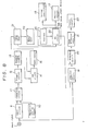
- the reference numeral 31 indicates a first delay line.
- the first delay line has provided therein, for example, plural delay terminals of stepwisely different inductances. These delay terminals are selectively used by a changeover switch provided outside the delay line. An output pulse supplied from the AND circuit 14 to an IN terminal thus selected is delivered as delayed a selected time.
- the delay time can be freely set as selected from a wide range from second x 10 12 ( P sec) to second x 10 3 (M sec) through selection of a delay line.
- a setting range is selected which is suitable for the kind of an object under flaw detection and it is divided to a plurality of steps, for example, about 10 steps, which are selectable by means of the above-mentioned external changeover switch.
- the reference numeral 32 indicates a second delay line which, similarly to the first delay line 31, has plural delay terminals of stepwisely different inductances. Any of these delay terminals is freely selected by means of the above-mentioned external changeover switch to delay a selected time an output pulse delivered from the Q terminal of the multivibrator 16a in the gate circuit 16.
- the first delay line 31 and second delay line 32 are a single line, respectively, for they provide each a delay time suitable for flaw detection.
- the reference numeral 23 indicates a NAND gate which are applied with both output pulses from the multivibrator 16a of the gate circuit 16 and the second delay line 32 to provide an inverted AND pulse, and 24 indicates an inverter which inverts the output pulse from the NAND circuit 23 to delivers it as gate pulse.
- the gate pulse is supplied to the monitor circuit 17, monitor sync circuit 18 and detection input circuit 19, respectively.
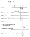
- (a) indicates an example echo pattern of the reflected wave from the object.
- a surface echo S and flaw echo F appear in the proximity of each other.
- the echoes correspond to surface flaws or flaws included in an extremely thin object.
- L indicates a line indicating a threshold for the levels of a transmitted pulse and various echoes. Assume now that the level of a transmitted pulse T exceeds the threshold L.
- the delayed trigger circuit 13 is tripped to set a delayed trigger pulse (b) and at the same time, an echo (a) from the object 3, which is receivered by the receiver circuit 6, is supplied to the input circuit 9.
- the output signal from the input circuit 9 is supplied to the trigger circuit 12 via the comparison circuit 11.
- a trigger signal is provided.
- the trigger signal is supplied to the AND circuit from which it is delivered as ANDed with the above-mentioned delayed trigger pulse also supplied to the AND circuit 14 and a pulse derived from the delayed trigger pulse having passed through a D type flip-flop.
- This output pulse is an AND circuit output pulse (c) which rises when the level of the surface echo S exceeds the threshold L.
- any 'one of the plural delay terminals can be freely selected by means of the external changeover switch, the above-mentioned input pulse is delivered as a first pulse (d) delayed a selected time t d1 at the selected delay terminal.
- the first output pulse thus delivered is supplied to the gate circuit 16 to apply the gate circuit reference output pulse (e) set to a predetermined width by the multivibrator 16a, resistor and capacitor in the gate circuit 16 to the NAND circuit 23 of the gate pulse output device 33.
- the Q terminal of the multivibrator 16a delivers an inverted gate circuit reference output pulse to the second delay line 32.
- any one of the delay terminals of the second delay line 32 is freely selected by means of the external changeover switch, thereby delivering the input pulse to the second delay line 32 as a second pulse (f) delayed a selected time t d2 and applying this output pulse to the NAND circuit 23.
- the NAND circuit 23 delivers a NAND circuit output pulse (g) of inverted AND.
- This output pulse is inverted by the inverter 24 to provide an inverter output pulse (h) having a pulse width P G , that is, gate pulse.
- the aforementioned delay time t dl and t d2 vary depending on the flaw detecting conditions and kind of the object under flaw detection as having previously been described. However, since a delay line and setting range of its delay time suitable for the flaw detecting conditions and kind of the object can be freely selected and the delay time can be freely changed from one to another, the delay time t d1 can be set freely and easily according to the relative time points where the surface echo S and flaw echo F appear, while the delay time t d2 can be set freely and easily according to a time during which the flaw echo F appears. In this case, the delay time t d1 is set to a time including the previously mentioned delay time t PLH for propagation in the multivibrators, etc.
- the gate pulse turns on at a point where the first pulse (d) is generated as delayed a time from when the level of the surface echo S has exceeded the threshold L until the gate circuit reference output pulse (e) rise, that is, a time t d1 due to the first delay line 31. Also, the gate pulse turns off at a position where the second pulse (f) is generated as delayed a time t d2 due to the second delay line 32 from when the gate circuit reference output pulse has fallen.
- the gate pulse will turn on when a delay time t dl passes after the level of the surface echo S has exceeded the threshold L, and it will turn off when a further delay time t d2 passes after that.
- the width P G of the gate pulse is equal to the delay time t d2 in view of the above relation and is increased or decreased proportionally to the delay time td2, it can be freely and easily set to a width corresponding to a time during which the flaw echo F appears before and after the peak of the flaw echo (the peak included) as shown in Fig. 5.
- the above-mentioned delay time t d1 and t d2 and gate pulse width P G will be affected by the accuracy of the delay time set by the delay lines, resulting a corresponding error, but this error of the delay time due to the delay lines is as small as about 5 ns though it-is slightly different from one length to another of the set delay time.
- the influence on the delay time t d1 and t d2 and gate pulse width P G is very small.
- the accuracy of the delay lines is such that even if the rise point of the gate circuit reference output pulse (e) is influenced by the delay time for internal propagation in the multivibrators of the gate circuit 16, output variation due to temperature change, etc.
- the delay time t d1 and t d2 are not influenced at all because the delay time error is small as mentioned above.
- the gate pulse it is possible to freely make the gate pulse appear at a selected point, that is, after a time of about 50 ns (a depth of about 150 ⁇ m from the surface of a steel object, for example) from a point where the level of the surface echo S has exceeded the threshold L, and also to shorten the gate pulse width P G from about 60 to 80 ns (which used to be the minimum limit) with the conventional techniques to, for example, about 30 ns.
- a gate pulse P G1 indicated with (b) in Fig. 7 is generated first for the flaw echo F 1 in a same processes as the processes (b) to (g) in Fig. 5.
- the circuit recovers the state before the trigger due to the flaw echo F 1 has been generated. So, a gate pulse P G2 indicated with (c) in Fig.
- a gate pulse P G3 can be generated for the further received flaw echo F 3 indicated with (d) in Fig. 7 in the same manner as for the flaw echoes F 1 and F 2 , thereby permitting to detect the flaws.
- the processes (b) to (g) shown in Fig. 5 are applied for the flaw echo F 2 .
- the gate pulse P G2 can be generated for the flaw echo F 2 independently of the flaw echoes F 1 and F 2 .
- FIG. 8 thru 10 the same elements as in Figs. 3 thru 5 are indicated with same reference numerals as in the latter Figures.
- FIGs. 8 and 9 the elements ranging from the input circuit 9 to the AND circuit 14 are the same as in Figs. 3 and 4 showing the first embodiment.
- the elements downstream of the AND circuit 14 are so arranged that the output from the AND circuit 14 is supplied to the first delay line 31 through the gate-circuit 16.
- the input pulse is delayed a selected time by the first delay line 32 and then delivered to the second delay line 32 and the AND circuit 26 forming a part of the gate pulse output device 33.
- the input pulse is delayed a selected time and delivered to the AND circuit through the inverter 25 forming together with the AND circuit 26 the gate pulse output device 33.
- the output pulse from the AND circuit 26, that is, a gate pulse, is delivered to the monitor circuit 17, monitor sync circuit 18 and detection input circuit 19.
- the elements ranging down to these circuits and the output circuit 22 are the same as in Fig. 3.
- the first pulse is supplied directly to the second delay line 32 in which it provides, as in the first delay line 31, a second pulse delayed a selected time t d2 from the point where the first pulse has been generated.
- the second pulse thus delivered is supplied to the inverter 25 to provide an inverter output pulse (g) which is supplied to the AND circuit 26.
- the inverter output pulse (g) is ANDED with the first pulse (e) to provide an AND circuit output pulse (h) having a width P G , that is, a gate pulse.
- the gate pulse indicated with (h) in Fig. 10 turns on at a point which is determined with the delay time due to the above-mentioned delay line which acts with a high accuracy (in this case, the first delay line 31). So the turn-on point of the gate pulse can be determined with a high accuracy and stability, which advantageously permits to detect the depth of a fine flaw accurately. Thus, the depth of the fine flaw can be effectively detected with a high accuracy.
- the delay time t dl and t d2 can be set freely and easily also in this embodiment as in the first embodiment.
- the relation between the delay time t dl and t d2 and the gate pulse is such that the gate pulse turns on when a delay time t d1 has passed after the level of the surface echo S has exceeded the threshold L and it turns off when a further delay time t d2 passes thereafter.
- the gate pulse width P G is equal to the delay time t d2 and increases/decrease proportionally to the delay time t d2 .
- the ultrasonic method and apparatus for flaw detection according to the present invention are not limited to the embodiments having been described in the foregoing, but they can be embodied in various forms without departing from the technical spirit of the present invention.
Landscapes
- Physics & Mathematics (AREA)
- Health & Medical Sciences (AREA)
- Life Sciences & Earth Sciences (AREA)
- Chemical & Material Sciences (AREA)
- Analytical Chemistry (AREA)
- Biochemistry (AREA)
- General Health & Medical Sciences (AREA)
- General Physics & Mathematics (AREA)
- Immunology (AREA)
- Pathology (AREA)
- Acoustics & Sound (AREA)
- Investigating Or Analyzing Materials By The Use Of Ultrasonic Waves (AREA)
Abstract
Dans ce dispositif, un signal de déclenchement est produit lorsque le niveau de l'écho de surface d'un échantillon à contrôler immergé dans un liquide dépasse une valeur de seuil prédéterminée, une première impulsion étant produite et retardée d'un laps de temps prédéterminé (td1) via une première ligne de retard (31) après la position où le signal de déclenchement est produit, une impulsion de porte est ouverte par la montée de la première impulsion, une deuxième impulsion étant produite et retardée d'un laps de temps prédéterminé (td2) via une deuxième ligne de retard (32) après la position où la première impulsion monte, ladite impulsion de porte étant fermée à l'instant où la deuxième impulsion est produite, la largeur (Pc) de l'impulsion de porte obtenue devenant ainsi égale au temps de retard (td2) obtenu grâce à la deuxième ligne de retard, cette même largeur d'impulsion étant ensuite mise en corrélation avec la largeur d'un écho produit par les défectuosités des échantillons à contrôler.
Applications Claiming Priority (4)
| Application Number | Priority Date | Filing Date | Title |
|---|---|---|---|
| JP20946786 | 1986-09-08 | ||
| JP20946486 | 1986-09-08 | ||
| JP209464/86 | 1986-09-08 | ||
| JP209467/86 | 1986-09-08 |
Publications (1)
| Publication Number | Publication Date |
|---|---|
| EP0324855A1 true EP0324855A1 (fr) | 1989-07-26 |
Family
ID=26517468
Family Applications (1)
| Application Number | Title | Priority Date | Filing Date |
|---|---|---|---|
| EP87905793A Withdrawn EP0324855A1 (fr) | 1986-09-08 | 1987-09-07 | Procede et dispositif de detection aux ultrasons de defectuosites |
Country Status (3)
| Country | Link |
|---|---|
| EP (1) | EP0324855A1 (fr) |
| KR (1) | KR880701883A (fr) |
| WO (1) | WO1988002112A1 (fr) |
Cited By (1)
| Publication number | Priority date | Publication date | Assignee | Title |
|---|---|---|---|---|
| FR2697638A1 (fr) * | 1992-11-02 | 1994-05-06 | Asulab Sa | Appareil de mesure par ultrasons minimisant le nombre de valeurs numériques traitées par les moyens de traitement. |
Families Citing this family (1)
| Publication number | Priority date | Publication date | Assignee | Title |
|---|---|---|---|---|
| KR100679082B1 (ko) * | 1999-09-08 | 2007-02-05 | 주식회사 포스코 | 레이저 초음파를 이용한 내부결함 검출 장치 |
Family Cites Families (1)
| Publication number | Priority date | Publication date | Assignee | Title |
|---|---|---|---|---|
| US3262306A (en) * | 1962-09-19 | 1966-07-26 | Branson Instr | Ultrasonic testing system |
-
1987
- 1987-09-07 EP EP87905793A patent/EP0324855A1/fr not_active Withdrawn
- 1987-09-07 WO PCT/JP1987/000664 patent/WO1988002112A1/fr not_active Ceased
-
1988
- 1988-05-07 KR KR1019880700509A patent/KR880701883A/ko not_active Abandoned
Non-Patent Citations (1)
| Title |
|---|
| See references of WO8802112A1 * |
Cited By (3)
| Publication number | Priority date | Publication date | Assignee | Title |
|---|---|---|---|---|
| FR2697638A1 (fr) * | 1992-11-02 | 1994-05-06 | Asulab Sa | Appareil de mesure par ultrasons minimisant le nombre de valeurs numériques traitées par les moyens de traitement. |
| EP0596342A1 (fr) * | 1992-11-02 | 1994-05-11 | Asulab S.A. | Appareil de mesure par ultrasons minimisant le nombre de valeurs numériques traitées par les moyens de traitement |
| US5569853A (en) * | 1992-11-02 | 1996-10-29 | Asulab S.A. | Ultrasonic measuring apparatus which minimizes the number of digital values treated by processing means |
Also Published As
| Publication number | Publication date |
|---|---|
| KR880701883A (ko) | 1988-11-05 |
| WO1988002112A1 (fr) | 1988-03-24 |
Similar Documents
| Publication | Publication Date | Title |
|---|---|---|
| US3995212A (en) | Apparatus and method for sensing a liquid with a single wire transmission line | |
| US3929006A (en) | Measuring article thickness ultrasonically | |
| US2280226A (en) | Flaw detecting device and measuring instrument | |
| US4307616A (en) | Signal processing technique for ultrasonic inspection | |
| US4070917A (en) | Ultrasonic pulse-echo thickness and velocity measuring method | |
| JPS57175952A (en) | Non-destructive test device of non-metallic object by impulsive elastic wave | |
| US3827287A (en) | Methods of and apparatus for measuring the thickness of successive sections of a cable jacket | |
| US4003244A (en) | Ultrasonic pulse-echo thickness measuring apparatus | |
| US3916676A (en) | Method of and apparatus for measuring automatically successive sections of an elongated material | |
| US5201225A (en) | Instrument for measuring thickness of coated plate and method thereof | |
| US4098131A (en) | Method and apparatus for increasing the speed of ultrasonic pulse-echo testing | |
| US4064742A (en) | Ultrasonic inspection device | |
| US3999422A (en) | Ultrasonic test method and apparatus for testing thick-walled workpieces | |
| US2949028A (en) | Apparatus for ultrasonic materials testing | |
| US4492118A (en) | Nondestructive testing of structural material by means of ultrasonics | |
| JPS5737257A (en) | Bonding inspection apparatus | |
| US3624712A (en) | Ultrasonic pulse echo thickness-measuring device | |
| US4056971A (en) | Distance amplitude compensation system | |
| US5046363A (en) | Apparatus for rapid non-destructive measurement of die attach quality in packaged integrated circuits | |
| EP0336025B1 (fr) | Procédé et appareil de mesure utilisant la réflectométrie | |
| GB1332898A (en) | Nondestructive examination of materials | |
| JPH0552461B2 (fr) | ||
| RU2034236C1 (ru) | Ультразвуковой эхо-импульсный толщиномер | |
| JP3089643B2 (ja) | 電気機器の部分放電検出装置 | |
| JP2840656B2 (ja) | ピーク検出形超音波厚さ計 |
Legal Events
| Date | Code | Title | Description |
|---|---|---|---|
| PUAI | Public reference made under article 153(3) epc to a published international application that has entered the european phase |
Free format text: ORIGINAL CODE: 0009012 |
|
| 17P | Request for examination filed |
Effective date: 19890306 |
|
| AK | Designated contracting states |
Kind code of ref document: A1 Designated state(s): DE GB IT NL |
|
| STAA | Information on the status of an ep patent application or granted ep patent |
Free format text: STATUS: THE APPLICATION HAS BEEN WITHDRAWN |
|
| 18W | Application withdrawn |
Withdrawal date: 19900817 |