EP0325480B1 - Méthode et appareil d'analyse d'un signal optique utilisant une source de modulation déclenchée et un circuit optique à retard pour réaliser un récepteur homodyne - Google Patents
Méthode et appareil d'analyse d'un signal optique utilisant une source de modulation déclenchée et un circuit optique à retard pour réaliser un récepteur homodyne Download PDFInfo
- Publication number
- EP0325480B1 EP0325480B1 EP89300554A EP89300554A EP0325480B1 EP 0325480 B1 EP0325480 B1 EP 0325480B1 EP 89300554 A EP89300554 A EP 89300554A EP 89300554 A EP89300554 A EP 89300554A EP 0325480 B1 EP0325480 B1 EP 0325480B1
- Authority
- EP
- European Patent Office
- Prior art keywords
- optical
- source
- modulation
- optical signal
- signal produced
- Prior art date
- Legal status (The legal status is an assumption and is not a legal conclusion. Google has not performed a legal analysis and makes no representation as to the accuracy of the status listed.)
- Expired - Lifetime
Links
- 230000003287 optical effect Effects 0.000 title claims description 272
- 238000000034 method Methods 0.000 title claims description 21
- 238000004458 analytical method Methods 0.000 title description 3
- 238000001228 spectrum Methods 0.000 claims description 32
- 238000010183 spectrum analysis Methods 0.000 claims description 18
- 230000003111 delayed effect Effects 0.000 claims description 6
- 239000013307 optical fiber Substances 0.000 claims description 6
- 238000001514 detection method Methods 0.000 claims description 4
- 230000003595 spectral effect Effects 0.000 claims description 4
- 238000013459 approach Methods 0.000 claims description 2
- 238000005259 measurement Methods 0.000 description 12
- 239000000835 fiber Substances 0.000 description 6
- 238000002044 microwave spectrum Methods 0.000 description 6
- 238000004891 communication Methods 0.000 description 2
- 238000010586 diagram Methods 0.000 description 2
- 239000006185 dispersion Substances 0.000 description 2
- 239000004065 semiconductor Substances 0.000 description 2
- 238000012360 testing method Methods 0.000 description 2
- 229910000530 Gallium indium arsenide Inorganic materials 0.000 description 1
- 238000012512 characterization method Methods 0.000 description 1
- 230000001934 delay Effects 0.000 description 1
- 238000002347 injection Methods 0.000 description 1
- 239000007924 injection Substances 0.000 description 1
- 238000005305 interferometry Methods 0.000 description 1
- 230000002045 lasting effect Effects 0.000 description 1
- 238000012546 transfer Methods 0.000 description 1
Images


Classifications
-
- G—PHYSICS
- G01—MEASURING; TESTING
- G01J—MEASUREMENT OF INTENSITY, VELOCITY, SPECTRAL CONTENT, POLARISATION, PHASE OR PULSE CHARACTERISTICS OF INFRARED, VISIBLE OR ULTRAVIOLET LIGHT; COLORIMETRY; RADIATION PYROMETRY
- G01J9/00—Measuring optical phase difference; Determining degree of coherence; Measuring optical wavelength
- G01J9/04—Measuring optical phase difference; Determining degree of coherence; Measuring optical wavelength by beating two waves of a same source but of different frequency and measuring the phase shift of the lower frequency obtained
Definitions
- This invention relates to optical spectrum analysis and, more particularly, to measurement of the spectrum of a modulated optical signal.
- the invention is directed to a method and apparatus for measurement of the spectrum of a modulated optical signal using a gated modulation source and a self-homodyne detection method based on the use of an optical delay circuit for recovering the optical field spectrum on a modulated optical signal.
- the power spectrum of an optical source determines the performance of any optical device, such as a fiber optic system or associated component, that operates on that source. For example, if a laser transmitter feeds into an optical fiber cable for a link to an optical receiver elsewhere in a fiber optic system, the power spectrum of the laser determines the amount of pulse distortion due to dispersion in the optical fiber and thus the effectiveness of the communication link.
- Another known technique utilizes a scanning Fabry Perot spectrometer.
- this spectrometer has limited dynamic frequency range if operated over a wide spectral band.
- a detector at the output of the interferometer acts as an optical product detector.
- the modulation is constrained to be a square wave, and the modulation rate is tied to the delay in the optical circuit, so that the square wave has a period of twice the delay.
- a method for directly analysing the optical field spectrum of an optical signal based on a local oscillator approach for mixing down the actual optical field spectrum to baseband including the steps of providing an optical source, providing a modulation source for modulating the optical signal produced by the optical source, routing the optical signal produced by the optical source to an optical circuit for providing delayed and undelayed states of the optical signal, recombining the states of the optical signal produced by the optical source together concurrently after being channelled through the optical circuit, and mixing the recombined states of the optical signal produced by the optical source, characterised in that the step of providing a modulation source for modulating the optical signal produced by the optical source comprises: providing a modulation source for modulating the optical signal produced by the optical source so that the
- an optical spectrum analysis system comprising an optical source for producing an optical signal, a modulation source connected to the optical source for modulating the optical signal produced by the optical source, a first optical power splitter connected to the optical source for splitting the optical signal produced by the optical source, an optical conduit having an input and an output, the input of the optical conduit being connected to the first optical power splitter, an optical delay line having an input and an output and a predetermined time delay, the input of the optical delay line also being connected to the first optical power splitter, a second optical power splitter for recombining the optical signal produced by the optical source, the output of the optical conduit and the output of the optical delay line being connected to the second optical power splitter, characterised in that: the modulation source generates a gate function employed as a trigger signal to gate a modulation signal applied to the optical signal produced by the optical source, thereby producing a gated modulation signal for modulating the optical signal produced by the optical source so that the optical signal produced by the optical source alternates between
- the method and apparatus of the invention are essentially wavelength independent (limited only by detectors and fiber components >300 nm). Additionally, no tracking of an additional local oscillator is required. Furthermore, unlike known optical spectrum analysis systems, including the one disclosed in the aforementioned Abitbol et al. , article, high frequency modulation is applied when the modulation source is gated on by a gate function to provide gated modulation of the optical signal produced by the optical source, i.e., there is modulation under the gate function. This modulation can be at any frequency greater than the gate frequency, rather than the modulation rate being tied to the delay of the optical delay line.
- the invention allows direct measurement of the optical field spectrum on an optical signal.
- a single optical source such as a laser, is used to frequency-translate the optical power spectrum to within the bandwidth of an analyzer, such as a microwave spectrum analyzer. This is achieved by alternating, or switching, the optical signal produced by the optical source between two states, namely, an unmodulated state, which is used in lieu of a local oscillator signal, and a modulated state, which carries the optical field spectrum of interest, and by mixing these states in a self-homodyne receiver which includes an optical delay circuit.
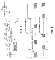
- Fig. 1 is a schematic diagram of an optical spectrum analysis system in accordance with one embodiment of the invention, generally indicated by the numeral 10.
- the optical spectrum analysis system 10 comprises an optical source 12 for producing an optical signal.
- the optical source 12 can be, for example, a laser, such as a DFB laser.
- the optical spectrum analysis system 10 further comprises a modulation source 14 connected to the optical source 12.
- the modulation source 14 is preferably a gated modulator which produces bursts of modulation. Accordingly, as shown in Fig. 2, the modulation source 14 generates a gate function 16 which is employed as a trigger signal to gate a modulation signal 18, thereby producing a gated modulation signal 20.
- the modulation signal 18 on which the gate function 16 is superimposed can be continuous wave, pulse, pseudorandom bit sequence (PRBS), or other type of modulation.
- PRBS pseudorandom bit sequence
- the gated modulation signal 20 preferably has a 50% duty cycle and a period 2T, as shown in Fig. 2.
- the relationship between the frequency of modulation and gate frequency is: f m > f GATE
- the gated modulation signal 20 produced by the modulation source 14 modulates the optical signal produced by the optical source 12.
- the optical signal produced by the optical source 12 alternates between two states, namely, an unmodulated state, as shown in Fig. 3A, and a modulated state which carries the optical field spectrum of interest, as shown in Fig. 3B.
- the optical spectrum analysis system 10 further comprises a first optical power splitter 22 connected to the optical source 12.
- the optical spectrum analysis system 10 also comprises an optical conduit 24, whose input is connected to the first optical power splitter 22, and an optical delay line 26, whose input is also connected to the first optical power splitter.
- the optical conduit 24 can be optical fiber cable or, alternatively, the atmosphere, i.e., free space.
- the optical delay line 26 comprises a predetermined length of optical fiber cable.
- the output of the optical conduit 24 and the output of the optical delay line 26 are connected to a second optical power splitter 28 also included in the optical spectrum analysis system 10. Therefore, the optical conduit 24 and the optical delay line 26 are connected in a parallel optical circuit.
- the optical spectrum analysis system 10 further comprises a photodetector 30.
- the photodetector 30 can be a photodiode.
- the detection bandwidth of the photodetector 30 is wider than the AM and FM bandwidths.
- the optical spectrum analysis system 10 preferably comprises an analyzer 32, such as a microwave spectrum analyzer or RF spectrum analyzer.
- the combination of the first optical power splitter 22, optical conduit 24, optical delay line 26, second optical power splitter 28, and photodetector 30 forms a self-homodyne receiver in response to the alternately unmodulated and modulated optical signal produced by the optical source 12 shown in Fig. 3, as will now be described.
- the unmodulated optical signal produced by the optical source 12 is used in lieu of a local oscillator signal.
- E A (t) be the optical signal which passes through the optical conduit 24 and E B (t) be the optical signal which passes through the optical delay line 26.
- An illustration of E A (t) appears in Fig. 4A and of E B (t) appears in Fig. 4B.
- E A (t) and E B (t) alternately serve as the local oscillator signal and the modulated optical signal.
- the field E O is composed of two parts, one due to the modulated optical signal produced by the optical source and another due to the unmodulated optical signal. Therefore, the signal current I D in the photodetector 30 is proportional to: E A (t)2 + E B (t)2 + 2[E A (t) ⁇ E B (t)]
- the first two terms represent optical intensity modulation.
- the last term gives the spectral information of interest.
- E A (t) is the unmodulated optical signal produced by the optical source 12 currently serving as the local oscillator signal
- E B (t) is the modulated optical signal with both AM and FM imparted on it
- the third term (which is proportional to E A (t) ⁇ E B (t)) in the above expression effectively represents the mixing between the equivalent of a local oscillator signal and the unknown signal. This results in a measurement whose resolution is a function of the unmodulated linewidth of the optical source 12, such as a laser, and the interferometer transfer function of the optical conduit 24 and the optical delay line 26.
- the optical spectrum analysis system 10 can directly measure the chirp a laser undergoes during IM modulation.
- the laser modulation is preferably gated by a square wave of period twice the differential delay of the optical circuit.
- the gate function 16 When the gate function 16 is on, modulated signal is allowed to pass to the laser.
- the result is that two optical beams, one unmodulated and the other modulated, are mixed, thereby yielding a term associated with laser chirp directly.
- Another important measurement, useful in determining the dispersion over a fiber link, is that of the spectrum of the optical field of a current modulated DFB laser.
- the method and apparatus in accordance with the invention use the optical delay line 26 combined with gated modulation to measure the homodyne power spectrums of both the optical field and intensity of a DFB laser under normal operating conditions.
- the mixing of a modulated DFB laser with a CW local oscillator is achieved with a single laser by using gated modulation combined with an appropriate optical delay to perform frequency chirp measurements up to +/- 22 GHz.
- Detecting the mixed optical signal with a wide bandwidth analyzer 32 i.e., optical detector, preamplifier, and microwave spectrum analyzer allows direct observation of frequency chirps.
- a DFB laser provides the optical source 12 and is switched between two states of operation, each state lasting a time T.
- the laser operates as a CW local oscillator.
- any desired AC-coupled modulation can be applied to the laser.
- the time T is assumed to be much longer than the period of the modulation.
- the laser signal is then fed to the first optical power splitter 22 and, hence, to the parallel optical circuit comprising the optical conduit 24 and the optical delay line 26, whose differential time delay T results in the continuous addition of the modulated and unmodulated laser states in the second power splitter 28.
- This circuit together with the photodetector 30 effectively acts as an optical homodyne receiver where a modulated laser signal is mixed with a CW local oscillator signal, but without the constraint of requiring two separate lasers.
- the resulting power spectrum of the output photocurrent is composed of two components.
- the first is a direct feedthrough term associated with the gated intensity modulation of the laser.
- the second term is the result of optical mixing between the unmodulated and modulated laser states. This second term provides for the direct observation of the frequency excursions on the optical signal produced by the laser. In practice, these two terms are easily distinguished, since the intensity modulation terms are spectrally narrow, while the terms associated with the optical FM spectrum are broadened due to the laser linewidth.
- the signal produced by the photodetector 30 was fed to the analyzer 32, for example, a calibrated 100 kHz to 22 GHz microwave spectrum analyzer, such as a Model HP 71400A Lightwave Signal Analyzer available from Hewlett-Packard Company, Signal Analysis Division, Rohnert Park, California, comprising a high-speed InGaAs detector, microwave preamplifier, and microwave spectrum analyzer.
- the bandwidth of the electrical detection system was 22 GHz (+/- 0.12 nm at 1.3 um), which is well matched to typical frequency excursions attainable with DFB lasers.
- the DFB laser was measured under both sinusoidal and PRBS modulation. To help prevent thermally induced frequency chirps, the modulation source 14 was AC-coupled so that the average current to the laser remained constant during both halves of the gate period.
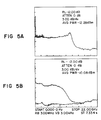
- Fig. 5 shows the power spectrum of the photocurrent in the photodetector 30 for the cases of sinusoidal and PRBS modulation.
- the modulation frequency was 100 MHz
- the DC bias current was 36 mA
- the modulation index was approximately 83%.
- the resulting frequency chirp of the laser was approximately +/-13 GHz, which corresponds to an FM modulation index of approximately 130.
- the discrete spectral components below 3 GHz are due to the direct feedthrough of the intensity modulation at the fundamental (100 MHz) and ItS various harmonics generated by non-linearities of the laser.
- the PRBS case Fig.
- the clock frequency was 350 MHz
- the bias current was 50 mA
- the modulation depth was about 20%
- the more gradual roll-off of the FM frequency chirp, compared to sinusoidal modulation, is believed to be due to the wider frequency spectrum of the PRBS modulation.
- the bottom trace in Fig. 5B is the noise floor of the analyzer 32 with the optical signal blocked.
- Fig. 6 shows plots of maximum frequency chirp versus modulation index of the DFB laser.
- the method and apparatus in accordance with the invention can directly measure the homodyne power spectrum of the optical field for a modulated DFB laser.
- Various other uses will also appear to persons skilled in the art.
Landscapes
- Physics & Mathematics (AREA)
- Spectroscopy & Molecular Physics (AREA)
- General Physics & Mathematics (AREA)
- Optical Communication System (AREA)
- Spectrometry And Color Measurement (AREA)
Claims (19)
- Procédé d'analyse directe du spectre de champ optique d'un signal optique basé sur une approche d'oscillateur local pour mélanger le spectre de champ optique réel à la bande de base, comprenant les étapes de fournir une source optique (12), de fournir une source de modulation (14) pour moduler le signal optique fourni par la source optique (12), diriger le signal optique produit par la source optique (12) vers un circuit optique (24, 26) pour fournir des états retardés et non retardés du signal optique, recombiner les états du signal optique produit par la source optique (12) concuremment après les avoir fait passer dans un circuit optique (24, 26) et mélanger les états recombinés du signal optique produit par la source optique (12), caractérisé en ce que l'étape de fournir une source de modulation (14) pour moduler le signal optique produit par la source optique (12) comprend :- de fournir une source de modulation (14) pour moduler le signal optique produit par la source optique (12) de sorte que le signal optique produit par la source optique (12) alterne entre a) un état non modulé et b) un état modulé qui porte le spectre de champ optique intéressant ;- l'état non modulé du signal optique produit par la source optique (12) servant de signal oscillateur local ;- fournir ainsi le mélange homodyne des états non modulé et modulé du signal optique produit par la source optique (12).
- Procédé de la revendication 1 dans lequel le circuit optique (24, 26) a un retard différentiel entre l'état retardé et l'état non retardé du signal optique et la durée de chaque état non modulé et modulé est égale au retard différentiel du circuit optique (24, 26).
- Procédé de la revendication 1 dans lequel le circuit optique (24, 26) a un retard différentiel entre les états retardés et non retardés du signal optique et la durée de chacun des états non modulé et modulé est une fraction entière du retard différentiel du circuit optique (24, 26).
- Procédé selon l'une quelconque des revendications précédentes dans lequel on applique une modulation de fréquence élevée à l'aide de la source de modulation (14) au signal optique produit par la source optique (12) quand la source de modulation (14) est déclenchée par une fonction de déclenchement pour fournir une modulation déclenchée du signal optique produit par la source optique (12).
- Procédé de la revendication 4 dans lequel le circuit optique (24, 26) a un retard différentiel entre les états retardé et non retardé du signal optique et la modulation à toute fréquence est supérieure à la fréquence de déclenchement.
- Procédé selon l'une quelconque des revendications précédentes dans lequel l'étape de mélange des états recombinés du signal optique produit par la source optique (12) comprend le mélange des états recombinés du signal optique produit par la source optique (12) dans un photodétecteur (30), ce qui réalise le mélange en réponse aux états non modulé et modulé du signal optique produit par la source optique (12).
- Procédé de la revendication 6 dans lequel le mélange des états non modulé et modulé du signal optique produit par la source optique (12) transfère en fréquence le spectre de puissance optique dans la largeur de bande d'un analyseur (32).
- Système d'analyse de spectre optique comprenant une source optique (12) pour produire un signal optique, une source de modulation (14) connectée à la source optique (12) pour moduler le signal optique produit par la source optique (12), un premier séparateur de puissance optique (22) connecté à la source optique (12) pour partager le signal optique produit par la source optique (12), un conducteur optique (24) ayant une entrée et une sortie, l'entrée du conducteur optique (24) étant connectée au premier séparateur de puissance optique (22), une ligne de retard optique (26) ayant une entrée et une sortie et un retard de temps fixé, l'entrée de la ligne de la ligne de retard optique (26) étant aussi branchée au premier séparateur (22) de puissance optique, un deuxième séparateur de puissance optique (28) est prévu pour recombiner le signal produit par la source optique (12), la sortie du conducteur optique (24) et la sortie de la ligne de retard optique (26) étant branchées au second séparateur de puissance optique (28), caractérisé en ce que :- la source de modulation (14) génère une fonction de déclenchement utilisée comme signal gâchette pour déclencher un signal de modulation appliqué au signal optique produit par la source optique (12), produisant ainsi un signal de modulation déclenchée pour moduler le signal optique produit par la source optique (12) de sorte que le signal optique produit par la source optique (12) alterne entre a) un état non modulé et b) un état modulé qui porte un spectre de champ optique intéressant ;- le premier séparateur de puissance optique (22) fractionne le signal optique alternativement non modulé et modulé produit par la source optique (12) ; et- le second séparateur de puissance optique (28) recombine le signal optique alternativement non modulé et modulé produit par la source optique (12) ;- le signal optique non modulé produit par la source optique (12) est utilisé à la place d'un signal oscillateur local.
- Système de la revendication 8 dans lequel la source de modulation est un modulateur déclenché qui produit des bouffées de modulation.
- Système de la revendication 8 ou 9 dans lequel le signal de modulation sur lequel la fonction de déclenchement est superposée est sélectionné parmi une modulation par onde continue, impulsion et séquence pseudoaléatoire de bits.
- Système selon l'une quelconque des revendications 8 à 10 dans lequel le circuit optique (24, 26) a un retard différentiel entre la sortie du circuit optique provenant du circuit optique (24) et la sortie du signal optique provenant de la ligne de retard optique (26) et la source de modulation (14) génère un signal de modulation déclenché ayant un cycle de service de 50% et une période double du retard différentiel du circuit optique (24, 26).
- Système selon l'une quelconque des revendications 8 à 11, dans lequel la relation entre la fréquence de modulation appliquée à la source de modulation (14) et la fréquence de déclenchement est fm > fGATE.
- Système selon l'une quelconque des revendications 8 à 12 dans lequel le conducteur optique est choisi parmi un câble à fibre optique et l'atmosphère.
- Système selon l'une quelconque des revendications 8 à 13 dans lequel la ligne de retard optique comprend une longueur prédéterminée de câble de fibre optique.
- Système selon l'une quelconque des revendications 8 à 14, dans lequel la relation entre la fréquence de déclenchement et le retard à durée prédéterminée de la ligne à retard optique est

- Système selon l'une quelconque des revendications 8 à 15, qui comprend en outre un photodétecteur (30), la combinaison du premier séparateur de puissance optique (22), du conducteur optique (24), de la ligne de retard optique (26), du second séparateur de puissance optique (28), et du photodétecteur (30) formant un récepteur en réponse au signal alternativement non modulé et modulé produit par la source optique (12).
- Système selon la revendication 16, dans lequel
- Système selon la revendication 16 ou 17, dans lequel, pendant un temps T, EA(t) est le signal optique non modulé produit par la source optique (12) servant habituellement de signal oscillant local et EB(t) est le signal optique modulé avec à la fois des AM et FM, le photodétecteur (30) produit un courant de signal ID proportionnel à

- Système selon l'une quelconque des revendications 16 à 18, comprenant en plus un analyseur (32) pour afficher le spectre de puissance du signal optique.
Applications Claiming Priority (2)
| Application Number | Priority Date | Filing Date | Title |
|---|---|---|---|
| US146915 | 1988-01-22 | ||
| US07/146,915 US4859843A (en) | 1988-01-22 | 1988-01-22 | Method and apparatus for optical signal analysis using a gated modulation source and an optical delay circuit to achieve a self-homodyne receiver |
Publications (3)
| Publication Number | Publication Date |
|---|---|
| EP0325480A2 EP0325480A2 (fr) | 1989-07-26 |
| EP0325480A3 EP0325480A3 (fr) | 1991-04-24 |
| EP0325480B1 true EP0325480B1 (fr) | 1994-06-01 |
Family
ID=22519552
Family Applications (1)
| Application Number | Title | Priority Date | Filing Date |
|---|---|---|---|
| EP89300554A Expired - Lifetime EP0325480B1 (fr) | 1988-01-22 | 1989-01-20 | Méthode et appareil d'analyse d'un signal optique utilisant une source de modulation déclenchée et un circuit optique à retard pour réaliser un récepteur homodyne |
Country Status (4)
| Country | Link |
|---|---|
| US (1) | US4859843A (fr) |
| EP (1) | EP0325480B1 (fr) |
| JP (1) | JP2842882B2 (fr) |
| DE (1) | DE68915553T2 (fr) |
Families Citing this family (5)
| Publication number | Priority date | Publication date | Assignee | Title |
|---|---|---|---|---|
| US5319438A (en) * | 1992-01-24 | 1994-06-07 | Board Of Regents, The University Of Texas System | Interferometric, self-homodyne optical receiver and method and optical transmission system incorporating same |
| FR2689632B1 (fr) * | 1992-04-02 | 1997-09-19 | Thomson Csf | Detecteur a fibre optique de contraintes. |
| US7283572B2 (en) * | 2004-01-15 | 2007-10-16 | Ben Gurion University Of The Negey | Measurement of wavelength transients in tunable lasers |
| US10050713B2 (en) * | 2015-03-02 | 2018-08-14 | Futurewei Technologies, Inc. | Optical transceiver using duplex media, self-homodyne detection (SHD), coherent detection, and uncooled laser |
| CN112505408B (zh) * | 2020-11-19 | 2022-02-08 | 中国电子科技集团公司第三十研究所 | 一种微波光子测频装置与方法 |
Family Cites Families (3)
| Publication number | Priority date | Publication date | Assignee | Title |
|---|---|---|---|---|
| US4725774A (en) * | 1986-06-20 | 1988-02-16 | Northrop Corporation | Integrated interferometric acousto-optic spectrum analyzer |
| US4768880A (en) * | 1986-06-23 | 1988-09-06 | The Board Of Trustees Of The Leland Stanford Junior University | System and method for accurate loop length determination in fiber-optic sensors and signal processors |
| GB2192272B (en) * | 1986-07-02 | 1990-06-06 | Cossor Electronics Ltd | Spectrum analyser |
-
1988
- 1988-01-22 US US07/146,915 patent/US4859843A/en not_active Expired - Lifetime
-
1989
- 1989-01-20 EP EP89300554A patent/EP0325480B1/fr not_active Expired - Lifetime
- 1989-01-20 DE DE68915553T patent/DE68915553T2/de not_active Expired - Fee Related
- 1989-01-20 JP JP1011789A patent/JP2842882B2/ja not_active Expired - Fee Related
Also Published As
| Publication number | Publication date |
|---|---|
| EP0325480A3 (fr) | 1991-04-24 |
| JPH01308971A (ja) | 1989-12-13 |
| JP2842882B2 (ja) | 1999-01-06 |
| DE68915553D1 (de) | 1994-07-07 |
| EP0325480A2 (fr) | 1989-07-26 |
| DE68915553T2 (de) | 1994-09-15 |
| US4859843A (en) | 1989-08-22 |
Similar Documents
| Publication | Publication Date | Title |
|---|---|---|
| Domingo et al. | Very high resolution optical spectrometry by stimulated Brillouin scattering | |
| Baney et al. | Coherent optical spectrum analyzer | |
| US4594511A (en) | Method and apparatus for double modulation spectroscopy | |
| JP3498141B2 (ja) | 光パルス評価方法、光パルス評価装置、及び光通信システム | |
| US6057919A (en) | Apparatus and method for measuring characteristics of optical pulses | |
| Szafraniec et al. | Swept coherent optical spectrum analysis | |
| US12392810B2 (en) | Device for wide-band spectral analysis of a signal of interest | |
| US7405820B2 (en) | Optical spectrum analyzing device by means of Brillouin scattering and associated measurement process | |
| Tsuji et al. | Spatial-resolution improvement in long-range coherent optical frequency domain reflectometry by frequency-sweep linearisation | |
| EP4460679B1 (fr) | Système de mesure optique | |
| US5256968A (en) | Measurement of high-frequency electrical signals by electro-optical effect | |
| Tsuji et al. | Coherent optical frequency domain reflectometry using phase-decorrelated reflected and reference lightwaves | |
| Reisinger et al. | Coherence of a room-temperature cw GaAs/GaAlAs injection laser | |
| JP3805555B2 (ja) | レーザ周波数測定方法、レーザ周波数制御方法、レーザ周波数測定装置及びレーザ光発生装置 | |
| US4859843A (en) | Method and apparatus for optical signal analysis using a gated modulation source and an optical delay circuit to achieve a self-homodyne receiver | |
| US7023556B2 (en) | Method and apparatus for measurement of group delay | |
| JPH05322695A (ja) | 光パルス試験器 | |
| JP3223439B2 (ja) | ファイバ検査装置 | |
| Campbell et al. | Measurement of the modulation efficiency of an optical phase modulator using a self-homodyne receiver | |
| Preussler et al. | Optical spectrum analysis with kHz resolution based on polarization pulling and local oscillator assisted Brillouin scattering | |
| JPH0540075A (ja) | 光パルス試験器 | |
| Andersson et al. | A Fourier transform spectrometer for high resolution measurements of static and dynamic spectra of semiconductor lasers | |
| Wong et al. | Digitally Enhanced Homodyne Dispersion Spectrometer | |
| Brunner et al. | Tunable diode laser line width and tuning measurements for gas analysis monitoring | |
| Tsuji et al. | Spatial-resolution improvement in coherent optical frequency domain reflectometry for long optical fibers by reducing frequency-sweep nonlinearity |
Legal Events
| Date | Code | Title | Description |
|---|---|---|---|
| PUAI | Public reference made under article 153(3) epc to a published international application that has entered the european phase |
Free format text: ORIGINAL CODE: 0009012 |
|
| AK | Designated contracting states |
Kind code of ref document: A2 Designated state(s): DE FR GB |
|
| PUAL | Search report despatched |
Free format text: ORIGINAL CODE: 0009013 |
|
| AK | Designated contracting states |
Kind code of ref document: A3 Designated state(s): DE FR GB |
|
| 17P | Request for examination filed |
Effective date: 19911017 |
|
| 17Q | First examination report despatched |
Effective date: 19930205 |
|
| GRAA | (expected) grant |
Free format text: ORIGINAL CODE: 0009210 |
|
| AK | Designated contracting states |
Kind code of ref document: B1 Designated state(s): DE FR GB |
|
| REF | Corresponds to: |
Ref document number: 68915553 Country of ref document: DE Date of ref document: 19940707 |
|
| ET | Fr: translation filed | ||
| PLBE | No opposition filed within time limit |
Free format text: ORIGINAL CODE: 0009261 |
|
| STAA | Information on the status of an ep patent application or granted ep patent |
Free format text: STATUS: NO OPPOSITION FILED WITHIN TIME LIMIT |
|
| 26N | No opposition filed | ||
| REG | Reference to a national code |
Ref country code: GB Ref legal event code: 732E |
|
| REG | Reference to a national code |
Ref country code: GB Ref legal event code: 732E |
|
| REG | Reference to a national code |
Ref country code: FR Ref legal event code: TP |
|
| REG | Reference to a national code |
Ref country code: FR Ref legal event code: TP |
|
| REG | Reference to a national code |
Ref country code: GB Ref legal event code: IF02 |
|
| PGFP | Annual fee paid to national office [announced via postgrant information from national office to epo] |
Ref country code: GB Payment date: 20060113 Year of fee payment: 18 |
|
| PGFP | Annual fee paid to national office [announced via postgrant information from national office to epo] |
Ref country code: FR Payment date: 20060117 Year of fee payment: 18 |
|
| PGFP | Annual fee paid to national office [announced via postgrant information from national office to epo] |
Ref country code: DE Payment date: 20060228 Year of fee payment: 18 |
|
| PG25 | Lapsed in a contracting state [announced via postgrant information from national office to epo] |
Ref country code: DE Free format text: LAPSE BECAUSE OF NON-PAYMENT OF DUE FEES Effective date: 20070801 |
|
| GBPC | Gb: european patent ceased through non-payment of renewal fee |
Effective date: 20070120 |
|
| REG | Reference to a national code |
Ref country code: FR Ref legal event code: ST Effective date: 20070930 |
|
| PG25 | Lapsed in a contracting state [announced via postgrant information from national office to epo] |
Ref country code: GB Free format text: LAPSE BECAUSE OF NON-PAYMENT OF DUE FEES Effective date: 20070120 |
|
| PG25 | Lapsed in a contracting state [announced via postgrant information from national office to epo] |
Ref country code: FR Free format text: LAPSE BECAUSE OF NON-PAYMENT OF DUE FEES Effective date: 20070131 |