EP0326187A2 - Structure MOSFET à puissance - Google Patents
Structure MOSFET à puissance Download PDFInfo
- Publication number
- EP0326187A2 EP0326187A2 EP89104187A EP89104187A EP0326187A2 EP 0326187 A2 EP0326187 A2 EP 0326187A2 EP 89104187 A EP89104187 A EP 89104187A EP 89104187 A EP89104187 A EP 89104187A EP 0326187 A2 EP0326187 A2 EP 0326187A2
- Authority
- EP
- European Patent Office
- Prior art keywords
- epitaxial layer
- conductivity type
- region
- opening
- type
- Prior art date
- Legal status (The legal status is an assumption and is not a legal conclusion. Google has not performed a legal analysis and makes no representation as to the accuracy of the status listed.)
- Withdrawn
Links
Images

Classifications
-
- H—ELECTRICITY
- H10—SEMICONDUCTOR DEVICES; ELECTRIC SOLID-STATE DEVICES NOT OTHERWISE PROVIDED FOR
- H10W—GENERIC PACKAGES, INTERCONNECTIONS, CONNECTORS OR OTHER CONSTRUCTIONAL DETAILS OF DEVICES COVERED BY CLASS H10
- H10W20/00—Interconnections in chips, wafers or substrates
- H10W20/40—Interconnections external to wafers or substrates, e.g. back-end-of-line [BEOL] metallisations or vias connecting to gate electrodes
-
- H—ELECTRICITY
- H10—SEMICONDUCTOR DEVICES; ELECTRIC SOLID-STATE DEVICES NOT OTHERWISE PROVIDED FOR
- H10D—INORGANIC ELECTRIC SEMICONDUCTOR DEVICES
- H10D62/00—Semiconductor bodies, or regions thereof, of devices having potential barriers
- H10D62/10—Shapes, relative sizes or dispositions of the regions of the semiconductor bodies; Shapes of the semiconductor bodies
- H10D62/17—Semiconductor regions connected to electrodes not carrying current to be rectified, amplified or switched, e.g. channel regions
- H10D62/393—Body regions of DMOS transistors or IGBTs
-
- H—ELECTRICITY
- H10—SEMICONDUCTOR DEVICES; ELECTRIC SOLID-STATE DEVICES NOT OTHERWISE PROVIDED FOR
- H10D—INORGANIC ELECTRIC SEMICONDUCTOR DEVICES
- H10D64/00—Electrodes of devices having potential barriers
- H10D64/20—Electrodes characterised by their shapes, relative sizes or dispositions
- H10D64/23—Electrodes carrying the current to be rectified, amplified, oscillated or switched, e.g. sources, drains, anodes or cathodes
- H10D64/251—Source or drain electrodes for field-effect devices
- H10D64/252—Source or drain electrodes for field-effect devices for vertical or pseudo-vertical devices
- H10D64/2527—Source or drain electrodes for field-effect devices for vertical or pseudo-vertical devices for vertical devices wherein the source or drain electrodes are recessed in semiconductor bodies
-
- H—ELECTRICITY
- H10—SEMICONDUCTOR DEVICES; ELECTRIC SOLID-STATE DEVICES NOT OTHERWISE PROVIDED FOR
- H10D—INORGANIC ELECTRIC SEMICONDUCTOR DEVICES
- H10D30/00—Field-effect transistors [FET]
- H10D30/60—Insulated-gate field-effect transistors [IGFET]
- H10D30/64—Double-diffused metal-oxide semiconductor [DMOS] FETs
- H10D30/66—Vertical DMOS [VDMOS] FETs
Definitions
- This invention relates to integrated circuit structures and in particular to an improved power metal oxide semiconductor field effect transistor (MOSFET) structure having higher switching speeds and improved breakdown characteristics.
- MOSFET metal oxide semiconductor field effect transistor
- MOSFET represents one of the first power semiconductor devices manufacturable using integrated circuit processing technology.
- a survey article discussing power MOSFET's is entitled "Switching Lots of Watts at High Speed" by B. Baliga, IEEE Spectrum , December 1981, pages 42-48.
- VDMOS complementary metal-oxide-semiconductor
- MOS devices fabricated using double diffusions in V-shaped grooves.
- conventionally fabricated VDMOS structures suffer from several disadvantages.
- Such devices are generally overly susceptible to secondary breakdown of parasitic bipolar transistors inherent in the structure.
- Such structures typically have undesirably large drain to source resistance when on.
- the devices switch at undesirably low speeds in view of their relatively large size and therefore high gate capacitances.
- This invention provides a power MOSFET having improved performance characteristics over those of the prior art.
- this invention provides a power MOSFET structure which is less susceptible to secondary breakdown of parasitic transistors inherent in the integrated circuit structure, which has a lower drain to source resistance, which is capable of switching at higher speeds with lower gate capacitance than prior art devices.
- a semiconductor structure fabricated according to this invention includes a semiconductor drain region of first conductivity type having an upper surface; an opening in the drain region extending downward from the upper surface a selected distance; a source region of first conductivity type continguous to the opening and to the upper surface; a gate region of opposite conductivity type everywhere disposed between the source region and the drain region and extending to the surface of the drain region; a gate electrode disposed above all of the gate region and separated therefrom by insulating material, and means for providing electrical connections to the source region, the drain region, and the gate electrode.
- a method for fabricating the power MOSFET structure comprises the steps of forming an electrically conductive gate electrode on a semiconductor drain region of first conductivity type, the electrode being separated from the drain region by a layer of insulating material; introducing first and opposite conductivity type impurities into the drain region adjacent the electrode to thereby form source and gate regions, respectively, the opposite conductivity type underlying the first conductivity type; removing portions of the drain region to form openings adjacent the electrodes, the removed portions extending through the first conductivity type but not through the opposite conductivity type; and providing electrical connections to the drain region, the source region and the gate electrode.
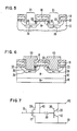
- FIGS. 1 through 6 illustrate a method for fabricating a power MOSFET structure
- FIG. 6 A cross-sectional view of the preferred embodiment of the semiconductor structure of this invention is shown in Figure 6.
- Figures 1 through 6 illustrate a method by which this power MOSFET structure may be manufactured.
- Figure 1 is a cross-sectional view of a semiconductor structure which may be fabricated using known processes.
- a lightly doped N- conductivity type epitaxial silicon layer 12 is deposited on the upper surface of a heavily doped N+ conductivity type silicon substrate 10.
- substrate 10 is a commercially available silicon substrate doped with antimony to an impurity concentration of 1019 atoms per cubic centimeter.
- Epitaxial layer 12 may be formed across the upper surface of substrate 10 using a suitable epitaxial reactor.
- epitaxial layer 12 is 10-50 microns thick and has a phosphorous impurity concentration of 1014 atoms per cubic centimeter.
- Substrate 10 will function as an electrical contact to epitaxial silicon 12 which will become the drain of the MOSFET.
- a relatively thin layer of silicon dioxide 15 is formed on the upper surface of epitaxial layer 12 .
- silicon dioxide 15 is 2000 Angstroms thick and is formed by heating the underlying structure to a temperature of 1000°C for 2 hours in oxygen. Silicon dioxide 15 will become the gate oxide of the MOSFET.
- a layer of polycrystalline silicon 18 is deposited, for example, using chemical vapor deposition.
- Polycrystalline silicon 18 will typically be on the order of 8000 Angstroms thick and is doped with arsenic to an impurity concentration of 1020 atoms per cubic centimeter.
- Polycrystalline silicon 18 may be doped while it is being deposited, or impurities may be introduced into it after deposition using known diffusion or ion implantation processes. Regions of the conductive polysilicon 18 will become the gate electrodes.
- a second layer of silicon dioxide 20 is formed, for example, by heating the underlying structure to a temperature of 1000°C for 30 minutes to create a layer 5000 Angstroms thick.
- a suitable mask (not shown) is deposited and patterned on the upper surface of silicon dioxide 20.
- the underlying layers of silicon dioxide 15 and 20 and polycrystalline silicon 18 are then removed from regions 22 and 24 as shown by Figure 2.
- this etching step is performed using plasma or reactive ion etching to thereby create relatively vertical cuts through the "sandwich" structure formed by layers 15, 18 and 20.
- Suitable etch gases for removing the silicon dioxide layers 15 and 20 include carbon tetrafluoride, while polycrystalline silicon 18 may be removed using carbon tetrachloride.
- the polycrystalline silicon 18 will be allowed to remain on the structure wherever gate electrodes for the power MOSFET structure are desired.
- the structure shown in Figure 2 is then oxidized by heating it to a temperature of 800°C for 2 hours to create the silicon dioxide 25 and 26 shown in regions 22 and 24 of Figure 3.
- the silicon dioxide forming on the side walls of the structure depicted will be approximately 3000 Angstroms thick, while that which forms directly on the surface of epitaxial silicon 12 will be approximately 8000 Angstroms thick.
- the silicon dioxide 25 on the side walls will serve to electrically isolate electrodes formed in regions 22 and 24 from the doped polycrystalline silicon gate electrodes 18.
- silicon dioxide 25 functions as a mask for the following etching step.
- the structure shown in Figure 3 is then etched to remove the silicon dioxide 26 from the bottom of the central portion of regions 22 and 24 as shown by Figure 4. This step may be accomplished using well-known plasma etching apparatus and carbon tetrafluoride etch gas.
- P and N conductivity type dopants are introduced into the upper surface of epitaxial layer 12 through the surfaces from which silicon dioxide 26 has been removed. These dopants form a P conductivity type region 30 and an N conductivity type region 33 in each opening.
- the dopants may be introduced using a variety of process operations. For example, in one embodiment the P conductivity type regions 30 are formed by ion implanting them below the surface of epitaxial layer 12. Then, using a lower implant energy, the N conductivity type regions 33 are fabricated closer to the upper surface of epitaxial material 12. The structure is then heated to a temperature of 1000°C for 2 hours to allow the implanted regions to diffuse into the configuration shown in Figure 4.
- the P type regions 30 will have a surface impurity concentration of 1017 boron atoms per cubic centi meter, while the N conductivity type regions 33 will have a surface impurity concentration of 1020 arsenic atoms per cubic centimeter.
- any silicon dioxide formed on the surface of epitaxial material 12 is removed, and the silicon itself etched in the manner shown in Figure 5.
- epitaxial silicon 12 will be etched using a plasma or reative ion process to create an opening which has substantially vertical sides, is 4000 Angstroms deep and extends at least all the way through N conductivity type regions 33.
- a well-known preferential chemical etch may be performed to create a V-groove structure.
- boron or other P conductivity type impurity may be implanted into the bottom of the openings 21 to form regions 36. Typically these regions will be doped to a concentration of 1020 atoms per cubic centimeter. If necessary the structure may then be heated to diffuse of the P type impurities 36 to form the structure shown in Figure 5.
- metal connections 40 are formed. These connections are typically formed by depositing a layer of aluminum across the entire upper surface of the structure and into openings 21. Using well-known masking and photolithographic techniques the metal layer is patterned into desired regions 40. Electrodes 40 function as contacts to the N conductivity type source regions and "short" source region 33 to gate region 30.
- the strongly doped N conductivity type wafer 10 is again shown in Figure 6 to illustrate the manner in which any electrical connection to the drain 12 of the power MOSFET is made. In a typical embodiment all of the gate electrodes 18 will be electrically connected to each other, as will all source electrodes 40. In this manner, a single chip will be cap able of controlling substantially more power than any single MOSFET therein.
- Figure 7 is a schematic diagram of an equivalent discrete circuit to the integrated circuit structure shown in Figure 6.
- the power MOS device is formed by gate 30, source 33, drain 12, and gate electrode 18.
- Metal contact 40 provides an electrical connection to source 33, while region 10 provides a connection to drain 12.
- the parasitic bipolar transistor formed by the structure shown in Figure 6 includes collector 12, emitter 33, and base 30.
- the strongly doped P type regions 36 beneath the gate and parasitic base region 30 reduce the base resistance of the parasitic bipolar transistor. Because the breakdown voltage of the MOS device is usually limited by the collector-emitter breakdown voltage of the parasitic bipolar device, (which in turn is proportional to the product of the collector-base breakdown voltage and the base resistance), the lowered base resistance increases the overall power MOS device breakdown voltage. The breakdown voltage may be further increased by improving the transconductance of the structure by increasing the packing density of the MOS devices formed on a single chip. The lowered gate capacitance per unit cell resulting from self-alignment of the gate and source, provides an increased ratio of transconductance to gate capacitance, thereby improving switching speed.
- Advantages of the structure depicted in Figure 6 include a significant reduction in the base resistance of the parasitic bipolar NPN transistor. This results from the self-aligned edge of the N+ diffusion 33 with the edge of the overlying polycrystalline silicon gate 18. The self-alignment increases the collector-emitter breakdown voltage of the parasitic bipolar transistor. Furthermore, by virtue of its compact layout, the structure shown in Figure 6 provides reduced source-drain resistance and increased transconductance over prior art structures.
Landscapes
- Metal-Oxide And Bipolar Metal-Oxide Semiconductor Integrated Circuits (AREA)
- Insulated Gate Type Field-Effect Transistor (AREA)
Priority Applications (1)
| Application Number | Priority Date | Filing Date | Title |
|---|---|---|---|
| EP89104187A EP0326187A3 (fr) | 1982-05-20 | 1983-05-17 | Structure MOSFET à puissance |
Applications Claiming Priority (3)
| Application Number | Priority Date | Filing Date | Title |
|---|---|---|---|
| US06/380,170 US4503598A (en) | 1982-05-20 | 1982-05-20 | Method of fabricating power MOSFET structure utilizing self-aligned diffusion and etching techniques |
| US380170 | 1982-05-20 | ||
| EP89104187A EP0326187A3 (fr) | 1982-05-20 | 1983-05-17 | Structure MOSFET à puissance |
Related Parent Applications (2)
| Application Number | Title | Priority Date | Filing Date |
|---|---|---|---|
| EP83400983.9 Division | 1983-05-17 | ||
| EP83400983A Division EP0094891B1 (fr) | 1982-05-20 | 1983-05-17 | Procédé pour la fabrication d'une structure verticale MOSFET de puissance |
Publications (2)
| Publication Number | Publication Date |
|---|---|
| EP0326187A2 true EP0326187A2 (fr) | 1989-08-02 |
| EP0326187A3 EP0326187A3 (fr) | 1989-09-27 |
Family
ID=26119943
Family Applications (1)
| Application Number | Title | Priority Date | Filing Date |
|---|---|---|---|
| EP89104187A Withdrawn EP0326187A3 (fr) | 1982-05-20 | 1983-05-17 | Structure MOSFET à puissance |
Country Status (1)
| Country | Link |
|---|---|
| EP (1) | EP0326187A3 (fr) |
Cited By (1)
| Publication number | Priority date | Publication date | Assignee | Title |
|---|---|---|---|---|
| WO2004066397A3 (fr) * | 2003-01-15 | 2004-10-28 | Advanced Power Technology | Conception et fabrication d'une diode a recuperation rapide robuste |
Family Cites Families (3)
| Publication number | Priority date | Publication date | Assignee | Title |
|---|---|---|---|---|
| NL184551C (nl) * | 1978-07-24 | 1989-08-16 | Philips Nv | Veldeffekttransistor met geisoleerde stuurelektrode. |
| DE3016749A1 (de) * | 1980-04-30 | 1981-11-05 | Siemens AG, 1000 Berlin und 8000 München | Kontakt fuer mis-halbleiterbauelement und verfahren zu seiner herstellung |
| DE3380136D1 (en) * | 1982-04-12 | 1989-08-03 | Gen Electric | Semiconductor device having a diffused region of reduced length and method of fabricating the same |
-
1983
- 1983-05-17 EP EP89104187A patent/EP0326187A3/fr not_active Withdrawn
Non-Patent Citations (1)
| Title |
|---|
| B. BALIGA: "Switching Lots of Watts at High Speed", IEEE SPECTRUM, December 1981 (1981-12-01), pages 42 - 48 |
Cited By (3)
| Publication number | Priority date | Publication date | Assignee | Title |
|---|---|---|---|---|
| WO2004066397A3 (fr) * | 2003-01-15 | 2004-10-28 | Advanced Power Technology | Conception et fabrication d'une diode a recuperation rapide robuste |
| US7169634B2 (en) | 2003-01-15 | 2007-01-30 | Advanced Power Technology, Inc. | Design and fabrication of rugged FRED |
| US7671410B2 (en) | 2003-01-15 | 2010-03-02 | Microsemi Corporation | Design and fabrication of rugged FRED, power MOSFET or IGBT |
Also Published As
| Publication number | Publication date |
|---|---|
| EP0326187A3 (fr) | 1989-09-27 |
Similar Documents
| Publication | Publication Date | Title |
|---|---|---|
| US4503598A (en) | Method of fabricating power MOSFET structure utilizing self-aligned diffusion and etching techniques | |
| US6566690B2 (en) | Single feature size MOS technology power device | |
| EP0110211B1 (fr) | Circuit intégré à transistors bipolaires et procédé de fabrication de celui-ci | |
| US5342797A (en) | Method for forming a vertical power MOSFET having doped oxide side wall spacers | |
| US4583106A (en) | Fabrication methods for high performance lateral bipolar transistors | |
| US4066473A (en) | Method of fabricating high-gain transistors | |
| US5663079A (en) | Method of making increased density MOS-gated semiconductor devices | |
| EP0137906A1 (fr) | Procédé de fabrication de transistors NPN verticaux et PNP latéraux dans le même corps semiconducteur | |
| KR100289474B1 (ko) | Dmos 트랜지스터를 제조하기 위한 방법 | |
| US4922315A (en) | Control gate lateral silicon-on-insulator bipolar transistor | |
| EP0001300B1 (fr) | Procédé de fabrication d'un dispositif semiconducteur du type LOCOS | |
| JP2748898B2 (ja) | 半導体装置およびその製造方法 | |
| US6030870A (en) | High density MOS technology power device | |
| EP0369336A2 (fr) | Procédé de fabrication des transistors bipolaires et CMOS sur un substrat commun | |
| CA1179786A (fr) | Transistor a structure laterale ayant une base auto-alignee et un contact de base et methode de fabrication | |
| KR970011641B1 (ko) | 반도체 장치 및 제조방법 | |
| KR0128339B1 (ko) | Cmos 기술을 이용하는 바이폴라 트랜지스터 제조방법 | |
| EP0451286B1 (fr) | Dispositif à circuit intégré | |
| EP0122004A2 (fr) | Construction d'un transistor bipolaire | |
| EP0159179A2 (fr) | Construction d'un transistor bipolaire | |
| JP2803548B2 (ja) | 半導体装置の製造方法 | |
| US4713355A (en) | Bipolar transistor construction | |
| JP2712359B2 (ja) | 半導体装置の製造方法 | |
| KR920003320B1 (ko) | 매우 작은 소오스 영역을 갖는 자기 정렬된 수직 이중 확산형 전력 mosfet의 제조방법 | |
| US5376563A (en) | Method of manufacturing an emitter base self alignment structure |
Legal Events
| Date | Code | Title | Description |
|---|---|---|---|
| PUAI | Public reference made under article 153(3) epc to a published international application that has entered the european phase |
Free format text: ORIGINAL CODE: 0009012 |
|
| AC | Divisional application: reference to earlier application |
Ref document number: 94891 Country of ref document: EP |
|
| AK | Designated contracting states |
Kind code of ref document: A2 Designated state(s): DE FR GB IT NL |
|
| PUAL | Search report despatched |
Free format text: ORIGINAL CODE: 0009013 |
|
| AK | Designated contracting states |
Kind code of ref document: A3 Designated state(s): DE FR GB IT NL |
|
| 17P | Request for examination filed |
Effective date: 19891130 |
|
| 17Q | First examination report despatched |
Effective date: 19920311 |
|
| STAA | Information on the status of an ep patent application or granted ep patent |
Free format text: STATUS: THE APPLICATION IS DEEMED TO BE WITHDRAWN |
|
| 18D | Application deemed to be withdrawn |
Effective date: 19920922 |