EP0326619B1 - Energieversorgung für mikrowellen-entladungslichtquelle - Google Patents
Energieversorgung für mikrowellen-entladungslichtquelle Download PDFInfo
- Publication number
- EP0326619B1 EP0326619B1 EP88906879A EP88906879A EP0326619B1 EP 0326619 B1 EP0326619 B1 EP 0326619B1 EP 88906879 A EP88906879 A EP 88906879A EP 88906879 A EP88906879 A EP 88906879A EP 0326619 B1 EP0326619 B1 EP 0326619B1
- Authority
- EP
- European Patent Office
- Prior art keywords
- voltage
- transformer
- magnetron
- circuit
- coupled
- Prior art date
- Legal status (The legal status is an assumption and is not a legal conclusion. Google has not performed a legal analysis and makes no representation as to the accuracy of the status listed.)
- Expired - Lifetime
Links
Images




Classifications
-
- H—ELECTRICITY
- H01—ELECTRIC ELEMENTS
- H01J—ELECTRIC DISCHARGE TUBES OR DISCHARGE LAMPS
- H01J65/00—Lamps without any electrode inside the vessel; Lamps with at least one main electrode outside the vessel
- H01J65/04—Lamps in which a gas filling is excited to luminesce by an external electromagnetic field or by external corpuscular radiation, e.g. for indicating plasma display panels
-
- H—ELECTRICITY
- H01—ELECTRIC ELEMENTS
- H01J—ELECTRIC DISCHARGE TUBES OR DISCHARGE LAMPS
- H01J65/00—Lamps without any electrode inside the vessel; Lamps with at least one main electrode outside the vessel
- H01J65/04—Lamps in which a gas filling is excited to luminesce by an external electromagnetic field or by external corpuscular radiation, e.g. for indicating plasma display panels
- H01J65/042—Lamps in which a gas filling is excited to luminesce by an external electromagnetic field or by external corpuscular radiation, e.g. for indicating plasma display panels by an external electromagnetic field
- H01J65/044—Lamps in which a gas filling is excited to luminesce by an external electromagnetic field or by external corpuscular radiation, e.g. for indicating plasma display panels by an external electromagnetic field the field being produced by a separate microwave unit
-
- H—ELECTRICITY
- H05—ELECTRIC TECHNIQUES NOT OTHERWISE PROVIDED FOR
- H05B—ELECTRIC HEATING; ELECTRIC LIGHT SOURCES NOT OTHERWISE PROVIDED FOR; CIRCUIT ARRANGEMENTS FOR ELECTRIC LIGHT SOURCES, IN GENERAL
- H05B41/00—Circuit arrangements or apparatus for igniting or operating discharge lamps
- H05B41/14—Circuit arrangements
- H05B41/24—Circuit arrangements in which the lamp is fed by high frequency AC, or with separate oscillator frequency
Definitions
- the present invention relates to a microwave generating system including a magnetron and a power supply circuit therefor, which is adapted to supply microwave energy to a microwave discharge light source, including an electrodeless bulb.
- Fig. la shows one of such microwave discharge light source apparatus disclosed in Japanese Laid-Open Patent Application 56-l26250;
- Fig. lb shows a modification thereof disclosed in Japanese Laid-Open Patent Application 57-5509l.
- a magnetron l having an antenna la is disposed at the end of a waveguide 2 having ventilating holes 2a which supplies the microwave generated by the magnetron l to a resonance cavity 3 through a microwave supply port 3a;
- the cavity 3 is formed by a paraboloidal wall 3b having a light reflecting rotationally symmetric inner surface and a metallic mesh 3c forming the front face of the cavity 3, which opaque to microwave but transparent to light.
- the apparatuses further comprise a fan 5 at the end wall of the housing 6 for cooling the magnetron l and the bulb 4.
- Microwave discharge light source apparatuses similar to those described above are also disclosed in U.S. Patent Nos. 4,498,029 and 4,673,846, both issued to Yoshizawa et al.
- the first of these U.S. Patents teach an apparatus in which the bulb is sufficiently small to act substantially as a point light source; the second teach an apparatus in which the wall surface of the microwave resonance cavity having the electrodeless bulb disposed therein is mostly constituted by a mesh, wherein the wires constituting the mesh are electrically connected each other without any contact resistance.
- a conventional power supply circuit for a magnetron is disclosed in Japanese Laid-Open Utility Model Application 56-l62899, or in the first of the above mentioned U.S. Patents, according to which a commercial voltage source at 50 to 60 Hz is coupled to a step-up transformer, and the resulting stepped-up high-voltage AC current is rectified by a full-wave rectifier circuit to obtain pulsing unidirectional current which is supplied to the magnetron.
- the rectification is effected by a full-wave rectifier circuit
- the resulting high voltage rectified current pulsates at l00 to l20 Hz; consequently, the magnetron generates a microwave pulsing at l00 to l20 Hz.
- the discharge in the bulb 4 is caused by the microwave pulsing at l00 to l20 Hz.
- the disadvantage of this type of conventional power supply circuit is as follows. First, as the commercial AC voltage of relatively low frequency, i.e., 50 to 60 Hz, is directly supplied to the primary winding of the step-up transformer to obtain a high voltage needed to supply the magnetron, the transformer should be provided with a heavy iron core; the weight of the transformer is equal to or greater than l0 kg when the input power to the magnetron is l.5 kW.
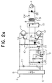
- Fig. 2a shows an inverter type power supply circuit for a magnetron taught in Japanese Patent Publication 60-l89889, wherein the magnetron l is supplied by the circuit as described in what follows.
- a rectifier circuit 8 is coupled across the lines of a commercial AC voltage source E; a pair of series-connected capacitors Cl and C2 are coupled across the output terminals of the rectifier circuit 8 to obtain a substantially constant voltage DC power.
- An oscillator circuit 9 which comprises a Zener diode Zn, a capacitor C3, a plurality of resistors, and an amplifier A, is coupled across the capacitor C2 to output a rectangular waveform signal having a frequency substantially higher than that of the commercial AC voltage source E to a control circuit l0 comprising a transistor Tl, a diode Dl, and a plurality of resistors; the frequency of the rectangular waveform signal of the oscillator circuit 9 is determined by the values of the resistors and the capacitor C3 thereof.
- the control circuit l0 controls the alternate switching actions of a switching circuit comprising the power transistors ll and l2 and the controlling transistors lla and l2a therefor.
- the circuit l0 alternately turns on and off the power transistors ll and l2 in response to the output signal of the oscillator circuit 9.
- a high frequency rectangular waveform AC current is supplied to the primary winding P of the transformer T through a filter circuit l3.
- the AC voltage induced in the secondary winding S of the transformer T is rectified by a voltage doubler rectifier circuit consisting of a capacitor C4 and a diode D2, and is supplied therefrom to the magnetron l.
- the inverter type power supply for a magnetron as described above also suffers disadvantages. Namely, as the magnetron l constitutes a non-linear load, the output power and current thereof and the inverter current supplied to the step-up transformer become unstable when the voltage level of the voltage source E fluctuates; the over-current resulting therefrom may destroy the power transistors ll and l2.
- Fig. 2b shows another inverter type power supply circuit for a magnetron taught in Japanese Laid-Open Patent Application 62-ll3395, wherein the magnetron l is supplied by the circuit as follows.
- a diode bridge rectifier circuit 8 comprising four diodes Do is coupled across the commercial AC voltage source E; a smoothing filter circuit 9 consisting of a capacitor Co is coupled across the output terminals of the rectifier circuit 8 to output a substantially constant DC voltage therefrom.
- the switching circuit l0 comprises switching transistors Ql and Q2 and diodes Dl and D2 for reverse currents coupled across the source and the drain thereof, respectively, the transistors Ql and Q2 being coupled across the negative output terminal of the filter circuit 9 and the terminals Pl and P2 of the primary winding P of the transformer T, respectively.
- the positive output terminal of the filter circuit 9 is coupled to the center tap 0 of the primary winding P of the transformer T.
- the gate terminals gl and g2 of the transistors Ql and Q2, respectively, is coupled to the center tap 0 of the primary winding P of the transformer T.
- the gate terminals gl and g2 of the transistors Ql and Q2, respectively, are coupled to the output terminals of a control circuit ll.
- the voltage doubler rectifier circuit l2 consisting of series-connected capacitor Cl and a diode D3 is coupled across the terminals Sl and S2 of the secondary winding S of the transformer T; the negative output terminal d of the rectifier circuit l2 is coupled to the cathode K of the magnetron l, which is heated by a filament current supplied thereto from a commercial AC voltage source through an electrically insulating transformer (not shown) and the lines h; the positive output terminal f of the rectifier circuit l2, on the other hand, is coupled to the anode A of the magnetron l through a resistor R, the terminals of the resistor R being coupled to the input terminals of the control circuit ll.
- the control circuit ll outputs pulses to the transistors Ql and Q2 at a varying frequency centered around a fixed frequency, to alternately turn on and off the transistors Ql and Q2.
- the current flows alternately from the center tap 0 to the terminal Pl and to the terminal P2 of the primary winding P of the transformer T to induce an AC voltage in the secondary winding S thereof, which is rectified by the rectifier circuit l2 and supplied therefrom to the magnetron l.
- the pulse signals of the control circuit ll at the fixed frequency are subjected to frequency modulation utilizing a modulating signal having a frequency which is lower than the frequency of the fixed frequency of the output pulse signals, to prevent flickering of the discharge in an electrodeless bulb such as those shown in Figs.
- the flickering of the discharge is caused by an acoustic resonance in the bulb due to the ripple or fluctuation of the microwave energy.
- the circuit ll varies the length of time during which the transistors Ql and Q2 are turned on, so that the output power of the magnetron is held constant irrespective of the fluctuation in the voltage source level; this can be effected by detecting the magnetron current by means of the voltage drop across the resistor R, thanks to the substantially constant voltage characteristic of the magnetron l.
- the inverter type power supply circuit for a magnetron described just above is small-sized and is effective to a certain degree to prevent the flickering of the discharge arc of the electrodeless discharge bulb, thanks to the adoption of the high frequency inverter in the circuit.
- the flickering of the discharge arc may persist even in the apparatuses supplied by the circuit, depending on the kind and amount of the material encapsulated in the bulb and on the microwave energy level radiated into the bulb: the flickering of the arc is particularly manifest when a metal halide compound such as sodium iodide is ancapsulated in the bulb in addition to mercury and a starter rare gas, or when the microwave energy supplied to the bulb is at a high level.
- the controlling circuit ll thereof has a complicated structure, because the pulse signals thereof are subjected to frequency modulation and the length of the turning-on time of the switching is varied to maintain the output power of the mangetron l at a constant level.
- Japanese Laid-Open Patent Application 62-290098 teaches a microwave discharge light source apparatus including an inverter type power supply circuit for the magnetron, wherein the inverter frequency is set at a few tens kHz, for example, thereby maintaining parameters of the plasma in the bulb at a substantially constant level to prevent the flickering of the discharge in the bulb.
- an object of the present invention is to provide a power supply circuit including a magnetron adapted to supply microwave energy to a microwave discharge light source apparatus including an electrodeless discharge bulb, wherein the circuit is small in size and light in weight; more particularly, an object of the present invention is to reduce the size and weight of the step-up transformer comprised in the circuit.
- Another object of the present invention is to provide such power supply circuit including a magnetron which supplies microwave energy that is capable of sustaining stable discharge in the electrodeless bulb of the light source apparatus; namely, it is an object of the present invention to provide a power supply circuit which does not cause flickering in the discharge in the bulb and which is capable of sustaining the discharge in the bulb without any fear of extinguishment.
- a circuit system adapted to supply microwave energy to a microwave discharge light source apparatus including an electrodeless discharge bulb, comprising: first rectifier means, adapted to be coupled to an AC voltage source of a relatively low voltage and frequency, for outputting a rectified voltage of a relatively low voltage; filter means, coupled to said first rectifier means, for smoothing said rectified voltage outputted from said first rectifier means, and for outputting a smoothed rectified voltage; inverter means, coupled to said filter means, for converting said smoothed rectified voltage outputted from said filter means to an AC voltage of a relatively high frequency having a waveform of alternating pulses; a step-up transformer having a primary winding coupled to an output of said inverter means, a secondary winding of the step-up transformer outputting an AC voltage of said relative high frequency and of a relatively high voltage; second filter means, coupled to said second winding of said step-up transformer, for rectifying said AC voltage, of the relative high frequency and the relative high voltage outputted from said secondary wind
- the inductance means reduces high frequency components in the current flowing through the primary or the secondary winding of the step-up transformer. Thus, stable operation of the inverter is ensured.
- the power supply circuit for the magnetron l comprises a diode bridge full-wave rectifier circuit 2, the input terminals of which are coupled across a commercially available AC voltage source E, typically on the order of l00 to 220 volts RMS at 50 to 60 Hz.
- a voltage divider consisting of a pair of resistors Rl and R2 connected in series is coupled across the output terminals of the rectifier circuit 2.
- a capacitor Cl constituting a smoothing filter circuit is coupled across the output terminals of the rectifier circuit 2 to supply a substantially constant DC voltage therefrom.
- the input terminals of the inverter switching circuit comprising four MOSFETs (metal oxide semiconductor field effect transistors) Ql through Q4 connected in bridge circuit relationship are coupled across the output terminals of the filter circuit, the capacitor Cl; the output terminals of the switching circuit is coupled across the primary or input winding P of the step-up transformer T having a step-up ratio of l to n, a reactor L being inserted in series with the primary winding P.
- the inverter switching circuit further comprises four diodes Dl through D4 for reverse currents, which are coupled across the source and the drain terminal of the MOSFETs Ql through Q4, respectively, the gate terminals of the MOSFETs being coupled to the output terminals of the PWM (pulse width modulation) control circuit 3.
- a voltage doubler half-wave rectifier circuit consisting of a capacitor C2 and a diode D5 connected in series is coupled across the secondary or output winding S of the transformer T; the output terminals of the rectifier circuit, i.e., the terminals across the diode D5, are coupled across the cathode K and the anode An of the magnetron l to supply a pulsating DC current I Mg thereto.
- the output terminals of a current detector 4 for detecting the current flowing through the secondary winding S of the transformer T are coupled to the PWM control circuit 3 to output a voltage Vf corresponding to the current flowing through the secondary winding S.
- the control circuit 3 comprises a half-wave rectifier 3a rectifying the output Vf of the current detector 4, a smoothing filter 3b coupled to the output of the rectifier 3a to output a smoothed voltage Vf corresponding to the mean value of the voltage Vf;
- the duration T ON of the positive voltage Vl i.e., the pulse width thereof corresponds to the pulse width of the gate signal outputted from the driver 3i and that of the signal Vw outputted from the PWM modulator 3h of the control circuit 3; the height of the pulse Vl is substantially equal to the output voltage Vo of the filtering capacitor Cl. Due to the inductance of the reactor L connected in series with the primary winding P of the transformer T, the current i l flowing through the primary winding P in the direction shown by the arrow in Fig. 3a increases gradually from zero to a maximum during the time in which the voltage Vl is maintained at the positive level, as shown in Fig.
- the current i l in the primary winding P of the transformer persists during a short time Tx, due to the existance of the inductance of the reactor L connected in series with the primary winding P.
- the current i l flows through the diodes D2 and D3 to charge the capacitor Cl.
- the current induced in the secondary winding S of the transformer during this positive half-cycle Tp of the inverter has a polarity corresponding to the conducting direction of the diode D5; thus, no currents i Mg flows through the magnetron l and the voltage V2 across the cathode K and the anode An of the magnetron l is equal to zero, as shown in Fig. 4 (c) and (d), the capacitor C2 being charged by the current induced in the secondary winding S during the positive half-cycle Tp.
- the voltage V2 applied across the mangetron l increases gradually during the time T ON in which the MOSFETs Q2 and Q3 are turned on and the output voltage Vl of the switching circuit is kept at the negative level, due to the gradual decrease of the voltage developed across the reactor L during the same time period T ON .
- the current i Mg flowing through the magnetron l increases gradually from Zero to a maximum, as shown in Fig. 4(d) during the time T ON , due to the current-voltage characteristic of the magnetron l. Namely, as shown in Fig.
- the voltage V2 across the magnetron l plotted along the ordinate is at a finite voltage level Vz when the magnetron current i Mg plotted along the abscissa begins to flow through the magnetron l.
- the output power of the magnetron l is held at a constant level by the modulation of the pulse width T ON of the gate signals applied to the MOSFETs Ql through Q4 from the control circuit 3. Detailed explanation thereof is as follows.
- the output power P OUT of the magnetron l is approximately given by the product of the mean value of the magnetron current i Mg shown in Fig. 4(d) and the magnetron voltage V2, because the rise ⁇ Vz in the voltage V2 is small compared to the magnitude of the cut-off voltage Vz, as shown in Fig. 5, when the magnetron l is operated within the rated current and voltage range.
- P OUT is approximated as follows: P OUT ⁇ f ⁇ V z / n ( ⁇ 2 + ⁇ 2 )L ⁇ (2V o - V z /n) ⁇ l+a l-a ⁇ b (l+b), wherein, the meanings of the symbols are as follows :
- the value X is proportional to the pulse width T ON when the inductance L of the reactor L is large enough; for example, in the case where the frequency f of the inverter is around l00 kHz and the pulse width T ON is limited within the range from about 4 to 5 microseconds, the magnetron peak current i Mg max can be represented by a linear equation if the value of L is selected at 8 miceohenries at which the value of X is approximately proportional to the pulse width T ON ; namely, i Mg max is approximated by: i Mg max ⁇ K ⁇ (2Vo - V2/n) ⁇ T ON , wherein K is the proportionality constant determined by the relationship between X and T ON .
- Vo V DC + ⁇ V
- V DC represents the pure DC, i.e., constant, component of the voltage Vo
- ⁇ V represents the AC component, i.e., variation, of the voltage Vo.
- the pulse width T ON is approximately expressed as follows: T ON ⁇ K2 - K3 ⁇ ⁇ V, wherein K2 and K3 are constants determined by the values of Kl, Vo, V DC , and n.
- the peak current i Mg max of the magnetron l can be maintained at a constant level irrespective of the variation ⁇ V in the smoothed DC voltage Vo outputted from the filtering capacitor Cl.
- the magnetron peak current i Mg max is held substantially constant even when the AC line voltage source E fluctuates. In other words, the inverter current flowing through the MOSFETs Ql through Q4 is stabilized, thereby eliminating the danger of failures thereof.
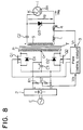
- FIG. 8 and 9 of the drawings a second and a third embodiment according to the present invention having a push-pull type inverter switching circuit are described.
- the source and the drain terminal of the MOSFETs Ql and Q2 are coupled across the negative terminal of the capacitor Cl and the terminals of the primary winding P of the step-up transformer T, respectively, the positive output terminal of the capacitor Cl being coupled to the center tap 0 of the primary winding P of the transformer T.
- the reactor L having a function corresponding to that of the reactor L of the first embodiment is inserted in series with the secondary winding S of the transformer T, the capacitor C2 and the diode D3 being coupled in series with the secondary winding S and the reactor L to form a rectifier circuit corresponding to the rectifier current consisting of the capacitor C2 and the diode D5, as in the case of the first embodiment.
- the primary winding of the transformer T is devided into two portions Pl and P2; a mutual inductance M having a pair of magnetically coupled coils Ml and M2 is coupled across the terminals Ol and O2 without dot marks in the figure, the mutual inductance M effecting a function corresponding to that of the reactor L of the first embodiment.
- the MOSFETs Ql and Q2 are coupled across the negative terminal of the capacitor Cl and the dotted terminals O3 and O4 of the windings Pl and P2, respectively; the positive terminal of the capacitor Cl is coupled to the terminal between the two coils Ml and M2 of the mutual inductance M.
- the circuit coupled to the secondary winding S of this third embodiment is similar to that of the first embodiment.
- the voltage devider consisting of the series connected resistors Rl and R2 outputs a voltage Vin corresponding to the output voltage Vo of the capacitor Cl to the PWM control circuit 3;
- the current detector 4 detects the current flowing through the secondary winding S of the transformer T and output a voltage Vf corresponding thereto to the control circuit 3.
- the control circuit 3, which has a structure and an operation similar to those of the control circuit 3 of the first embodiment, outputs gate signals alternately to the MOSFETs Ql and Q2, and alternately turns them on and off, modulating the pulse width thereof.
- the induced voltage in the secondary winding S of the transformer T has a polarity agreeing with that of the diode D3; consequently, the induced current in the secondary winding S charges the capacitor C2 during the positive half-cycle.
- the MOSFET Q2 is turned on, while the MOSFET Q1 is turned off; thus, the polarity of the induced voltage in the secondary winding S is reversed, and is applied across the magnetron 1 together with the voltage developed across the capacitor C2.
- the resulting voltage V2 causing current i Mg to flow from the anode An to the cathode K of the Magnetron 1.
- the inverter switching circuit may be constituted by a half bridge circuit or monolithic forward circuit instead of full bridge circuit or push-pull circuit.
- the switching circuit may comprise, instead of MOSFETs utilized in the embodiments described above, power transistors SIT or GTO, SI thyristors, or magnetic amplifiers.
- the inductance L in the first and the second embodiment may be constituted by a leakage inductance of the step-up transformer, ie, the self-inductances of the primary and the secondary winding thereof.
Landscapes
- Physics & Mathematics (AREA)
- Engineering & Computer Science (AREA)
- Plasma & Fusion (AREA)
- Electromagnetism (AREA)
- Control Of High-Frequency Heating Circuits (AREA)
- Inverter Devices (AREA)
- Circuit Arrangements For Discharge Lamps (AREA)
- Discharge-Lamp Control Circuits And Pulse- Feed Circuits (AREA)
- Discharge Lamps And Accessories Thereof (AREA)
Claims (12)
- l. Schaltungssystem, das ausgebildet ist, um einer Lichtquelleneinrichtung vom Mikrowellenentladungstyp, die eine elektrodenlose Entladungslampe (4) hat, Mikrowellenenergie zuzuführen, wobei das Schaltungssystem folgendes aufweist:
eine erste Gleichrichtereinrichtung (2), die ausgebildet ist, um mit einer Wechselspannungsquelle (E) relativ niedriger Spannung und Frequenz gekoppelt zu werden, um eine gleichgerichtete Spannung (Vo) relativ niedriger Spannung zu liefern;
eine Filtereinrichtung (Cl), die mit der ersten Gleichrichtereinrichtung (2) gekoppelt ist, um die von der ersten Gleichrichtereinrichtung gelieferte gleichgerichtete Spannung zu glätten und eine geglättete gleichgerichtete Spannung zu liefern;
eine Wechselrichtereinrichtung (Ql bis Q4), die mit der Filtereinrichtung (Cl) gekoppelt ist, um die von der Filtereinrichtung gelieferte geglättete gleichgerichtete Spannung in eine Wechselspannung (Vl) relativ hoher Frequenz mit einer Wellenform von Wechselstromimpulsen umzuwandeln;
einen Aufwärtstransformator (T) mit einer Primärwicklung (P), die mit einem Ausgang der Wechselrichtereinrichtung gekoppelt ist, wobei eine Sekundärwicklung (S) des Aufwärtstransformators eine Wechselspannung relativ hoher Frequenz und relativ hoher Spannung liefert;
eine zweite Filtereinrichtung (C2, D5), die mit der Sekundärwicklung (S) des Aufwärtstransformators (T) gekoppelt ist, um die von der Sekundärwicklung gelieferte Wechselspannung der relativ hohen Frequenz und relativ hohen Spannung in eine gleichgerichtete Spannung (V₂) relativ hoher Spannung gleichzurichten; und
ein Magnetron (l), das mit der zweiten Gleichrichtereinrichtung (C₂, D₅) gekoppelt ist, um mit der von der zweiten Gleichrichtereinrichtung gelieferten gleichgerichteten Spannung (V₂) der relativ hohen Spannung versorgt und davon betrieben zu werden; und
eine Impulsdauermodulations-Steuereinrichtung (3), um die Impulsdauer der Impulse der von der Gleichrichtereinrichtung gelieferten Wechselspannung zu modulieren;
gekennzeichnet durch
eine Induktivitätseinrichtung (L) mit einem Induktivitätswert, der wirksam ist, um eine im wesentlichen lineare Beziehung zwischen der EIN-Dauer der Impulse der Wechselrichtereinrichtung und dem maximalen Magnetronstrom zu realisieren, wobei die Induktivitätseinrichtung (L) betriebsmäßig mit dem Aufwärtstransformator (T) gekoppelt ist, um eine rasche Änderung eines Pegels eines durch eine Wicklung des Aufwärtstransformators fließenden Stroms zu unterdrücken. - 2. Schaltungssystem nach Anspruch l, wobei die Wechselrichtereinrichtung einen Schaltkreis aufweist, der vier Transistoren (Ql bis Q4) hat, die in Vollbrückenschaltungsbeziehung elektrisch verbunden sind.
- 3. Schaltungssystem nach Anspruch l, wobei die Wechselrichtereinrichtung einen Schaltkreis aufweist, der ein Paar von Transistoren (Ql, Q2) hat, die in Gegentaktschaltungsbeziehung elektrisch verbunden sind.
- 4. Schaltungssystem nach Anspruch l oder 2, wobei die Induktivitätseinrichtung eine Induktivität (L) aufweist, die mit der Primärwicklung (P) des Aufwärtstransformators (T) elektrisch in Reihe geschaltet ist.
- 5. Schaltungssystem nach Anspruch l oder 3, wobei die Induktivitätseinrichtung eine Induktivität (L) aufweist, die mit der Sekundärwicklung (S) des Aufwärtstransformators (T) elektrisch in Reihe geschaltet ist.
- 6. Schaltungssystem nach einem der Ansprüche l bis 3, wobei die Induktivitätseinrichtung eine Streuinduktivität des Aufwärtstransformators aufweist.
- 7. Schaltungssystem nach Anspruch l oder 3, wobei die Primärwicklung (P) des Aufwärtstransformators (T) einen ersten (Pl) und einen zweiten (P2) Wicklungsteil aufweist und die Induktivitätseinrichtung eine gegenseitige Induktivität (M) aufweist, die elektrisch zwischen den ersten und den zweiten Wicklungsteil der Primärwicklung in Reihenschaltungsbeziehung geschaltet ist.
- 8. Schaltungssystem nach Anspruch l, wobei die Impulsdauermodulations-Steuereinrichtung (3) aufweist: einen Stromdetektor (4), um einen Strompegel eines Stroms zu detektieren, der durch das Magnetron fließt, und eine Einrichtung (3i), um die Impulsdauer der von der Wechselrichtereinrichtung gelieferten Wechselspannung aufgrund des von dem Detektor detektieren Strompegels des durch das Magnetron (l) fließenden Stroms zu ändern und dadurch eine Ausgangsleistung des Magnetrons auf einem vorbestimmten Pegel zu halten.
- 9. Schaltungssystem nach Anspruch 8, wobei der vorbestimmte Pegel veränderbar ist.
- 10. Schaltungssystem nach Anspruch l, wobei die erste Gleichrichtereinrichtung (2) vier Dioden aufweist, die in Brückenschaltungsbeziehung elektrisch verbunden sind.
- 11. Schaltungssystem nach Anspruch l oder l0, wobei die Filtereinrichtung einen Kondensator (Cl) aufweist, der Ausgangsanschlüssen der Gleichrichtereinrichtung (2) elektrisch parallelgeschaltet ist.
- 12. Schaltungssystem nach Anspruch l, wobei die zweite Gleichrichtereinrichtung eine Diode (D5) und einen Kondensator (C2) in Reihenschaltung aufweist, die parallel zu den Anschlüssen der Sekundärwicklung (S) des Aufwärtstransformators geschaltet ist.
Priority Applications (2)
| Application Number | Priority Date | Filing Date | Title |
|---|---|---|---|
| EP91202578A EP0474316B1 (de) | 1987-07-28 | 1988-07-27 | Leistungsversorgung für eine, durch Mikrowellen betriebene, Entladungslampe |
| EP91202577A EP0474315B1 (de) | 1987-07-28 | 1988-07-27 | Apparat mit Mikrowellen-Entladungs-Lichtquelle |
Applications Claiming Priority (2)
| Application Number | Priority Date | Filing Date | Title |
|---|---|---|---|
| JP62188256A JPH07111918B2 (ja) | 1987-07-28 | 1987-07-28 | マイクロ波放電光源装置 |
| JP188256/87 | 1987-07-28 |
Related Child Applications (3)
| Application Number | Title | Priority Date | Filing Date |
|---|---|---|---|
| EP91202577A Division EP0474315B1 (de) | 1987-07-28 | 1988-07-27 | Apparat mit Mikrowellen-Entladungs-Lichtquelle |
| EP91202577.2 Division-Into | 1991-10-03 | ||
| EP91202578.0 Division-Into | 1991-10-03 |
Publications (2)
| Publication Number | Publication Date |
|---|---|
| EP0326619A1 EP0326619A1 (de) | 1989-08-09 |
| EP0326619B1 true EP0326619B1 (de) | 1992-09-16 |
Family
ID=16220502
Family Applications (3)
| Application Number | Title | Priority Date | Filing Date |
|---|---|---|---|
| EP88906879A Expired - Lifetime EP0326619B1 (de) | 1987-07-28 | 1988-07-27 | Energieversorgung für mikrowellen-entladungslichtquelle |
| EP91202578A Expired - Lifetime EP0474316B1 (de) | 1987-07-28 | 1988-07-27 | Leistungsversorgung für eine, durch Mikrowellen betriebene, Entladungslampe |
| EP91202577A Revoked EP0474315B1 (de) | 1987-07-28 | 1988-07-27 | Apparat mit Mikrowellen-Entladungs-Lichtquelle |
Family Applications After (2)
| Application Number | Title | Priority Date | Filing Date |
|---|---|---|---|
| EP91202578A Expired - Lifetime EP0474316B1 (de) | 1987-07-28 | 1988-07-27 | Leistungsversorgung für eine, durch Mikrowellen betriebene, Entladungslampe |
| EP91202577A Revoked EP0474315B1 (de) | 1987-07-28 | 1988-07-27 | Apparat mit Mikrowellen-Entladungs-Lichtquelle |
Country Status (7)
| Country | Link |
|---|---|
| US (3) | US4988922A (de) |
| EP (3) | EP0326619B1 (de) |
| JP (1) | JPH07111918B2 (de) |
| KR (1) | KR920001875B1 (de) |
| CA (1) | CA1304773C (de) |
| DE (3) | DE3853169T2 (de) |
| WO (1) | WO1989001234A1 (de) |
Families Citing this family (52)
| Publication number | Priority date | Publication date | Assignee | Title |
|---|---|---|---|---|
| JPH07111918B2 (ja) | 1987-07-28 | 1995-11-29 | 三菱電機株式会社 | マイクロ波放電光源装置 |
| JPH0482191A (ja) * | 1990-07-25 | 1992-03-16 | Matsushita Electric Ind Co Ltd | 高周波加熱装置 |
| KR940008029B1 (ko) * | 1991-06-28 | 1994-08-31 | 삼성전자 주식회사 | 마그네트론 구동용 전원장치 |
| DE9305236U1 (de) * | 1992-04-11 | 1993-09-02 | Segor GmbH & Co KG, 55765 Birkenfeld | Wechselverkehrszeichengeber |
| US5558806A (en) * | 1992-07-23 | 1996-09-24 | Osi Specialties, Inc. | Surfactant blend of a polyalkleneoxide polysiloxane and an organic compound having a short chain hydrophobic moiety |
| DE4238198A1 (de) * | 1992-11-12 | 1994-05-19 | Abb Patent Gmbh | Schaltungsanordnung für ein Schaltnetzteil |
| US6075331A (en) * | 1993-03-18 | 2000-06-13 | Imra America, Inc. | Systems and methods for managing energy of electric power supply systems |
| US5438242A (en) * | 1993-06-24 | 1995-08-01 | Fusion Systems Corporation | Apparatus for controlling the brightness of a magnetron-excited lamp |
| US5495209A (en) * | 1995-04-14 | 1996-02-27 | Hughes Missile Systems Company | Switched-inverter modulator for producing modulated high voltage pulses |
| US5777867A (en) * | 1995-09-14 | 1998-07-07 | Suitomo Electric Industries, Ltd. | Electric discharge method and apparatus |
| US5838114A (en) * | 1996-03-08 | 1998-11-17 | Fusion Systems Corporation | Plural ferro-resonant power supplies for powering a magnetron where the aray lies in these power supplies being independent from each other and not utilizing any common components |
| US5909086A (en) * | 1996-09-24 | 1999-06-01 | Jump Technologies Limited | Plasma generator for generating unipolar plasma |
| DE19801711A1 (de) * | 1998-01-17 | 1999-07-22 | Aixcon Elektrotechnik Gmbh | Magnetronstromversorgung |
| WO2000040056A1 (en) * | 1998-12-23 | 2000-07-06 | United Automation Limited | Magnetron controller with transformer controlling the inrush current |
| US6958063B1 (en) | 1999-04-22 | 2005-10-25 | Soring Gmbh Medizintechnik | Plasma generator for radio frequency surgery |
| JP3087752B1 (ja) * | 1999-06-15 | 2000-09-11 | 松下電器産業株式会社 | マグネトロンの駆動電源 |
| US7126450B2 (en) * | 1999-06-21 | 2006-10-24 | Access Business Group International Llc | Inductively powered apparatus |
| KR100766534B1 (ko) * | 2000-09-27 | 2007-10-15 | 마쯔시다덴기산교 가부시키가이샤 | 마그네트론 구동용 전원 |
| KR100407045B1 (ko) * | 2001-03-12 | 2003-11-28 | 삼성전자주식회사 | 고출력 전환수단을 구비한 전자레인지 |
| JP2002367768A (ja) * | 2001-06-04 | 2002-12-20 | Matsushita Electric Ind Co Ltd | マグネトロン駆動用電源 |
| GB0120993D0 (en) * | 2001-08-30 | 2001-10-24 | Quay Technologies | Pulsed UV light source |
| DE10149827A1 (de) * | 2001-10-09 | 2003-04-30 | Siemens Ag | Stabilisierungsschaltung |
| KR100419204B1 (ko) * | 2001-12-24 | 2004-02-21 | 삼성전자주식회사 | 전자렌지 |
| KR100438619B1 (ko) * | 2002-01-25 | 2004-07-02 | 엘지전자 주식회사 | 마이크로 웨이브 조명장치 및 방법 |
| US6963267B2 (en) * | 2002-03-15 | 2005-11-08 | Wayne-Dalton Corporation | Operator for a movable barrier and method of use |
| KR20030079546A (ko) * | 2002-04-04 | 2003-10-10 | 엘지전자 주식회사 | 전자레인지 구동회로 |
| JP2003339164A (ja) | 2002-05-22 | 2003-11-28 | Hitachi Industrial Equipment Systems Co Ltd | スイッチング電源回路、及びインバータ装置 |
| TW569651B (en) * | 2002-07-05 | 2004-01-01 | Delta Electronics Inc | High-frequency heating device |
| WO2004095886A1 (en) * | 2003-04-22 | 2004-11-04 | Matsushita Electric Industrial Co. Ltd. | High-frequency dielectric heating device and printed board with thermistor |
| KR100565343B1 (ko) * | 2003-08-14 | 2006-03-30 | 엘지전자 주식회사 | 무전극 조명기기의 구동장치 |
| KR100575665B1 (ko) | 2003-09-25 | 2006-05-03 | 엘지전자 주식회사 | 마이크로웨이브 조명장치 |
| JP4204505B2 (ja) * | 2004-03-31 | 2009-01-07 | 日本高周波株式会社 | マグネトロン発振装置 |
| US7109669B2 (en) * | 2004-04-08 | 2006-09-19 | Nordson Corporation | Microwave lamp power supply that can withstand failure in high voltage circuit |
| GB2415785B (en) * | 2004-07-02 | 2006-11-22 | Ohm Ltd | Electromagnetic surveying |
| KR100677277B1 (ko) * | 2005-05-11 | 2007-02-02 | 엘지전자 주식회사 | 무전극 램프 시스템 |
| US20070096657A1 (en) * | 2005-10-31 | 2007-05-03 | Lg Electronics Inc. | Plasma lighting system and driving control method thereof |
| US9378930B2 (en) * | 2009-03-05 | 2016-06-28 | Applied Materials, Inc. | Inductively coupled plasma reactor having RF phase control and methods of use thereof |
| KR101106409B1 (ko) * | 2009-07-10 | 2012-01-17 | 엘지전자 주식회사 | 무전극 조명기기 및 제어 방법 |
| JP2011060566A (ja) * | 2009-09-10 | 2011-03-24 | Panasonic Corp | 高周波加熱装置 |
| WO2011050306A1 (en) * | 2009-10-23 | 2011-04-28 | Kaonetics Technologies, Inc. | Device, system and method for generating electromagnetic wave forms, subatomic particles, substantially charge-less particles, and/or magnetic waves with substantially no electric field |
| EP2827360A1 (de) * | 2010-03-22 | 2015-01-21 | Robe Lighting, Inc | Automatisierte Leuchte mit Plasmalichtquelle |
| US8269190B2 (en) | 2010-09-10 | 2012-09-18 | Severn Trent Water Purification, Inc. | Method and system for achieving optimal UV water disinfection |
| JP5776496B2 (ja) * | 2011-10-31 | 2015-09-09 | 富士電機株式会社 | 電力変換装置 |
| DE102012007450B4 (de) * | 2012-04-13 | 2024-02-22 | Tridonic Gmbh & Co Kg | Wandler für ein Leuchtmittel, LED-Konverter und Verfahren zum Betreiben eines LLC-Resonanzwandlers |
| WO2014010226A1 (ja) * | 2012-07-09 | 2014-01-16 | 東芝ホクト電子株式会社 | プラズマ発光装置とそれに用いる電磁波発生器 |
| US9316038B2 (en) | 2013-03-15 | 2016-04-19 | Overhead Door Corporation | Factory programming of paired authorization codes in wireless transmitter and door operator |
| JP6793192B2 (ja) * | 2016-06-27 | 2020-12-02 | シャープ株式会社 | 高周波加熱装置 |
| US11432732B2 (en) | 2016-06-28 | 2022-09-06 | Chiscan Holdings, Llc | System and method of measuring millimeter wave of cold atmospheric pressure plasma |
| US11166762B2 (en) * | 2016-06-28 | 2021-11-09 | Chiscan Holdings, L.L.C. | Non-thermal plasma generator for detection and treatment of maladies |
| US10230296B2 (en) * | 2016-09-21 | 2019-03-12 | Express Imaging Systems, Llc | Output ripple reduction for power converters |
| CA3077229C (en) * | 2017-11-03 | 2023-08-01 | Heraeus Noblelight America Llc | Ultraviolet lamp systems and methods of operating and configuring the same |
| CN114025664A (zh) | 2019-05-06 | 2022-02-08 | 智像控股有限责任公司 | 使用非热等离子体阵列的推定的能量场分析 |
Family Cites Families (33)
| Publication number | Priority date | Publication date | Assignee | Title |
|---|---|---|---|---|
| US4005370A (en) * | 1974-09-10 | 1977-01-25 | Matsushita Electric Industrial Co., Ltd. | Power supply means for magnetron |
| US3973165A (en) * | 1975-04-28 | 1976-08-03 | Litton Systems, Inc. | Power supply for a microwave magnetron |
| GB1542662A (en) * | 1975-09-12 | 1979-03-21 | Matsushita Electric Industrial Co Ltd | Power supply |
| US4356431A (en) * | 1978-02-21 | 1982-10-26 | Advance Transformer Company | Magnetron energizing circuit |
| DE3008143C2 (de) * | 1980-03-04 | 1982-04-08 | Ruwel-Werke Spezialfabrik für Leiterplatten GmbH, 4170 Geldern | Verfahren zum Herstellen von gedruckten Leiterplatten mit Lochungen, deren Wandungen metallisiert sind |
| JPS56126250A (en) * | 1980-03-10 | 1981-10-03 | Mitsubishi Electric Corp | Light source device of micro wave discharge |
| JPH0115118Y2 (de) | 1980-05-07 | 1989-05-08 | ||
| JPS6057676B2 (ja) * | 1980-09-19 | 1985-12-16 | 三菱電機株式会社 | マイクロ波放電光源用電源装置 |
| US4463286A (en) * | 1981-02-04 | 1984-07-31 | North American Philips Lighting Corporation | Lightweight electronic ballast for fluorescent lamps |
| US4532456A (en) * | 1982-07-12 | 1985-07-30 | Gte Products Corporation | Output circuit for an electronic ballast system |
| US4484108A (en) * | 1982-08-02 | 1984-11-20 | North American Philips Corporation | High frequency ballast-ignition system for discharge lamps |
| US4593167A (en) * | 1982-08-02 | 1986-06-03 | Nilssen Ole K | Electronic microwave oven power supply |
| JPS59114795A (ja) * | 1982-12-21 | 1984-07-02 | 三菱電機株式会社 | マイクロ波放電光源装置用電源装置 |
| US4585974A (en) * | 1983-01-03 | 1986-04-29 | North American Philips Corporation | Varible frequency current control device for discharge lamps |
| JPS59203399A (ja) * | 1983-05-06 | 1984-11-17 | 三菱電機株式会社 | マイクロ波放電光源装置 |
| US4609850A (en) * | 1983-06-01 | 1986-09-02 | Intent Patents A.G. | Current driven gain controlled electronic ballast system |
| US4673846A (en) * | 1984-03-02 | 1987-06-16 | Mitsubishi Denki Kabushiki Kaisha | Microwave discharge light source apparatus |
| JPS60189889A (ja) * | 1984-03-12 | 1985-09-27 | 松下電器産業株式会社 | 高周波加熱装置 |
| US4544863A (en) * | 1984-03-22 | 1985-10-01 | Ken Hashimoto | Power supply apparatus for fluorescent lamp |
| GB8419373D0 (en) * | 1984-07-30 | 1984-09-05 | Westinghouse Brake & Signal | Power control circuit |
| US4885506A (en) * | 1984-12-06 | 1989-12-05 | Nilssen Ole K | Electronic magnetron power supply |
| US4644459A (en) * | 1985-02-04 | 1987-02-17 | Nilssen Ole K | Electronic inverter having magnitude-controllable output |
| JPS61185887A (ja) * | 1985-02-13 | 1986-08-19 | 株式会社デンソー | 自動車用電磁波加熱装置 |
| KR900004338B1 (ko) * | 1985-03-25 | 1990-06-22 | 가부시기가이샤 히다찌 세이사구쇼 | 마그네트론 필터장치 |
| JPS61259488A (ja) * | 1985-05-14 | 1986-11-17 | 松下電器産業株式会社 | 高周波加熱装置 |
| JPS6273598A (ja) * | 1985-09-27 | 1987-04-04 | 株式会社日立製作所 | マイクロ波光源 |
| JPS6290899A (ja) * | 1985-10-16 | 1987-04-25 | 三菱電機株式会社 | マイクロ波放電光源装置用電源装置 |
| NL8503008A (nl) * | 1985-11-04 | 1987-06-01 | Philips Nv | Gelijkstroom-wisselstroomomzetter voor het ontsteken en voeden van een ontladingslamp. |
| JPS62113395A (ja) * | 1985-11-11 | 1987-05-25 | 三菱電機株式会社 | マイクロ波光源装置用電源装置 |
| US4700112A (en) * | 1986-07-08 | 1987-10-13 | Chang Ming J | Fluorescent lamp lighting circuit |
| JPS62290098A (ja) * | 1987-04-24 | 1987-12-16 | 三菱電機株式会社 | マイクロ波放電光源装置 |
| JPH07111918B2 (ja) | 1987-07-28 | 1995-11-29 | 三菱電機株式会社 | マイクロ波放電光源装置 |
| US4851629A (en) * | 1988-06-20 | 1989-07-25 | Matsushita Electric Industrial Co., Ltd. | High-frequency heating device |
-
1987
- 1987-07-28 JP JP62188256A patent/JPH07111918B2/ja not_active Expired - Lifetime
-
1988
- 1988-07-27 DE DE3853169T patent/DE3853169T2/de not_active Expired - Fee Related
- 1988-07-27 EP EP88906879A patent/EP0326619B1/de not_active Expired - Lifetime
- 1988-07-27 EP EP91202578A patent/EP0474316B1/de not_active Expired - Lifetime
- 1988-07-27 WO PCT/JP1988/000753 patent/WO1989001234A1/en not_active Ceased
- 1988-07-27 US US07/329,786 patent/US4988922A/en not_active Expired - Fee Related
- 1988-07-27 DE DE3853835T patent/DE3853835T2/de not_active Revoked
- 1988-07-27 KR KR1019890700491A patent/KR920001875B1/ko not_active Expired
- 1988-07-27 EP EP91202577A patent/EP0474315B1/de not_active Revoked
- 1988-07-27 CA CA000573179A patent/CA1304773C/en not_active Expired - Lifetime
- 1988-07-27 DE DE8888906879T patent/DE3874721T2/de not_active Expired - Fee Related
-
1990
- 1990-11-20 US US07/616,244 patent/US5115168A/en not_active Expired - Fee Related
- 1990-11-20 US US07/616,257 patent/US5053682A/en not_active Expired - Fee Related
Also Published As
| Publication number | Publication date |
|---|---|
| JPH07111918B2 (ja) | 1995-11-29 |
| US5115168A (en) | 1992-05-19 |
| DE3853169D1 (de) | 1995-03-30 |
| EP0326619A1 (de) | 1989-08-09 |
| WO1989001234A1 (en) | 1989-02-09 |
| EP0474316A3 (en) | 1992-07-01 |
| DE3874721T2 (de) | 1993-04-22 |
| EP0474316B1 (de) | 1995-02-22 |
| DE3853835D1 (de) | 1995-06-22 |
| EP0474316A2 (de) | 1992-03-11 |
| DE3853169T2 (de) | 1995-10-26 |
| EP0474315A3 (en) | 1992-07-01 |
| CA1304773C (en) | 1992-07-07 |
| US4988922A (en) | 1991-01-29 |
| JPS6433896A (en) | 1989-02-03 |
| KR890702238A (ko) | 1989-12-23 |
| DE3874721D1 (de) | 1992-10-22 |
| DE3853835T2 (de) | 1996-02-15 |
| EP0474315A2 (de) | 1992-03-11 |
| US5053682A (en) | 1991-10-01 |
| KR920001875B1 (ko) | 1992-03-06 |
| EP0474315B1 (de) | 1995-05-17 |
Similar Documents
| Publication | Publication Date | Title |
|---|---|---|
| EP0326619B1 (de) | Energieversorgung für mikrowellen-entladungslichtquelle | |
| US6013969A (en) | Piezoelectric transformer inverter | |
| US4704674A (en) | Power feed apparatus for load having reverse blocking characteristics | |
| US4395659A (en) | Power supply device | |
| EP0271850B1 (de) | Leistungslieferungsgerät | |
| EP0181480A1 (de) | Elektronisches Vorschaltsystem für Gasentladungslampen | |
| US4961029A (en) | Discharge lamp lighting device | |
| EP0513842B1 (de) | Stromversorgungsapparat für das Antreiben eines Magnetrons | |
| EP0477587A1 (de) | Stromversorgungsapparat | |
| US5117157A (en) | Ballast circuits for discharge lamps | |
| KR950005284B1 (ko) | 메탈할라이드 램프용 전자식 안정기 | |
| JPH11144860A (ja) | 高周波加熱装置 | |
| US20050057190A1 (en) | Light modulating apparatus for excimer discharge lamp | |
| KR100347303B1 (ko) | 메탈핼라이드 램프의 음향 공명 현상 감소 장치 | |
| JP3242314B2 (ja) | 放電灯用電源装置 | |
| JP2856510B2 (ja) | 高圧安定化電源装置 | |
| JP2719746B2 (ja) | X線電源の制御回路 | |
| JPS6290899A (ja) | マイクロ波放電光源装置用電源装置 | |
| JPH06284738A (ja) | インバータ装置 | |
| JPH01112697A (ja) | マイクロ波放電光源装置用電源装置 | |
| JPH05300734A (ja) | スイッチングレギュレータ | |
| JPH0773981A (ja) | 放電ランプ点灯装置 | |
| JPH0298094A (ja) | 高輝度放電灯の高周波点灯装置 | |
| JPH11238594A (ja) | 放電管駆動回路 | |
| JPH0982114A (ja) | ランプ点灯用電源装置 |
Legal Events
| Date | Code | Title | Description |
|---|---|---|---|
| PUAI | Public reference made under article 153(3) epc to a published international application that has entered the european phase |
Free format text: ORIGINAL CODE: 0009012 |
|
| 17P | Request for examination filed |
Effective date: 19890309 |
|
| AK | Designated contracting states |
Kind code of ref document: A1 Designated state(s): DE FR GB IT NL |
|
| 17Q | First examination report despatched |
Effective date: 19910322 |
|
| GRAA | (expected) grant |
Free format text: ORIGINAL CODE: 0009210 |
|
| AK | Designated contracting states |
Kind code of ref document: B1 Designated state(s): DE FR GB IT NL |
|
| PG25 | Lapsed in a contracting state [announced via postgrant information from national office to epo] |
Ref country code: FR Effective date: 19920916 Ref country code: IT Free format text: LAPSE BECAUSE OF FAILURE TO SUBMIT A TRANSLATION OF THE DESCRIPTION OR TO PAY THE FEE WITHIN THE PRE;WARNING: LAPSES OF ITALIAN PATENTS WITH EFFECTIVE DATE BEFORE 2007 MAY HAVE OCCURRED AT ANY TIME BEFORE 2007. THE CORRECT EFFECTIVE DATE MAY BE DIFFERENT FROM THE ONE RECORDED.SCRIBED TIME-LIMIT Effective date: 19920916 Ref country code: NL Effective date: 19920916 |
|
| XX | Miscellaneous (additional remarks) |
Free format text: TEILANMELDUNG 91202577.2 EINGEREICHT AM 27/07/88. |
|
| REF | Corresponds to: |
Ref document number: 3874721 Country of ref document: DE Date of ref document: 19921022 |
|
| EN | Fr: translation not filed | ||
| NLV1 | Nl: lapsed or annulled due to failure to fulfill the requirements of art. 29p and 29m of the patents act | ||
| PLBI | Opposition filed |
Free format text: ORIGINAL CODE: 0009260 |
|
| PGFP | Annual fee paid to national office [announced via postgrant information from national office to epo] |
Ref country code: GB Payment date: 19930716 Year of fee payment: 6 |
|
| PGFP | Annual fee paid to national office [announced via postgrant information from national office to epo] |
Ref country code: DE Payment date: 19930726 Year of fee payment: 6 |
|
| 26 | Opposition filed |
Opponent name: FUSION SYSTEMS CORPORATION Effective date: 19930616 |
|
| PG25 | Lapsed in a contracting state [announced via postgrant information from national office to epo] |
Ref country code: GB Effective date: 19940727 |
|
| GBPC | Gb: european patent ceased through non-payment of renewal fee |
Effective date: 19940727 |
|
| PG25 | Lapsed in a contracting state [announced via postgrant information from national office to epo] |
Ref country code: DE Effective date: 19950401 |
|
| RDAG | Patent revoked |
Free format text: ORIGINAL CODE: 0009271 |
|
| STAA | Information on the status of an ep patent application or granted ep patent |
Free format text: STATUS: PATENT REVOKED |
|
| 27W | Patent revoked |
Effective date: 19950911 |