EP0326897A2 - Addierzelle mit einem Summen- und einem Carryteil - Google Patents
Addierzelle mit einem Summen- und einem Carryteil Download PDFInfo
- Publication number
- EP0326897A2 EP0326897A2 EP89101130A EP89101130A EP0326897A2 EP 0326897 A2 EP0326897 A2 EP 0326897A2 EP 89101130 A EP89101130 A EP 89101130A EP 89101130 A EP89101130 A EP 89101130A EP 0326897 A2 EP0326897 A2 EP 0326897A2
- Authority
- EP
- European Patent Office
- Prior art keywords
- transistor
- connection
- mos transistor
- bipolar
- carry
- Prior art date
- Legal status (The legal status is an assumption and is not a legal conclusion. Google has not performed a legal analysis and makes no representation as to the accuracy of the status listed.)
- Granted
Links
Images



Classifications
-
- G—PHYSICS
- G06—COMPUTING OR CALCULATING; COUNTING
- G06F—ELECTRIC DIGITAL DATA PROCESSING
- G06F7/00—Methods or arrangements for processing data by operating upon the order or content of the data handled
- G06F7/38—Methods or arrangements for performing computations using exclusively denominational number representation, e.g. using binary, ternary, decimal representation
- G06F7/48—Methods or arrangements for performing computations using exclusively denominational number representation, e.g. using binary, ternary, decimal representation using non-contact-making devices, e.g. tube, solid state device; using unspecified devices
- G06F7/50—Adding; Subtracting
- G06F7/501—Half or full adders, i.e. basic adder cells for one denomination
- G06F7/5016—Half or full adders, i.e. basic adder cells for one denomination forming at least one of the output signals directly from the minterms of the input signals, i.e. with a minimum number of gate levels
-
- H—ELECTRICITY
- H03—ELECTRONIC CIRCUITRY
- H03K—PULSE TECHNIQUE
- H03K17/00—Electronic switching or gating, i.e. not by contact-making and –breaking
- H03K17/51—Electronic switching or gating, i.e. not by contact-making and –breaking characterised by the components used
- H03K17/56—Electronic switching or gating, i.e. not by contact-making and –breaking characterised by the components used by the use, as active elements, of semiconductor devices
- H03K17/567—Circuits characterised by the use of more than one type of semiconductor device, e.g. BIMOS, composite devices such as IGBT
-
- G—PHYSICS
- G06—COMPUTING OR CALCULATING; COUNTING
- G06F—ELECTRIC DIGITAL DATA PROCESSING
- G06F2207/00—Indexing scheme relating to methods or arrangements for processing data by operating upon the order or content of the data handled
- G06F2207/38—Indexing scheme relating to groups G06F7/38 - G06F7/575
- G06F2207/48—Indexing scheme relating to groups G06F7/48 - G06F7/575
- G06F2207/4802—Special implementations
- G06F2207/4806—Cascode or current mode logic
Definitions
- the invention relates to an adder cell with a sum and a carry part.
- adders With a large number of digital logic circuits, for example digital filters, signal processors and microprocessors, adders are required.
- the simplest principle for such an adder is the "ripple-carry” method, in which an emerging carry is carried serially from an adder cell for the least significant bit to an adder cell for the most significant bit.
- the throughput time of the carry signal essentially determines the addition time.
- Adder cells for building up adders for the above-mentioned addition methods in MOS circuit technology are, for example, from H.rian, K. Horninger: “Integrated MOS circuits", Springer-Verlag, Berlin-Heidelberg-New York (1982), on pages 188 -194 known.
- CMOS complementary metal-oxide-semiconductor
- MOS complementary metal-oxide-semiconductor
- CMOS / bipolar circuits for adders are also known from the technical literature. In the publication IEEE Journal of Solid State Circuits, Vol. SC-21, No. 5, Oct.
- CMOS / Bipolar Circuits for 60 MHz Digital Processing by Takashi Hotta et al.
- a 4-bit arithmetic unit is specified, which consists of half adders, a "carry generation” circuit and a “carry” -Propagation "circuit exists.
- the carry-propagation circuit is described in more detail in FIG. 8 and on pages 810 and 811, the use of the “BICMOS” circuit technology also being recognizable in this figure.
- the "carry propagation” circuit contains both MOS transistors and a bipolar transistor. CMOS levels between 0 and 5 volts are provided as input signals for this circuit, while ECL swings in the millivolt range can be tapped at the output of this circuit.
- the number of gates connected in series has an unfavorable effect on the throughput time of transmission signals.
- the fact that the charging of the capacity of the carry output due to the relative high impedance of the gates formed as components of combination gates does not take place with the required edge steepness may also have an unfavorable effect.
- the object of the invention is to present adder cells with a summation and a carry part, in which the disadvantages of known adder cells with regard to the transmission path can be effectively avoided and which also require a small area and power requirement.
- the advantages achieved by the invention are in particular that the adder cell with a sum and a carry part has a considerably higher processing speed than adder cells in MOS circuit technology.
- the advantages of bipolar or ECL circuit technology, such as low offset voltage and fast processing speed, are further advantages of this adder cell.
- Figure 1 shows the connection of n adder cells, each with a sum and a carry part.
- On the first adder cell consisting of a first sum ST1 and a first carry part CT1, there are input signals to the four inputs E1.1 ... E4.1 and two carry input signals to the two carry inputs C1, C1 switched.
- the two carry input signals are set to a fixed "0" or "1" level in the first carry part CT1.
- Carry output signals from the first carry part CT1 simultaneously form the carry input signals at the two carry inputs C2, C2 for the second carry part CT2 of the second adder cell.
- These carry input signals are also connected to the second sum part ST2 of the second adder cell.
- the second sum part ST2 as well as the second carry part CT2 are again each connected to input signals on the four inputs E1.2 ... E4.2.
- the specified connection applies to all other adder cells, so that the nth adder cell with the nth sum part STn and the nth carry part CTn in turn each with carry input signals on two carry inputs Cn, Cn and each has input signals on four inputs E1, n ... E4, n.
- the individual adder cells each have two sum outputs, which for the first sum part with S1, S1 , for the second sum part with S2, S2 or for the nth sum part Sn, Sn are specified.
- the assignment of the input signals for the individual adder cells depends on the selected embodiment of the sum part or the carry part.
- the carry input signals at carry inputs C1, C1 or C2, C2 or also Cn, Cn as well as the sum output signals at the sum outputs S1, S1 or S2, S2 or also Sn, Sn each contain complementary signals.
- the assignment of the individual Carry signals or the sum output signals are shown in more detail in table form in FIG. 6.
- FIG. 2 shows a first exemplary embodiment for a sum part of the adder cell.
- the sum part contains a first differential amplifier with a first MOS transistor MT1 and a first transistor TR1, a second differential amplifier with a second MOS transistor MT2 and a second transistor TR2, a third differential amplifier with a third MOS transistor MT3 and a third transistor TR3 and a fourth differential amplifier, consisting of a first and second bipolar transistor BT1, BT2, and a fifth differential amplifier, consisting of a third and fourth bipolar transistor BT3, BT4, and a constant current source SQ and a first and second resistor W1 and W2.
- a first differential amplifier with a first MOS transistor MT1 and a first transistor TR1 a second differential amplifier with a second MOS transistor MT2 and a second transistor TR2
- a third differential amplifier with a third MOS transistor MT3 and a third transistor TR3 and a fourth differential amplifier consisting of a first and second bipolar transistor BT1, BT
- a first connection of the first MOS transistor MT1 and a first connection of the first transistor TR1 are connected together via the constant current source SQ to a first terminal KL1 and a first connection of the second MOS transistor MT2 and a first connection of the second transistor TR2 is connected to a second connection of the first MOS transistor MT1 and a first connection of the third MOS transistor MT3 and a first connection of the third transistor TR3 is connected to a second connection of the first transistor TR1.
- a first connection of the first bipolar transistor BT1 and a first connection of the second bipolar transistor BT2 are connected to a second connection of the second MOS transistor MT2 and to a second connection of the third transistor TR3 and a first connection of the third bipolar transistor BT3 and a first connection of the fourth Bipolar transistor BT4 is connected to a second connection of the second transistor TR2 and to a second connection of the third MOS transistor MT3.
- a second connection of the first bipolar transistor BT1 and a second connection of the third bipolar transistor BT3 are connected together via a first resistor W1 to a second terminal KL2 and a second connection of the second bipolar transistor BT2 and a second connection of the fourth bipolar transistor BT4 are connected via a second resistor W2 is also connected to the second terminal KL2.
- a first input E1 is connected to a control terminal of the first transistor TR1, and a second input E2 is connected to a
- the gate connection of the first MOS transistor MT1 is interconnected and a control connection of the second transistor TR2 and a control connection of the third transistor TR3 together form a third input E3 and a gate connection of the second MOS transistor MT2 and a gate connection of the third MOS transistor MT3 in turn form a fourth Entrance E4.
- a first carry input C for a non-inverted carry signal is connected to a base connection of the second bipolar transistor BT2 and to a base connection of the third bipolar transistor BT3, while a second carry input C.
- a first sum output S for a non-inverted sum output signal is connected in accordance with FIG. 2 to the second connection of the fourth bipolar transistor BT4 and to the second connection of the second bipolar transistor BT2, while a second connection of the first bipolar transistor BT1 and a second connection of the third bipolar transistor BT3 are common second total output S for an inverted sum output signal.
- the first terminal KL1 is connected to the ground V SS in the connection of the sum part and the second terminal KL2 to the supply voltage V DD .
- the sum part of the adder cell according to FIG. 2 sees an n-channel MOS transistor for the first MOS transistor MT1, a p-channel MOS transistor for the second and third MOS transistor MT2, MT3 and for the first, second and third transistor TR1, TR2, TR3 and for the first, second, third and fourth bipolar transistors BT1, BT2, BT3 and BT4 an npn bipolar transistor.
- the CMOS input signals to be summed are switched to the second and fourth inputs E2, E4, while corresponding reference signals, within the low and high level of the CMOS input signals, are applied to the first and third inputs.
- the speed of the sum part can be increased considerably compared to an implementation in pure CMOS circuit technology.
- the particularly time-critical path for the Carry signals has a particularly high processing speed. While on the input side E1, E2, E3 and E4 CMOS levels between 0 and 5 volts are required, the carry signals at the first and second carry inputs C, C. only ECL strokes in the millivolt range required. The two sum outputs S, S ECL strokes that are between 0 and a few 100 millivolts. This is the case when the dimensions of the first and second resistors W1, W2 are approximately 200 ohms.
- the output stroke of the sum signal at the sum outputs S, S is not only dependent on the resistors W1 and W2, but also on the constant current source SQ, which can be implemented in both bipolar and MOS circuit technology.
- the space advantage results from a significantly smaller number of components, which arises from the fact that so-called level converters which convert CMOS circuit levels to ECL levels are eliminated.
- the performance advantage of the sum part according to FIG. 2 results from a smaller number of cross currents in the circuit.
- the first MOS transistor MT1 and the first transistor TR1 is an n-channel MOS transistor
- the second and third MOS transistor MT2, MT3 and the second and third transistor TR2 TR3 is a p-channel MOS transistor
- the first, second, third and fourth bipolar transistors BT1, BT2, BT3 and BT4 are designed as npn bipolar transistors.
- the advantage is a smaller space requirement, while the longer running time due to the higher number of MOS transistors reduce the processing speed of the sum part.
- the last-mentioned embodiment requires complementary input signals so that an input signal at the first input E1 and a complementary input signal to the input signal at the second input E2 Input signal at the third input E3 requires a complementary input signal to the input signal at the fourth input E4.
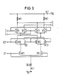
- FIG. 3 A second possible solution for the sum part is shown in FIG. 3.
- the connection is basically to be made as in the summation part according to FIG. 2, so that the same reference numerals are used in FIG. 2 and FIG. 3.
- the first MOS transistor MT1, the second and third transistors TR2 and TR3 are an n-channel MOS transistor and the first transistor TR1 and the second and third MOS transistor MT2, MT3 are a p-channel MOS transistor Transistor, while the first, second, third and fourth bipolar transistors BT1, BT2, BT3 and BT4 are in turn an npn bipolar transistor. Due to the design of the sum part according to FIG.
- first and second common input E1 ', E2' complementary input signals are no longer required and the inputs can be combined in pairs to form a first and second common input E1 ', E2'.
- the first common input E1 ' is given by a common connection of the first and second inputs E1, E2 and the second common input E2' by a common connection of the third and fourth inputs E3, E4.
- a disadvantage is a lower processing speed compared to a sum part in the first exemplary embodiment according to FIG. 2.
- FIG. 4 shows a first embodiment for the carry part of the adder cell.
- the carry part contains a first differential amplifier with a first MOS transistor MT1 and a first transistor TR1, a second differential amplifier with a second MOS transistor MT2 and a second transistor TR2, a third differential amplifier with a third MOS transistor MT3 and a third transistor TR3 and a fourth differential amplifier consisting of a first and second bipolar transistor BT1, BT2, a constant current source SQ and a first and second resistor W1, W2.
- a first connection of the first MOS transistor MT1 and a first one Terminal of the first transistor TR1 are connected together via the constant current source SQ to a first terminal Kl1 and a first terminal of the second MOS transistor MT2 and a first terminal of the second transistor TR2 are connected to a second terminal of the first MOS transistor MT1 and a first terminal of the third transistor TR3 and a first connection of the third MOS transistor MT3 are connected to a second connection of the first transistor TR1.
- a first connection of the first bipolar transistor BT1 and a first connection of the second bipolar transistor BT2 are also connected together to a second connection of the second MOS transistor MT2 and a second connection of the third transistor TR3, while a second connection of the second transistor TR2 and a second connection of the second bipolar transistor BT2 are connected together via a first resistor W1 to a second terminal KL2.
- a second connection of the first bipolar transistor BT1 and a second connection of the third MOS transistor MT3 are likewise connected to the second terminal KL2 via a second resistor W2.
- a first input E1 is connected to a control connection of the first transistor TR1, a second input E2 to a gate connection of the first MOS transistor MT1, while a control connection of the second transistor TR2 and a control connection of the third transistor TR3 jointly have a third input E3 and a gate terminal of the second MOS transistor MT2 and a gate terminal of the third MOS transistor MT3 together form a fourth input E4.
- a first carry input C for a non-inverted carry signal has a base connection of the second bipolar transistor BT2 and a second carry input C. for an inverted Carrysignal is connected to a base terminal of the first bipolar transistor BT1.
- a second connection of the first bipolar transistor BT1 and a second connection of the MOS transistor MT3 together form a first carry output C0 for a non-inverted carry output signal and a second connection of the second transistor TR2 and a second connection of the second bipolar transistor BT2 jointly provide a second carry output C0 for an inverted Carrysignal.
- the carry part of Figure 4 is the first terminal KL1 with the ground V SS and the second terminal KL2 with the supply voltage V DD .
- the first MOS transistor MT1 in the carry part is an n-channel MOS transistor
- the second and third MOS transistor MT2, MT3 a p-channel MOS transistor
- the first, second and third transistors TR1, TR2 and TR3 and the first and second bipolar transistors BT1, BT2 are npn bipolar transistors.
- the CMOS input signals to be summed are switched to the second and fourth inputs E2, E4, while corresponding reference signals, within the low and high level of the CMOS input signals, are applied to the first and third inputs.
- a comparison of the sum part according to FIG. 2 and the carry part according to FIG. 4 shows that in both circuits the differential amplifiers are connected according to a "series gating" principle. It can also be seen that time-critical paths, for example the Carrypath, are implemented in both circuits using bipolar or ECL technology, a level conversion between CMOS and ECL levels and a logical combination of the input signals is achieved in both circuits by the first three differential amplifiers executed.
- the first MOS transistor MT1 and the first transistor TR1 are an n-channel MOS transistor
- the first and second bipolar transistors BT1, BT2 are implemented by npn bipolar transistors.
- Such a design makes it necessary to operate the carry part according to FIG. 4 with input signals of opposite phase.
- the input signal at input E1 has an antiphase input signal to second input E2
- the input signal at third input E3 has an antiphase input signal to fourth input E4.
- the advantage of this variant is that it takes up less space, but is also part of such an implementation a longer runtime of the input signals in the circuit and thus a lower processing speed.
- FIG. 5 finally shows a second embodiment of a carry part for the adder cell, the basic structure of the circuit of the carry part according to Figure 4 corresponds.
- Bipolar transistors in the first three differential amplifiers are in turn replaced by MOS transistors here in such a way that complementary transistors form a current switch.
- the first MOS transistor MT1 and the second and third transistor TR2 and TR3 are an n-channel MOS transistor and the second and third MOS transistor MT2, MT3 are a p-channel MOS transistor, while the first and second Bipolar transistors BT1, BT2 are designed as npn bipolar transistors.
- This circuit has the advantage of requiring less space.
- MOS transistor type n- or p-channel in the circuits according to FIGS. 2 to 5 is made so that the MOS transistor size is minimal, which depends on the respective substrate bias of the MOS transistor. It is also possible to use only one type of MOS transistor in the sum or carry part.
- FIG. 6 shows a truth table for a carry and sum part of an adder cell, each of which is to be assigned complementary input signals.
- the first MOS transistor MT1 and the first transistor TR1 are n-channel MOS transistors
- the second and third MOS- Transistor MT2, MT3 and the second and third transistors TR2 and TR3 a p-channel MOS transistor and the first and second bipolar transistors according to FIG. 4 and the first, second, third and fourth bipolar transistors BT1, BT2, BT3 and BT4 respectively
- Figure 2 shows an npn bipolar transistor.
- the third line in the truth table according to FIG. 6, for example, indicates that a high level at the sum output S or at the sum output is precisely then S a low level occurs if the first and fourth inputs E1 and E4 as well as the carry input C. is connected to a high level and the second and third inputs E2, E3 and the carry input C are connected to a low level.
- a low level can be set at carry output C0 of the adder cell and at carry output C0 a high level can be tapped.
- the first and fourth bipolar transistors BT1, BT4 in the sum part according to FIG. 2 and the first bipolar transistor BT1 in the carry part according to FIG. 4 are turned on, while the second and third bipolar transistors BT2 and BT3 in the sum part according to FIG. 2 and the second bipolar transistor BT2 in FIG Carryteil is locked according to Figure 4.
- this causes a high level at the first sum output S and a high level at the second sum output S a low level and in the carry part of Figure 4 at the first carry output C0 a low level and a second carry output C0 a high level can be tapped.
Landscapes
- Engineering & Computer Science (AREA)
- Physics & Mathematics (AREA)
- General Physics & Mathematics (AREA)
- Theoretical Computer Science (AREA)
- Pure & Applied Mathematics (AREA)
- Mathematical Analysis (AREA)
- Computational Mathematics (AREA)
- Computing Systems (AREA)
- Mathematical Optimization (AREA)
- General Engineering & Computer Science (AREA)
- Amplifiers (AREA)
- Tone Control, Compression And Expansion, Limiting Amplitude (AREA)
- Logic Circuits (AREA)
Abstract
Description
- Die Erfindung betrifft eine Addierzelle mit einem Summen- und einem Carryteil.
- Bei einer großen Anzahl von digitalen Logikschaltungen, beispielsweise digitalen Filtern, Signalprozessoren und Mikroprozessoren werden Addierer benötigt. Das einfachste Prinzip für einen solchen Addierer ist das "Ripple-Carry"-Verfahren, bei dem ein entstehender Übertrag (Carry) seriell von einer Addiererzelle für das jeweils niederwertige Bit zu einer Addiererzelle für das jeweils höherwertige Bit übertragen wird. Die Durchlaufzeit das Übertragssignals bestimmt dabei im wesentlichen die Additionszeit. Auch aufwendigere Addiererprinzipien, wie z. B. das bekannte "Carry-Look-Ahead"-Verfahren, bauen auf Elementen des "Ripple-Carry"-Verfahrens auf.
- Addiererzellen zum Aufbau von Addieren für die oben angeführten Additionsverfahren in MOS-Schaltungstechnik sind beispielsweise aus H. Weiß, K. Horninger: "Integrierte MOS-Schaltungen", Springer-Verlag, Berlin-Heidelberg-New York (1982), auf den Seiten 188-194 bekannt.
- Neben der MOS-Schaltungstechnik hat sich in den letzten Jahren eine Bipolar-CMOS(BICMOS)-Schaltungstechnologie entwickelt, die besonders bei zeitkritischen und kompakten Schaltungen eingesetzt wird. Durch die Verwendung von "BICMOS"-Schaltungen ergeben sich Vorteile sowohl aus der MOS- als auch aus der Bipolar-Schaltungstechnologie. Hohe Packungsdichten und keine statische Verlustleistung, welche beispielsweise für Schaltungen aus der CMOS-Schaltungstechnik charakteristisch sind, eine geringe Offsetspannung sowie eine sehr hohe Verarbeitungsgeschwindigkeit, welche für Schaltungen in ECL- bzw. Bipolarschaltungstechnik kennzeichnend sind, sind Merkmale, die für eine Verwendung von Schaltungen in "BICMOS"-Schaltungstechno logie sprechen. Aus der technischen Literatur sind ebenfalls CMOS/Bipolarschaltungen für Addierer bekannt. In der Veröffentlichung IEEE Journal of Solid State Circuits, Vol. SC-21, No. 5, Okt. 1986, CMOS/Bipolar Circuits for 60 MHz Digital Processing, von Takashi Hotta et al ist in Fig. 7 eine 4-Bit-Recheneinheit angegeben, die aus Halbaddierer, einer "Carry-Generation"-Schaltung und einer "Carry-Propagation"-Schaltung besteht. In Fig. 8 und auf den Seiten 810 bzw. 811 ist die "Carry-Propagation"-Schaltung näher beschrieben, wobei in dieser Figur auch die Anwendung der "BICMOS"-Schaltungstechnologie erkennbar ist. Die "Carry-Propagation"-Schaltung enthält sowohl MOS-Transistoren als auch einen Bipolartransistor. Als Eingangssignale für diese Schaltung sind CMOS-Pegel zwischen 0 und 5 Volt vorgesehen, während an dem Ausgang dieser Schaltung ECL-Hübe im Millivoltbereich abgegriffen werden können.
- Bei der Schaltung in der zuletzt genannten Veröffentlichung, wird die Umsetzung der Eingangs-/Ausgangspegel und die Logikverarbeitung jeweils in getrennten Stufen vorgenommen. Hierbei dient in Fig. 8 ein Bipolarausgangstransistor zur Umwandlung in CMOS-Pegel, während die übrigen MOS-Transistoren der Schaltung für die Logikfunktion der Schaltung zuständig ist. Eine solche Schaltung nutzt die Geschwindigkeitsvorteile der "BICMOS"-Schaltungstechnologie nicht voll aus. Den bekannten Addiererzellen in der MOS-Schaltungstechnik haftet der Nachteil an, daß in dem Übertragspfad, der zeitkritsch für die gesamte Rechenzeit eines mit derartigen Addiererzellen aufgebauten Rechenwerks ist, entweder eine verhältnismäßig große Anzahl von Gattern eingefügt ist und/oder daß die in den Übertragspfad eingefügten Gatter Bestandteile von Kombinationsgattern sind. Im ersteren Fall wirkt sich die Anzahl von in Reihe geschalteten Gattern ungünstig auf die Durchlaufzeit von Übertragungssignalen aus. Im zweiten Fall wirkt sich unter Umständen zusätzlich die Tatsache ungünstig aus, daß die Aufladung der Kapazität des Übertragsausgangs aufgrund der relativen Hochohmigkeit der als Bestandteile von Kombinationsgattern ausgebildeten Gatter nicht mit der erforderlichen Flankensteilheit erfolgt.
- Der Erfindung liegt die Aufgabe zugrunde, Addiererzellen mit einem Summations- und einem Carryteil vorzustellen, bei der die Nachteile bekannter Addiererzellen bezüglich des Übertragspfades wirksam vermieden werden kann und die außerdem einen geringen Flächen- und Leistungsbedarf erfordern.
- Diese Aufgabe wird erfindungsgemäß durch die kennzeichnenden Merkmale im Patentanspruch 1 und Patentanspruch 5 gelöst.
- Eine weitere Ausgestaltung der Erfindung ist in den Unteransprüchen angegeben und wird in diesen näher erläutert.
- Die mit der Erfindung erzielten Vorteile bestehen insbesondere darin, daß die Addierzelle mit einem Summen- und einem Carryteil eine erheblich höhere Verarbeitungsgeschwindigkeit aufweist als Addierzellen in MOS-Schaltungstechnik. Die Vorteile der bipolaren bzw. ECL-Schaltungstechnik, wie geringe Offsetspannung und schnelle Verarbeitungsgeschwindigkeit sind weitere Vorteile dieser Addierzelle.
- Zwei Ausführungsbeispiele sind in den Figuren 2 und 3 bzw. Figur 4 und 5 wiedergegeben und werden im folgenden näher beschrieben. Es zeigen
- Figur 1 die Zusammenschaltung der Addierzellen mit je einem Summen- und je einem Carryteil zu einem gesamten Addierer,
- Figur 2 ein erstes Ausführungsbeispiel für den Summenteil der Addierzelle,
- Figur 3 ein zweites Ausführungsbeispiel für den Summenteil der Addierzelle,
- Figur 4 ein erstes Ausführungsbeispiel für den Carryteil der Addierzelle,
- Figur 5 ein zweites Ausführungsbeispiel für den Carryteil der Addierzelle,
- Figur 6 eine Wahrheitstabelle für die Addierzelle.
- Figur 1 zeigt die Verschaltung von n Addierzellen mit jeweils einem Summen- und einem Carryteil. Auf die erste Addierzelle, bestehend aus einem ersten Summen- ST1 und einem ersten Carryteil CT1, sind jeweils Eingangssignale auf die vier Eingänge E1,1 ... E4,1 und zwei Carryeingangssignale auf die zwei Carryeingänge C1,
C1 geschaltet. Die beiden Carryeingangssignale werden im ersten Carryteil CT1 auf einen festen "0"- bzw. "1"-Pegel gelegt. Carryausgangssignale aus dem ersten Carryteil CT1 bilden gleichzeitig die Carryeingangssignale an den zwei Carryeingängen C2,C2 für den zweiten Carryteil CT2 der zweiten Addierzelle. Diese Carryeingangssignale sind ebenfalls auf den zweiten Summenteil ST2 der zweiten Addierzelle geschaltet. Der zweite Summenteil ST2 als auch der zweite Carryteil CT2 sind ebenfalls wieder jeweils mit Eingangssignalen auf den vier Eingängen E1,2 ... E4,2 beschaltet. Die angegebene Verschaltung gilt für alle übrigen Addierzellen, so daß die n-te Addierzelle mit dem n-ten Summenteil STn und dem n-ten Carryteil CTn wiederum jeweils mit Carryeingangssignalen auf zwei Carryeingängen Cn,Cn und jeweils mit Eingangssignale auf vier Eingängen E1,n ...E4,n belegt ist. Die einzelnen Addierzellen weisen jeweils zwei Summenausgänge auf, die für den ersten Summenteil mit S1,S1 , für den zweiten Summenteil mit S2,S2 bzw. für den n-ten Summenteil Sn,Sn angegeben sind. Die Belegung der Eingangssignale für die einzelnen Addierzellen ist abhängig von dem gewählten Ausführungsbeispiel des Summenteils bzw. des Carryteils. Dies wird in den nachfolgenden Figuren 2 bis 6 nochmals näher erläutert. Die Carryeingangssignale an den Carryeingängen C1,C1 bzw. C2,C2 oder auch Cn,Cn sowie die Summenausgangssignale an den Summenausgängen S1,S1 bzw. S2,S2 oder auch Sn,Sn beinhalten jeweils komplementäre Signale. Die Belegung der einzelnen Carrysignale bzw. der Summenausgangssignale sind in Figur 6 in Tabellenform nochmals näher angegeben. - Figur 2 zeigt ein erstes Ausführungsbeispiel für einen Summenteil der Addierzelle. Der Summenteil enthält hierbei einen ersten Differenzverstärker mit einem ersten MOS-Transistor MT1 und einen ersten Transistor TR1, einen zweiten Differenzverstärker mit einem zweiten MOS-Transistor MT2 und einen zweiten Transistor TR2, einen dritten Differenzverstärker mit einem dritten MOS-Transistor MT3 und einem dritten Transistor TR3 sowie einen vierten Differenzverstärker, bestehend aus einem ersten und zweiten Bipolartransistor BT1, BT2, und einem fünften Differenzverstärker, bestehend aus einem dritten und vierten Bipolartransistor BT3, BT4 sowie eine Konstantstromquelle SQ und einen ersten und zweiten Widerstand W1 und W2. Nach Figur 2 ist ein erster Anschluß des ersten MOS-Transistors MT1 und ein erster Anschluß des ersten Transistors TR1 gemeinsam über die Konstantstromquelle SQ mit einer ersten Klemme KL1 verbunden und ein erster Anschluß des zweiten MOS-Transistors MT2 und ein erster Anschluß des zweiten Transistors TR2 ist mit einem zweiten Anschluß des ersten MOS-Transistors MT1 und ein erster Anschluß des dritten MOS-Transistors MT3 und ein erster Anschluß des dritten Transistors TR3 ist mit einem zweiten Anschluß des ersten Transistors TR1 verschaltet. Ein erster Anschluß des ersten Bipolartransistors BT1 und ein erster Anschluß des zweiten Bipolartransistors BT2 sind an einen zweiten Anschluß des zweiten MOS-Transistors MT2 und an einen zweiten Anschluß des dritten Transistors TR3 aufgeschaltet und ein erster Anschluß des dritten Bipolartransistors BT3 und ein erster Anschluß des vierten Bipolartransistors BT4 ist mit einem zweiten Anschluß des zweiten Transistors TR2 und mit einem zweiten Anschluß des dritten MOS-Transistors MT3 verschaltet. Ein zweiter Anschluß des ersten Bipolartransistors BT1 und ein zweiter Anschluß des dritten Bipolartransistors BT3 sind gemeinsam über einen ersten Widerstand W1 mit einer zweiten Klemme KL2 verschaltet und ein zweiter Anschluß des zweiten Bipolartransistors BT2 und ein zweiter Anschluß des vierten Bipolartransistors BT4 sind gemeinsam über einen zweiten Widerstand W2 ebenfalls mit der zweiten Klemme KL2 verbunden. Ein erster Eingang E1 ist mit einem Steueranschluß des ersten Transistors TR1, ein zweiter Eingang E2 mit einem Gateanschluß des ersten MOS-Transistors MT1 verschaltet und ein Steueranschluß des zweiten Transistors TR2 und ein Steueranschluß des dritten Transistors TR3 bilden gemeinsam einen dritten Eingang E3 und ein Gateanschluß des zweiten MOS-Transistors MT2 und ein Gateanschluß des dritten MOS-Transistors MT3 bilden wiederum einen vierten Eingang E4. Ein erster Carryeingang C für ein nicht invertiertes Carrysignal ist an einen Basisanschluß des zweiten Bipolartransistors BT2 und an einen Basisanschluß des dritten Bipolartransistors BT3 geschaltet, während ein zweiter Carryeingang
C für ein invertiertes Carrysignal mit einem Basisanschluß des ersten Bipolartransistors BT1 und einem Basisanschluß des vierten Bipolartransistors BT4 verbunden ist. Ein erster Summenausgang S für ein nicht invertiertes Summenausgangssignal ist nach Figur 2 mit dem zweiten Anschluß des vierten Bipolartransistors BT4 und mit dem zweiten Anschluß des zweiten Bipolartransistors BT2 verschaltet, während ein zweiter Anschluß des ersten Bipolartransistors BT1 und ein zweiter Anschluß des dritten Bipolartransistors BT3 gemeinsam einen zweiten SummenausgangS für ein invertiertes Summenausgangssignal bilden. Die erste Klemme KL1 ist in der Verschaltung des Summenteils mit der Masse VSS und die zweite Klemme KL2 mit der Versorgungsspannung VDD belegt. - Der Summenteil der Addierzelle nach Figur 2 sieht für den ersten MOS-Transistor MT1 einen n-Kanal-MOS-Transistors, für den zweiten und dritten MOS-Transistor MT2, MT3 einen p-Kanal-MOS-Transistor und für den ersten, zweiten und dritten Transistor TR1, TR2, TR3 sowie für den ersten, zweiten, dritten und vierten Bipolartransistor BT1, BT2, BT3 und BT4 einen npn-Bipolartransistor vor.
- In diesem Ausführungsbeispiel werden die zu summierenden CMOS-Eingangssignale auf den zweiten und vierten Eingang E2, E4 geschaltet, während auf den ersten und dritten Eingang entsprechende Referenzsignale, innerhalb des Low- und High-Pegels der CMOS-Eingangssignale, angelegt werden.
- Durch den Einsatz der "BICMOS"-Schaltungstechnik kann die Geschwindigkeit des Summenteils erheblich gegenüber einer Ausführung in reiner CMOS-Schaltungstechnologie gesteigert werden. Durch die Auslegung des vierten und fünften Differenzverstärkers in Bipolar- bzw. ECL-Technik weist der besonders zeitkritische Pfad für die Carrysignale eine besonders hohe Verarbeitungsgeschwindigkeit auf. Während auf der Eingangsseite E1, E2, E3 und E4 CMOS-Pegel zwischen 0 und 5 Volt erforderlich sind, werden für die Carrysignale am ersten und zweiten Carryeingang C,
C lediglich ECL-Hübe im Millivoltbereich erforderlich. Ebenfalls liefern die beiden Summenausgänge S,S ECL-Hübe, die zwischen 0 und einigen 100 Millivolt liegen. Dies ist der Fall, wenn der erste und zweite Widerstand W1, W2 in der Dimensionierung ungefähr 200 Ohm beträgt. Der Ausgangshub des Summensignals an den Summenausgängen S,S ist jedoch nicht nur von den Widerständen W1 und W2 abhängig, sondern ebenfalls von der Konstantstromquelle SQ, die sowohl in bipolarer als auch in MOS-Schaltungstechnik realisiert werden kann. Der Platzvorteil ergibt sich durch eine wesentlich geringere Anzahl von Bauelementen, der dadurch entsteht, daß sog. Pegelwandler, die CMOS-Schaltungspegel auf ECL-Pegel wandeln, entfallen. Der Leistungsvorteil des Summenteils nach Figur 2 ergibt sich durch eine geringere Anzahl von Querströmen in der Schaltung. - Eine andere Konfiguration der Transistoren ist für den Summenteil nach Figur 2 ebenfalls möglich. Hierbei ist der erste MOS-Transistor MT1 und der erste Transistor TR1 ein n-Kanal-MOS-Transistor, der zweite und dritte MOS-Transistor MT2, MT3 und der zweite und dritte Transistor TR2, TR3 ist als p-Kanal-MOS-Transistor und der erste, zweite, dritte und vierte Bipolartransistor BT1, BT2, BT3 und BT4 ist als npn-Bipolartransistor ausgeführt. Der Vorteil besteht in einem geringeren Flächenbedarf, während die größere Laufzeit durch die höhere Anzahl von MOS-Transistoren die Verarbeitungsgeschwindigkeit des Summenteils verringern. Die zuletzt angeführte Ausführungsform erfordert komplementäre Eingangssignale, so daß ein Eingangssignal am ersten Eingang E1 ein komplementäres Eingangssignal zu dem Eingangssignal am zweiten Eingang E2 und ein Eingangssignal am dritten Eingang E3 ein komplementäres Eingangssignal zu dem Eingangssignal am vierten Eingang E4 erfordert.
- Eine zweite Lösungsmöglichkeit für den Summenteil ist in Figur 3 dargestellt. Die Verschaltung ist grundsätzlich wie in dem Summenteil nach Figur 2 vorzunehmen, so daß gleiche Bezugszeichen in Figur 2 und Figur 3 Verwendung finden. Jedoch ist im Summenteil der erste MOS-Transistor MT1, der zweite und dritte Transistor TR2 und TR3 ein n-Kanal-MOS-Transistor und der erste Transistor TR1 und der zweite und dritte MOS-Transistor MT2, MT3 ein p-Kanal-MOS-Transistor, während der erste, zweite, dritte und vierte Bipolartransistor BT1, BT2, BT3 und BT4 wiederum ein npn-Bipolartransistor ist. Durch die Ausführung des Summenteils nach Figur 3 sind keine komplementären Eingangssignale mehr erforderlich und die Eingänge können paarweise zu einem ersten und zweiten gemeinsamen Eingang E1′, E2′ zusammengefaßt werden. Der erste gemeinsame Eingang E1′ ist durch eine gemeinsame Verschaltung des ersten und zweiten Eingangs E1, E2 und der zweite gemeinsame Eingang E2′ durch eine gemeinsame Verschaltung des dritten und vierten Eingangs E3, E4 gegeben. Für den Summenteil nach Figur 3 ergibt sich wiederum der Vorteil eines geringeren Flächenbedarfs, da keine komplementären Eingangssignale erforderlich sind. Von Nachteil ist eine niedrigere Verarbeitungsgeschwindigkeit gegenüber einem Summenteil im ersten Ausführungsbeispiel nach Fig. 2.
- Figur 4 zeigt ein erstes Ausführungsbeispiel für den Carryteil der Addierzelle. Der Carryteil enthält einen ersten Differenzverstärker mit einem ersten MOS-Transistor MT1 und einen ersten Transistor TR1, einen zweiten Differenzverstärker mit einem zweiten MOS-Transistor MT2 und einem zweiten Transistor TR2, einem dritten Differenzverstärker mit einem dritten MOS-Transistor MT3 und einem dritten Transistor TR3 und einen vierten Differenzverstärker, bestehend aus einem ersten und zweiten Bipolartransistor BT1, BT2, eine Konstantstromquelle SQ und einen ersten und zweiten Widerstand W1, W2. Ein erster Anschluß des ersten MOS-Transistors MT1 und ein erster Anschluß des ersten Transistors TR1 sind gemeinsam über die Konstantstromquelle SQ mit einer ersten Klemme Kl1 verbunden und ein erster Anschluß des zweiten MOS-Transistors MT2 und ein erster Anschluß des zweiten Transistors TR2 sind mit einem zweiten Anschluß des ersten MOS-Transistors MT1 und ein erster Anschluß des dritten Transistors TR3 und ein erster Anschluß des dritten MOS-Transistors MT3 sind mit einem zweiten Anschluß des ersten Transistors TR1 verschaltet. Ein erster Anschluß des ersten Bipolartransistors BT1 und ein erster Anschluß des zweiten Bipolartransistors BT2 sind weiterhin gemeinsam mit einem zweiten Anschluß des zweiten MOS-Transistors MT2 und einem zweiten Anschluß des dritten Transistors TR3 verbunden, während ein zweiter Anschluß des zweiten Transistors TR2 und ein zweiter Anschluß des zweiten Bipolartransistors BT2 gemeinsam über einen ersten Widerstand W1 mit einer zweiten Klemme KL2 verschaltet sind. Ein zweiter Anschluß des ersten Bipolartransistors BT1 und ein zweiter Anschluß des dritten MOS-Transistors MT3 sind gemeinsam über einen zweiten Widerstand W2 ebenfalls mit der zweiten Klemme KL2 verbunden. Ein erster Eingang E1 ist nach Figur 4 mit einem Steueranschluß des ersten Transistors TR1, ein zweiter Eingang E2 mit einem Gateanschluß des ersten MOS-Transistors MT1 verbunden, während ein Steueranschluß des zweiten Transistors TR2 und ein Steueranschluß des dritten Transistors TR3 gemeinsam einen dritten Eingang E3 und ein Gateanschluß des zweiten MOS-Transistors MT2 und ein Gateanschluß des dritten MOS-Transistors MT3 gemeinsam einen vierten Eingang E4 bilden. Ein erster Carryeingang C für ein nicht invertiertes Carrysignal ist mit einem Basisanschluß des zweiten Bipolartransistors BT2 und ein zweiter Carryeingang
C für ein invertiertes Carrysignal ist mit einem Basisanschluß des ersten Bipolartransistors BT1 verbunden. Ein zweiter Anschluß des ersten Bipolartransistors BT1 und ein zweiter Anschluß des MOS-Transistors MT3 bilden gemeinsam einen ersten Carryausgang C0 für ein nicht invertiertes Carryausgangssignal und ein zweiter Anschluß des zweiten Transistors TR2 und ein zweiter Anschluß des zweiten Bipolartransistors BT2 stellen gemeinsam einen zweiten CarryausgangC0 für ein invertiertes Carrysignal dar. Im Carryteil nach Figur 4 ist die erste Klemme KL1 mit der Masse VSS und die zweite Klemme KL2 mit der Versorgungsspannung VDD beschaltet. Der erste MOS-Transistor MT1 ist in dem Carryteil ein n-Kanal-MOS-Transistor, der zweite und dritte MOS-Transistor MT2, MT3 ein p-Kanal-MOS-Transistor, während der erste, zweite und dritte Transistor TR1, TR2 und TR3 sowie der erste und zweite Bipolartransistor BT1, BT2 npn-Bipolartransistoren sind. - In diesem Ausführungsbeispiel werden die zu summierenden CMOS-Eingangssignale auf den zweiten und vierten Eingang E2, E4 geschaltet, während auf den ersten und dritten Eingang entsprechende Referenzsignale, innerhalb des Low- und High-Pegels der CMOS-Eingangssignale, angelegt werden.
- Bei einem Vergleich des Summenteils nach Figur 2 und des Carryteils nach Figur 4 erkennt man, daß in beiden Schaltungen die Differenzverstärker nach einem "Series gating"-Prinzip verschaltet sind. Ebenfalls erkennt man, daß zeitkritische Pfade, beispielsweise der Carrypfad, in beiden Schaltungen in Bipolar- bzw. ECL-Technik ausgeführt ist, eine Pegelwandlung zwischen CMOS- und ECL-Pegel sowie eine logische Verknüpfung der Eingangssignale wird in beiden Schaltungen durch die ersten drei Differenzverstärker ausgeführt.
- Eine weitere Variante des Carryteils nach Figur 4 ergibt sich dadurch, daß der erste MOS-Transistor MT1 und der erste Transistor TR1 ein n-Kanal-MOS-Transistor, der zweite und dritte MOS-Transistor MT2 und MT3 sowie der zweite und dritte Transistor TR2 und TR3 und p-Kanal-MOS-Transistor ist und der erste und zweite Bipolartransistor BT1, BT2 durch npn-Bipolartransistoren ausgeführt sind. Durch eine solche Ausführung ist es erforderlich, den Carryteil nach Figur 4 mit gegenphasigen Eingangssignalen zu betrieben. In diesem Falle weist das Eingangssignal am Eingang E1 ein gegenphasiges Eingangssignal auf zum zweiten Eingang E2 und das Eingangssignal am dritten Eingang E3 ein gegenphasiges Eingangssignal zum vierten Eingang E4. Der Vortiel dieser Variante liegt in einem geringeren Flächenbedarf, jedoch ist bei einer solchen Realisierung mit einer größeren Laufzeit der Eingangssignale in der Schaltung und somit mit einer niedrigen Verarbeitungsgeschwindigkeit zu rechnen.
- Figur 5 schließlich zeigt ein zweites Ausführungsbeispiel eines Carryteils für die Addierzelle, wobei der grundsätzliche Aufbau der Schaltung des Carryteils nach Figur 4 entspricht. Aus diesem Grunde werden auch gleiche Bezugszeichen in der Fig. 4 und der Fig.5 verwendet. Bipolare Transistoren in den ersten drei Differenzverstärkern sind hier wiederum durch MOS-Transistoren ersetzt und zwar so, daß jeweils komplementäre Transistoren einen Stromschalter bilden. Der erste MOS-Transistor MT1 und der zweite und dritte Transistor TR2 und TR3 sind dabei ein n-Kanal-MOS-Transistor und der zweite und dritte MOS-Transistor MT2, MT3 ein p-Kanal-MOS-Transistor, während der erste und zweite Bipolartransistor BT1, BT2 als npn-Bipolartransistoren ausgeführt sind. Diese Schaltung hat den Vorteil eines geringeren Flächenbedarfs. Es werden hierfür keine komplementären Eingangssignale erforderlich, so daß der erste und zweite Eingang E1, E2 zu einem ersten gemeinsamen Eingang E1′ und der dritte und vierte Eingang E3, E4 zu einem gemeinsamen zweiten Eingang E2′ zusammengefaßt werden können. Nachteilig an diesem zweiten Ausführungsbeispiel ist ebenfalls die etwas niedrigere Verarbeitungsgeschwindigkeit gegenüber der Schaltung nach Figur 4.
- Die Wahl des MOS-Transistortyps n- bzw. p-Kanal bei den Schaltungen nach Figur 2 bis 5 erfolgt so, daß die MOS-Transistorgröße minimal ist, was von der jeweiligen Substratvorspannung des MOS-Transistors abhängt. Es ist ebenfalls möglich, jeweils nur einen MOS-Transistortyp in dem Summen- bzw. Carryteil zu verwenden.
- Figur 6 zeigt eine Wahrheitstabelle für ein Carry- und Summenteil einer Addierzelle, die jeweils mit komplementären Eingangssignalen zu belegen sind. In diesem Falle sind in beiden Schaltungen der erste MOS-Transistor MT1 und der erste Transistor TR1 n-Kanal-MOS-Transistoren, der zweite und dritte MOS- Transistor MT2, MT3 und der zweite und dritte Transistor TR2 und TR3 ein p-Kanal-MOS-Transistor und der erste und zweite Bipolartransistor nach Fig. 4 bzw. der erste, zweite, dritte und vierte Bipolartransistor BT1, BT2, BT3 und BT4 nach Figur 2 ein npn-Bipolartransistor. In der ersten Spalte E1 =
E2 sind die komplementären Eingangssignale zum zweiten Eingang E2 aufgezeigt, während im dritten Eingang E3 =E4 die komplementären Eingangssignale des vierten Eingang E4 aufgeführt sind. Ein erster und zweiter Carryeingang, C,C für ein nicht invertiertes bzw. invertiertes Carrysignal sind ebenfalls in der Wahrheitstabelle nach Figur 6 angegeben. Für den Summenteil der Addierzelle sind die Ausgangssignale am Summenausgang S undS in der Wahrheitstabelle aufgeführt, während für den Carryteil die Ausgangssignale am Carryausgang C0 bzw.C0 wiedergegeben sind. - Stellvertretend für die übrigen Zeilen gibt beispielsweise die dritte Zeile in der Wahrheitstabelle nach Figur 6 an, daß am Summenausgang S genau dann ein High-Pegel bzw. am Summenausgang
S ein Low-Pegel auftritt, falls der erste und vierte Eingang E1 und E4 sowie der CarryeingangC mit einem High-Pegel und der zweite und dritte Eingang E2, E3 sowie der Carryeingang C mit einem Low-Pegel beschaltet ist. In diesem Falle können am Carryausgang C0 der Addierzelle ein Low-Pegel und am CarryausgangC0 ein High-Pegel abgegriffen werden. Für den Summen- bzw. Carryteil nach Figur 2 bzw. 4 bedeutet dies, daß der erste Transistor TR1 leitet und der erste MOS-Transistor MT1 sperrt, daß der zweite und dritte MOS-Transistor MT2, MT3 sperrt und der zweite und dritte Transistor TR2, TR3 leitet. Der erste und vierte Bipolartransistor BT1, BT4 im Summenteil nach Fig. 2 bzw. der erste Bipolartransistor BT1 im Carryteil nach Figur 4 ist durchgeschaltet, während der zweite und dritte Bipolartransistor BT2 und BT3 im Summenteil nach Fig. 2 bzw. der zweite Bipolartransistor BT2 im Carryteil nach Figur 4 gesperrt ist. Dies bewirkt im Summenteil nach Figur 2, daß am ersten Summenausgang S ein High-Pegel und am zweiten SummenausgangS ein Low-Pegel und im Carryteil nach Figur 4 am ersten Carryausgang C0 ein Low-Pegel und ein zweiten CarryausgangC0 ein High-Pegel abgegriffen werden kann.
Claims (9)
Applications Claiming Priority (2)
| Application Number | Priority Date | Filing Date | Title |
|---|---|---|---|
| DE3803542 | 1988-02-05 | ||
| DE3803542 | 1988-02-05 |
Publications (3)
| Publication Number | Publication Date |
|---|---|
| EP0326897A2 true EP0326897A2 (de) | 1989-08-09 |
| EP0326897A3 EP0326897A3 (de) | 1991-05-22 |
| EP0326897B1 EP0326897B1 (de) | 1995-04-05 |
Family
ID=6346746
Family Applications (1)
| Application Number | Title | Priority Date | Filing Date |
|---|---|---|---|
| EP89101130A Expired - Lifetime EP0326897B1 (de) | 1988-02-05 | 1989-01-23 | Addierzelle mit einem Summen- und einem Carryteil |
Country Status (4)
| Country | Link |
|---|---|
| US (1) | US4918640A (de) |
| EP (1) | EP0326897B1 (de) |
| JP (1) | JPH01226028A (de) |
| DE (1) | DE58909149D1 (de) |
Cited By (1)
| Publication number | Priority date | Publication date | Assignee | Title |
|---|---|---|---|---|
| FR2724073A1 (fr) * | 1994-08-31 | 1996-03-01 | Sgs Thomson Microelectronics | Circuit logique a etages differentiels |
Families Citing this family (8)
| Publication number | Priority date | Publication date | Assignee | Title |
|---|---|---|---|---|
| US5113095A (en) * | 1990-08-29 | 1992-05-12 | Motorola, Inc. | BiCMOS logic circuit with a CML output |
| US5163020A (en) * | 1991-04-15 | 1992-11-10 | Texas Instruments Incorporated | High speed BiCMOS conditional sum adder |
| US5175703A (en) * | 1991-04-29 | 1992-12-29 | Motorola, Inc. | High speed full adder and method |
| US5268858A (en) * | 1991-08-30 | 1993-12-07 | Cyrix Corporation | Method and apparatus for negating an operand |
| US5539332A (en) * | 1994-10-31 | 1996-07-23 | International Business Machines Corporation | Adder circuits and magnitude comparator |
| US5818747A (en) * | 1995-01-27 | 1998-10-06 | Sun Microsystems, Inc. | Small, fast CMOS 4-2 carry-save adder cell |
| US6037891A (en) * | 1998-02-23 | 2000-03-14 | Motorola, Inc. | Low power serial analog-to-digital converter |
| US6373377B1 (en) | 2000-10-05 | 2002-04-16 | Conexant Systems, Inc. | Power supply with digital data coupling for power-line networking |
Family Cites Families (4)
| Publication number | Priority date | Publication date | Assignee | Title |
|---|---|---|---|---|
| US3519810A (en) * | 1967-02-14 | 1970-07-07 | Motorola Inc | Logic element (full adder) using transistor tree-like configuration |
| JPS60205631A (ja) * | 1984-03-29 | 1985-10-17 | Toshiba Corp | 全加算回路 |
| JPS60247733A (ja) * | 1984-05-24 | 1985-12-07 | Toshiba Corp | 論理演算回路 |
| JPS60247734A (ja) * | 1984-05-24 | 1985-12-07 | Toshiba Corp | 論理演算回路 |
-
1989
- 1989-01-12 US US07/296,070 patent/US4918640A/en not_active Expired - Fee Related
- 1989-01-23 EP EP89101130A patent/EP0326897B1/de not_active Expired - Lifetime
- 1989-01-23 DE DE58909149T patent/DE58909149D1/de not_active Expired - Fee Related
- 1989-01-31 JP JP1023652A patent/JPH01226028A/ja active Pending
Cited By (2)
| Publication number | Priority date | Publication date | Assignee | Title |
|---|---|---|---|---|
| FR2724073A1 (fr) * | 1994-08-31 | 1996-03-01 | Sgs Thomson Microelectronics | Circuit logique a etages differentiels |
| EP0700162A1 (de) * | 1994-08-31 | 1996-03-06 | STMicroelectronics S.A. | Logische Schaltung mit Differenzstufen |
Also Published As
| Publication number | Publication date |
|---|---|
| US4918640A (en) | 1990-04-17 |
| EP0326897A3 (de) | 1991-05-22 |
| JPH01226028A (ja) | 1989-09-08 |
| DE58909149D1 (de) | 1995-05-11 |
| EP0326897B1 (de) | 1995-04-05 |
Similar Documents
| Publication | Publication Date | Title |
|---|---|---|
| DE3853805T2 (de) | Digitaler Multiplizierer und Multiplizierer-Akkumulator, welcher Zwischenergebnisse vorlädt und akkumuliert. | |
| DE69418012T2 (de) | Frequenzmultiplizierer mit einer Baumstruktur von CMOS logischen Gattern des Typs "Exclusiv-ODER" | |
| DE69030257T2 (de) | Logisch programmierbare ausdehnungsvorrichtung | |
| DE3877062T2 (de) | Anordnung fuer cmos-integrierten schaltungsaufbau eines logischen baumes mit eingangsbelastbarkeit. | |
| DE3607045A1 (de) | Digitale addier- und subtrahierschaltung | |
| EP0122946B1 (de) | CMOS-Volladdierstufe | |
| DE2649725C2 (de) | ||
| DE3840969A1 (de) | Integrierte halbleiter-schaltungsvorrichtung | |
| DE68926518T2 (de) | Flipflop-Schaltung | |
| EP0326897B1 (de) | Addierzelle mit einem Summen- und einem Carryteil | |
| DE2522797C3 (de) | Flip-Flop-Schaltung | |
| DE3940897C2 (de) | Schaltungsanordnung und Verfahren zur Berechnung digitaler Summen in einem Halbleiteraddierer mit Parallelübertrag | |
| DE68916093T2 (de) | Integrierte Schaltung. | |
| EP0252999B1 (de) | Getaktete CMOS-Schaltung mit mindestens einem CMOS-Schalter | |
| DE2743450A1 (de) | Sperrbare zaehlerstufe | |
| EP0048352B1 (de) | Binärer MOS-Switched-Carry-Paralleladdierer | |
| EP0352549B1 (de) | Carry-select-Addierer | |
| DE3828290C2 (de) | ||
| DE3610875A1 (de) | Subtrahierer in komplementaerer metalloxid-halbleitertechnologie | |
| DE3788132T2 (de) | Logische Schaltkreisfamilie von Multibasis-bi-CMOS. | |
| EP0224656B1 (de) | Mehrstelliger Carry-Ripple-Addierer in CMOS-Technik mit zwei Typen von Addiererzellen | |
| DE3751085T2 (de) | Volladdiererschaltung. | |
| DE69513278T2 (de) | Kombinierte pla- und pal-schaltung | |
| DE3784838T2 (de) | Vorwaerts-/rueckwaerts-n-bit-zaehlregister. | |
| DE1814496A1 (de) | Schaltanordnung mit Haupt- und Tochterschalter |
Legal Events
| Date | Code | Title | Description |
|---|---|---|---|
| PUAI | Public reference made under article 153(3) epc to a published international application that has entered the european phase |
Free format text: ORIGINAL CODE: 0009012 |
|
| AK | Designated contracting states |
Kind code of ref document: A2 Designated state(s): DE FR GB |
|
| 17P | Request for examination filed |
Effective date: 19901205 |
|
| PUAL | Search report despatched |
Free format text: ORIGINAL CODE: 0009013 |
|
| AK | Designated contracting states |
Kind code of ref document: A3 Designated state(s): DE FR GB |
|
| 17Q | First examination report despatched |
Effective date: 19940603 |
|
| GRAA | (expected) grant |
Free format text: ORIGINAL CODE: 0009210 |
|
| AK | Designated contracting states |
Kind code of ref document: B1 Designated state(s): DE FR GB |
|
| REF | Corresponds to: |
Ref document number: 58909149 Country of ref document: DE Date of ref document: 19950511 |
|
| GBT | Gb: translation of ep patent filed (gb section 77(6)(a)/1977) |
Effective date: 19950616 |
|
| ET | Fr: translation filed | ||
| PLBE | No opposition filed within time limit |
Free format text: ORIGINAL CODE: 0009261 |
|
| STAA | Information on the status of an ep patent application or granted ep patent |
Free format text: STATUS: NO OPPOSITION FILED WITHIN TIME LIMIT |
|
| 26N | No opposition filed | ||
| PGFP | Annual fee paid to national office [announced via postgrant information from national office to epo] |
Ref country code: GB Payment date: 19961219 Year of fee payment: 9 |
|
| PGFP | Annual fee paid to national office [announced via postgrant information from national office to epo] |
Ref country code: FR Payment date: 19970123 Year of fee payment: 9 |
|
| PGFP | Annual fee paid to national office [announced via postgrant information from national office to epo] |
Ref country code: DE Payment date: 19970317 Year of fee payment: 9 |
|
| PG25 | Lapsed in a contracting state [announced via postgrant information from national office to epo] |
Ref country code: GB Free format text: LAPSE BECAUSE OF NON-PAYMENT OF DUE FEES Effective date: 19980123 |
|
| PG25 | Lapsed in a contracting state [announced via postgrant information from national office to epo] |
Ref country code: FR Free format text: THE PATENT HAS BEEN ANNULLED BY A DECISION OF A NATIONAL AUTHORITY Effective date: 19980131 |
|
| GBPC | Gb: european patent ceased through non-payment of renewal fee |
Effective date: 19980123 |
|
| PG25 | Lapsed in a contracting state [announced via postgrant information from national office to epo] |
Ref country code: DE Free format text: LAPSE BECAUSE OF NON-PAYMENT OF DUE FEES Effective date: 19981001 |
|
| REG | Reference to a national code |
Ref country code: FR Ref legal event code: ST |