EP0327111A2 - Laser à diamant et méthode de fabrication et de mise en oeuvre - Google Patents
Laser à diamant et méthode de fabrication et de mise en oeuvre Download PDFInfo
- Publication number
- EP0327111A2 EP0327111A2 EP89101933A EP89101933A EP0327111A2 EP 0327111 A2 EP0327111 A2 EP 0327111A2 EP 89101933 A EP89101933 A EP 89101933A EP 89101933 A EP89101933 A EP 89101933A EP 0327111 A2 EP0327111 A2 EP 0327111A2
- Authority
- EP
- European Patent Office
- Prior art keywords
- diamond
- laser
- pumping light
- centers
- range
- Prior art date
- Legal status (The legal status is an assumption and is not a legal conclusion. Google has not performed a legal analysis and makes no representation as to the accuracy of the status listed.)
- Granted
Links
Images


Classifications
-
- H—ELECTRICITY
- H01—ELECTRIC ELEMENTS
- H01S—DEVICES USING THE PROCESS OF LIGHT AMPLIFICATION BY STIMULATED EMISSION OF RADIATION [LASER] TO AMPLIFY OR GENERATE LIGHT; DEVICES USING STIMULATED EMISSION OF ELECTROMAGNETIC RADIATION IN WAVE RANGES OTHER THAN OPTICAL
- H01S3/00—Lasers, i.e. devices using stimulated emission of electromagnetic radiation in the infrared, visible or ultraviolet wave range
- H01S3/14—Lasers, i.e. devices using stimulated emission of electromagnetic radiation in the infrared, visible or ultraviolet wave range characterised by the material used as the active medium
- H01S3/16—Solid materials
-
- C—CHEMISTRY; METALLURGY
- C30—CRYSTAL GROWTH
- C30B—SINGLE-CRYSTAL GROWTH; UNIDIRECTIONAL SOLIDIFICATION OF EUTECTIC MATERIAL OR UNIDIRECTIONAL DEMIXING OF EUTECTOID MATERIAL; REFINING BY ZONE-MELTING OF MATERIAL; PRODUCTION OF A HOMOGENEOUS POLYCRYSTALLINE MATERIAL WITH DEFINED STRUCTURE; SINGLE CRYSTALS OR HOMOGENEOUS POLYCRYSTALLINE MATERIAL WITH DEFINED STRUCTURE; AFTER-TREATMENT OF SINGLE CRYSTALS OR A HOMOGENEOUS POLYCRYSTALLINE MATERIAL WITH DEFINED STRUCTURE; APPARATUS THEREFOR
- C30B29/00—Single crystals or homogeneous polycrystalline material with defined structure characterised by the material or by their shape
- C30B29/02—Elements
- C30B29/04—Diamond
-
- C—CHEMISTRY; METALLURGY
- C30—CRYSTAL GROWTH
- C30B—SINGLE-CRYSTAL GROWTH; UNIDIRECTIONAL SOLIDIFICATION OF EUTECTIC MATERIAL OR UNIDIRECTIONAL DEMIXING OF EUTECTOID MATERIAL; REFINING BY ZONE-MELTING OF MATERIAL; PRODUCTION OF A HOMOGENEOUS POLYCRYSTALLINE MATERIAL WITH DEFINED STRUCTURE; SINGLE CRYSTALS OR HOMOGENEOUS POLYCRYSTALLINE MATERIAL WITH DEFINED STRUCTURE; AFTER-TREATMENT OF SINGLE CRYSTALS OR A HOMOGENEOUS POLYCRYSTALLINE MATERIAL WITH DEFINED STRUCTURE; APPARATUS THEREFOR
- C30B33/00—After-treatment of single crystals or homogeneous polycrystalline material with defined structure
Definitions
- the present invention relates to a diamond laser and a method of producing the same and a method of acting the same and particularly it relates to a diamond laser capable of varying wavelength in the near infrared region and a method of producing the same and a method of acting the same.
- H2 color centers are not formed in type Ib diamond and that they coexist with H3 centers, and have low absorption in natural type Ia diamond.
- a conventional method of forming H2 color centers comprises the step of heat-treating, at 627°C, natural Ia type diamond containing not less than 1019 nitrogen atoms/cm3. In this case, heating at 227 - 327°C in dark places increases H2 centers but decreases H3 centers. Further, with the conventional method, it is impossible to form H2 centers from type IIa and type Ib diamonds.
- lasers which are capable of varying wavelengths in the near infrared region include the F center laser using alkali halide single crystals and the dye laser.
- the lasing wavelength of said F center laser is in the ranges of 1400 - 1600 nm and 2200 - 3300 nm in the range of 1000 - 1400 nm laser action is impossible.
- the wavelength range in which the dye laser oscillates continuously is 330 - 1050 nm and 1100 - 1200 nm.
- the range in which the laser output power is high is 400 - 800 nm, and the output power in the near infrared region is very low.
- the conventional near infrared lasers have the following drawbacks:
- An object of the present invention is to provide a diamond laser which uses diamond as a laser medium heretofore not used and which produces high output power and is capable of varying wavelengths in the near infrared region. Further, the invention also makes it possible to provide a small-sized high output power laser capable of varying wavelength.
- the maximum optical density of H2 centers in the direction of the pumping light in a synthetic diamond is the range of 0.01 - 4 and laser action is effected in the range of 1000 - 1400 nm by external pumping light at 650 - 950 nm.
- a first method of producing said diamond laser according to the invention comprises the steps of subjecting synthetic type Ib diamond whose nitrogen concentration is 1 x 10¹⁷ - 8.5 x 10¹⁹ atoms/cm3, to electron irradiation to a dose of not less than 5 x 10¹⁷ electrons/cm2, and heat-treating it in the temperature range of 1400 - 1850°C in a vacuum at not more than 1 Torr or in an inert gas atmosphere.
- a second method of producing said diamond laser according to the invention comprises the steps of subjecting synthetic diamond whose nitrogen concentration is 1 x 10¹⁷ - 8.5 x 10¹⁹ atoms/cm3, to electron irradiation to a dose of 5 x 10¹⁷ electrons/cm2, and heat treating it under ultrahigh pressure and high temperature conditions at not less than 3.0 GPa and not less than 1500°C.
- a method of acting said diamond laser comprises the step of using laser as said external pumping light.
- a single or plural semiconductor lasers may be used for said external pumping light.
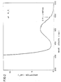
- Fig. 1 shows a pumping light intensity distribution in a crystal with a thickness T when pumping light with I0 falls on the crystal.
- a solid line 1 indicates a typical distribution in which the optical density is within the range of the invention, and a broken line 2 indicates a comparative example in which the optical density is greater than the limit value.
- I and Ia indicate their respective intensities on the transmission side.
- Ith indicates the threshold value required for laser oscillation.
- the optical intensity in order to obtain a pumping light distribution in which the intensity is higher than Ith, the lower the optical intensity, the better. If the optical intensity is too high, the exciting light intensity becomes lower than Ith, which is necessary for laser action, in some crystals. Therefore, in such locations, laser action does not occur. To ensure that laser action occurs throughout the crystal, it is important that the pumping light intensity be not less than Ith throughout the crystal. To this end, the optical density must be not more than 4. On the other hand, setting the optical density at too low a value means that the color center concentration decreases. If the color center concentration is too low, stimulated emission does not occur, nor does laser action. That is, if the optical density of H2 centers is less than 0.01, laser action does not occur. In addition, as can be seen from the foregoing description, said optical density value becomes important when it is in the same direction as the incident light (pumping light).
- H2 center will be formed with its optical density not more than 0.01. In the case of not less than 8.5 x 10¹⁹ atoms/cm3, the optical density will be not less than 4.
- diamond crystal small single crystals by the film growth method can be available, but it is preferable to use large-sized single crystals with high purity by the temperature gradient method.
- the present invention is characterized by a large amount of electron beam irradiation.
- color centers can be formed by using a relatively small amount of electron irradiation, but if the nitrogen is small, a large amount of electron irradiation is needed.
- the lower limit is 5 x 10¹⁷ electrons/cm2.
- it is 1 x 10¹⁸ - 1 x 10²³ electrons/cm2.
- the defects caused by electron beams can no longer be eliminated by the annealing described above in (3) and (4).
- the electron irradiation energy be in the range of 0.5 - 5 MeV.
- H2 centers are formed by heat treatment. Temperature condition is important; in a vacuum, not less than 1400°C is needed. However, if the temperature is not less than 1850°C, phase transformation takes place, so diamond changing into graphite. Unless heat treatment is effected at pressures not more than 1 Torr, the diamond surface is graphitized. In this case, inert gas, such as Ar or H2, may be used instead of vacuum.
- inert gas such as Ar or H2
- H2 centers are formed in the early stage of such annealing, and thereafter H2 centers are decreased. Therefore, by suitably selecting temperature condition and time for this annealing, the concentration of H2 centers can be controlled.
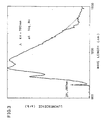
- H2 centers formed by the above method (1), (2), (4) are shown in Figs. 2 and 3.
- emission spectrum measurement a semiconductor laser with a wavelength of 780 nm was used as pumping light. It has been found that these centers have zerophonon line (ZPL) at a wavelength of 987 nm.
- ZPL zerophonon line
- the absorption of H2 centers lies in the range of 600 - 992 nm.
- the absorption peak lies at 800 nm, and it is in the range of 800 ⁇ 150 nm that pumping light works efficiently.
- Lamp light may be condensed to form an pumping light source, but the use of laser light is preferable since it provides higher conversion efficiency.
- a semiconductor laser for example, a laser with wavelength at 780 nm
- a wavelength tuning element such as grating, prism or etalon will be inserted in a resonator or in an optical path.
- H2 centers which has heretofore been impossible to form type Ib diamond can be formed with satisfactory reproducibility.
- a laser according to the invention enables laser action to be effected in the wavelength range of 1000 - 1400 nm.
- said laser effective if utilized for spectroanalysis, distance measurement, fine machining or other purposes.
- This example is an embodiment of the production method described in claim 2.
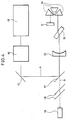
- the nitrogen concentration of diamonds was estimated from an absorption coefficient of 1130 cm ⁇ 1 by infrared spectral analysis. Further, optical density was measured by an instrument for spectroanalysis in visible region. Laser action was effected by using a laser system shown in Fig. 4.
- the numeral 11 denotes a laser crystal
- 12 denotes a total reflection mirror
- 13 denotes a translucent mirror
- 14 denotes a prism
- 15 denotes an argon ion laser
- 16 denotes a dye laser
- 17 denotes mirror for changing the optical path
- 18 denotes a filter
- 19 denotes a measuring instrument.
- the solid line A denotes pumping light and broken line B denotes laser light.
- This example is an embodiment of the production method described in claim 3.
- the No. 5 sample prepared in Example 1 was arranged with a Brewster angle as shown at the numeral 11 in Fig. 4.
- the total reflection mirror 12, tranlucent mirror 13 and prism 14 were arranged as shown in Fig. 4 to constitute a resonator.
- As an pumping light source use was made of an argon ion laser 15 and a dye laser 16.
- the argon ion laser 15 was used for pumping the dye laser 16. Since the dye laser 16 was capable of varying the wavelength, the laser light from the dye laser 16 was used as pumping light for samples.
- the laser light is amplified in the resonator constituted of the translucent mirror 13, total reflection mirror 12 and prism 14, and laser light was emitted. Stray light due to pumping light was cut by a filter 18, and the output and wavelength were measured by a power meter or wavelength measuring instrument 19.
- This example is an embodiment of claim 5.
- a laser apparatus shown in Fig. 5 was used.
- the numeral 21 denotes a grating
- 24 denotes a semiconductor laser array
- 25 denotes a condenser
- 26 denotes exciting light
- 27 denotes laser light
- 28 denotes a measuring instrument.
- eight semiconductor lasers whose wavelength is 780 nm were used to form the semiconductor array 24.
- an synthetic type Ib diamond was cut into a rod form having a diameter of 2 mm and a length of 10 mm, one longitudinal end surface being cut at the Brester angle.
- the nitrogen concentration of the sample was 3.5 x 10¹⁸ atoms/cm3.
- the sample was subjected to electron irradiation to a dose of 1 x 10¹⁹ electrons/cm2 with 3 MeV. Thereafter, ultrahigh pressure high temperature annealing at 3.0 GPa and 1800°C was carried out.
- the surface of the sample was made optical polish and then the vertical end surface was coated with a translucent film 22. Thereby, the crystal 21 shown in Fig. 5 was obtained.
- the crystal 21 was placed in the condenser 25 and the pumping light 26 was incident on the crystal 21 through a hole in the condenser 25.
- Wavelength selection was effected by adjusting the grating 23, whereby laser action occurred in the range 1000 - 1400 nm.
- the output power and laser wavelength were measured by a power meter or wavelength measurement 28.
Landscapes
- Chemical & Material Sciences (AREA)
- Engineering & Computer Science (AREA)
- Crystallography & Structural Chemistry (AREA)
- Materials Engineering (AREA)
- Metallurgy (AREA)
- Organic Chemistry (AREA)
- Physics & Mathematics (AREA)
- Electromagnetism (AREA)
- Plasma & Fusion (AREA)
- Optics & Photonics (AREA)
- Crystals, And After-Treatments Of Crystals (AREA)
- Lasers (AREA)
Applications Claiming Priority (2)
| Application Number | Priority Date | Filing Date | Title |
|---|---|---|---|
| JP26372/88 | 1988-02-05 | ||
| JP63026372A JPH01201976A (ja) | 1988-02-05 | 1988-02-05 | ダイヤモンド固体レーザ素子、その製造方法およびその発振方法 |
Publications (3)
| Publication Number | Publication Date |
|---|---|
| EP0327111A2 true EP0327111A2 (fr) | 1989-08-09 |
| EP0327111A3 EP0327111A3 (en) | 1990-03-14 |
| EP0327111B1 EP0327111B1 (fr) | 1991-06-12 |
Family
ID=12191681
Family Applications (1)
| Application Number | Title | Priority Date | Filing Date |
|---|---|---|---|
| EP89101933A Expired - Lifetime EP0327111B1 (fr) | 1988-02-05 | 1989-02-03 | Laser à diamant et méthode de fabrication et de mise en oeuvre |
Country Status (7)
| Country | Link |
|---|---|
| US (1) | US4949347A (fr) |
| EP (1) | EP0327111B1 (fr) |
| JP (1) | JPH01201976A (fr) |
| CA (1) | CA1294695C (fr) |
| DE (1) | DE68900111D1 (fr) |
| IE (1) | IE64619B1 (fr) |
| ZA (1) | ZA89897B (fr) |
Cited By (3)
| Publication number | Priority date | Publication date | Assignee | Title |
|---|---|---|---|---|
| CN111247276A (zh) * | 2017-10-20 | 2020-06-05 | 住友电气工业株式会社 | 合成单晶金刚石 |
| EP3699329A4 (fr) * | 2017-10-20 | 2021-06-30 | Sumitomo Electric Industries, Ltd. | Diamant monocristallin synthétique, outil, et procédé de production de diamant monocristallin synthétique |
| EP4067540A4 (fr) * | 2019-11-26 | 2022-12-28 | Sumitomo Electric Industries, Ltd. | Diamant monocristallin synthétique, outil équipé de celui-ci, et procédé de production de diamant monocristallin synthétique |
Families Citing this family (12)
| Publication number | Priority date | Publication date | Assignee | Title |
|---|---|---|---|---|
| US5488626A (en) * | 1991-01-14 | 1996-01-30 | Light Age, Inc. | Method of and apparatus for pumping of transition metal ion containing solid state lasers using diode laser sources |
| US5173761A (en) * | 1991-01-28 | 1992-12-22 | Kobe Steel Usa Inc., Electronic Materials Center | Semiconducting polycrystalline diamond electronic devices employing an insulating diamond layer |
| US5620754A (en) * | 1994-01-21 | 1997-04-15 | Qqc, Inc. | Method of treating and coating substrates |
| US5731046A (en) * | 1994-01-18 | 1998-03-24 | Qqc, Inc. | Fabrication of diamond and diamond-like carbon coatings |
| US5554415A (en) * | 1994-01-18 | 1996-09-10 | Qqc, Inc. | Substrate coating techniques, including fabricating materials on a surface of a substrate |
| US5524016A (en) * | 1994-06-09 | 1996-06-04 | Gte Laboratories Incorporated | Optical emitter for amplification and process for making same |
| US7224532B2 (en) * | 2002-12-06 | 2007-05-29 | Chevron U.S.A. Inc. | Optical uses diamondoid-containing materials |
| US20050019955A1 (en) * | 2003-07-23 | 2005-01-27 | Dahl Jeremy E. | Luminescent heterodiamondoids as biological labels |
| US11641088B2 (en) * | 2020-01-15 | 2023-05-02 | Emad Eskandar | Phased-array MASER detector for synthetic aperture interferometric imaging |
| JP7433957B2 (ja) * | 2020-02-12 | 2024-02-20 | 古河電気工業株式会社 | レーザ装置 |
| CN114136018B (zh) * | 2021-11-23 | 2023-09-01 | 北京量子信息科学研究院 | 激光制冷系统及激光制冷方法 |
| CN114061175B (zh) * | 2021-11-23 | 2023-08-01 | 北京量子信息科学研究院 | 激光制冷器及激光制冷方法 |
Family Cites Families (5)
| Publication number | Priority date | Publication date | Assignee | Title |
|---|---|---|---|---|
| US3970960A (en) * | 1974-01-31 | 1976-07-20 | Bell Telephone Laboratories, Incorporated | Broadly tunable continuous-wave laser using color centers |
| US4174380A (en) * | 1976-07-21 | 1979-11-13 | General Electric Company | Annealing synthetic diamond type Ib |
| US4124690A (en) * | 1976-07-21 | 1978-11-07 | General Electric Company | Annealing type Ib or mixed type Ib-Ia natural diamond crystal |
| US4638484A (en) * | 1984-11-20 | 1987-01-20 | Hughes Aircraft Company | Solid state laser employing diamond having color centers as a laser active material |
| EP0275063A3 (fr) * | 1987-01-12 | 1992-05-27 | Sumitomo Electric Industries Limited | Elément d'emission de lumière comprenant du diamant et son procédé de fabrication |
-
1988
- 1988-02-05 JP JP63026372A patent/JPH01201976A/ja active Pending
-
1989
- 1989-02-02 IE IE32989A patent/IE64619B1/en not_active IP Right Cessation
- 1989-02-03 DE DE8989101933T patent/DE68900111D1/de not_active Expired - Lifetime
- 1989-02-03 EP EP89101933A patent/EP0327111B1/fr not_active Expired - Lifetime
- 1989-02-03 US US07/306,813 patent/US4949347A/en not_active Expired - Fee Related
- 1989-02-03 CA CA000590137A patent/CA1294695C/fr not_active Expired - Lifetime
- 1989-02-06 ZA ZA89897A patent/ZA89897B/xx unknown
Cited By (6)
| Publication number | Priority date | Publication date | Assignee | Title |
|---|---|---|---|---|
| CN111247276A (zh) * | 2017-10-20 | 2020-06-05 | 住友电气工业株式会社 | 合成单晶金刚石 |
| EP3699330A4 (fr) * | 2017-10-20 | 2021-06-30 | Sumitomo Electric Industries, Ltd. | Diamant monocristallin synthétique |
| EP3699329A4 (fr) * | 2017-10-20 | 2021-06-30 | Sumitomo Electric Industries, Ltd. | Diamant monocristallin synthétique, outil, et procédé de production de diamant monocristallin synthétique |
| US11613826B2 (en) | 2017-10-20 | 2023-03-28 | Sumitomo Electric Industries, Ltd. | Synthetic single crystal diamond |
| EP4067540A4 (fr) * | 2019-11-26 | 2022-12-28 | Sumitomo Electric Industries, Ltd. | Diamant monocristallin synthétique, outil équipé de celui-ci, et procédé de production de diamant monocristallin synthétique |
| US12258677B2 (en) | 2019-11-26 | 2025-03-25 | Sumitomo Electric Industries, Ltd. | Synthetic single crystal diamond, tool including the same and method of producing synthetic single crystal diamond |
Also Published As
| Publication number | Publication date |
|---|---|
| EP0327111A3 (en) | 1990-03-14 |
| IE64619B1 (en) | 1995-08-23 |
| ZA89897B (en) | 1989-10-25 |
| US4949347A (en) | 1990-08-14 |
| CA1294695C (fr) | 1992-01-21 |
| IE890329L (en) | 1989-08-05 |
| EP0327111B1 (fr) | 1991-06-12 |
| DE68900111D1 (de) | 1991-07-18 |
| JPH01201976A (ja) | 1989-08-14 |
Similar Documents
| Publication | Publication Date | Title |
|---|---|---|
| EP0327111A2 (fr) | Laser à diamant et méthode de fabrication et de mise en oeuvre | |
| EP0346794B1 (fr) | Cristal de laser en diamant et méthode de sa fabrication | |
| US4638484A (en) | Solid state laser employing diamond having color centers as a laser active material | |
| US4880613A (en) | Light emitting element comprising diamond and method for producing the same | |
| US5504767A (en) | Doped diamond laser | |
| Shi et al. | Simultaneous, multiple wavelength lasing of (Er, Nd): Y3Al5O12 | |
| US5022040A (en) | Upconversion pumped lasers | |
| Pinto et al. | Improved Ti: sapphire laser performance with new high figure of merit crystals | |
| US5319653A (en) | Integrated optical component structure | |
| Cornacchia et al. | Optical spectroscopy and diode-pumped laser characteristics of codoped Tm-Ho: YLF and Tm-Ho: BaYF: a comparative analysis | |
| Litfin et al. | Design of tunable cw colour centre lasers | |
| US5471493A (en) | Sc2+ based active crystalline luminescent media for laser systems tunable in UV-visible spectral range | |
| Sato et al. | Spectroscopic properties and laser operation of Nd: Y3ScAl4O12 polycrystalline gain media, solid-solution of Nd: Y3Al5O12 and Nd: Y3Sc2Al3O12 ceramics | |
| JPH02385A (ja) | ダイヤモンド発光素子およびその製造方法 | |
| Nizamutdinov et al. | Optical spectroscopy of the Er3+ ions in heavily doped BaY1. 8Lu0. 2F8: Er mixed crystals | |
| Schmitt | Stimulated C'-emission of Ag−-centers in KI, RbBr, and CsBr | |
| Baldacchini et al. | Development of colour centre lasers for spectroscopy applications | |
| Wellegehausen et al. | Cascade laser emission of optically pumped Na2 molecules | |
| EP0267942B1 (fr) | Lasers pompes de conversion incrementielle | |
| Milošvić et al. | Fluorescence studies of the K2 diffuse band at 572.5 nm | |
| Arapova et al. | Infrared laser projection microscope | |
| Avanesyan et al. | Characteristics of stimulated light generation and stimulated Raman scattering in anthracene crystals | |
| JPH0228983A (ja) | ダイヤモンド発光素子及びその製造方法 | |
| Gulev et al. | Flashlamp-pumped tunable laser utilizing emerald grown by the flux method | |
| Baev et al. | Application of lasers utilizing color centers in alkali halide crystals to intracavity laser spectroscopy |
Legal Events
| Date | Code | Title | Description |
|---|---|---|---|
| PUAI | Public reference made under article 153(3) epc to a published international application that has entered the european phase |
Free format text: ORIGINAL CODE: 0009012 |
|
| AK | Designated contracting states |
Kind code of ref document: A2 Designated state(s): DE FR GB |
|
| RAP1 | Party data changed (applicant data changed or rights of an application transferred) |
Owner name: SUMITOMO ELECTRIC INDUSTRIES, LIMITED |
|
| PUAL | Search report despatched |
Free format text: ORIGINAL CODE: 0009013 |
|
| AK | Designated contracting states |
Kind code of ref document: A3 Designated state(s): DE FR GB |
|
| 17P | Request for examination filed |
Effective date: 19900319 |
|
| 17Q | First examination report despatched |
Effective date: 19900808 |
|
| GRAA | (expected) grant |
Free format text: ORIGINAL CODE: 0009210 |
|
| AK | Designated contracting states |
Kind code of ref document: B1 Designated state(s): DE FR GB |
|
| REF | Corresponds to: |
Ref document number: 68900111 Country of ref document: DE Date of ref document: 19910718 |
|
| ET | Fr: translation filed | ||
| PLBE | No opposition filed within time limit |
Free format text: ORIGINAL CODE: 0009261 |
|
| STAA | Information on the status of an ep patent application or granted ep patent |
Free format text: STATUS: NO OPPOSITION FILED WITHIN TIME LIMIT |
|
| 26N | No opposition filed | ||
| PGFP | Annual fee paid to national office [announced via postgrant information from national office to epo] |
Ref country code: GB Payment date: 19960125 Year of fee payment: 8 Ref country code: FR Payment date: 19960125 Year of fee payment: 8 |
|
| PGFP | Annual fee paid to national office [announced via postgrant information from national office to epo] |
Ref country code: DE Payment date: 19960215 Year of fee payment: 8 |
|
| PG25 | Lapsed in a contracting state [announced via postgrant information from national office to epo] |
Ref country code: GB Effective date: 19970203 |
|
| GBPC | Gb: european patent ceased through non-payment of renewal fee |
Effective date: 19970203 |
|
| PG25 | Lapsed in a contracting state [announced via postgrant information from national office to epo] |
Ref country code: FR Effective date: 19971030 |
|
| PG25 | Lapsed in a contracting state [announced via postgrant information from national office to epo] |
Ref country code: DE Effective date: 19971101 |
|
| REG | Reference to a national code |
Ref country code: FR Ref legal event code: ST |