EP0327123B1 - Squid - Google Patents
Squid Download PDFInfo
- Publication number
- EP0327123B1 EP0327123B1 EP19890101953 EP89101953A EP0327123B1 EP 0327123 B1 EP0327123 B1 EP 0327123B1 EP 19890101953 EP19890101953 EP 19890101953 EP 89101953 A EP89101953 A EP 89101953A EP 0327123 B1 EP0327123 B1 EP 0327123B1
- Authority
- EP
- European Patent Office
- Prior art keywords
- squid
- high temperature
- temperature superconductor
- interference device
- quantum interference
- Prior art date
- Legal status (The legal status is an assumption and is not a legal conclusion. Google has not performed a legal analysis and makes no representation as to the accuracy of the status listed.)
- Expired - Lifetime
Links
- 239000010410 layer Substances 0.000 claims description 79
- 239000002887 superconductor Substances 0.000 claims description 73
- 239000011229 interlayer Substances 0.000 claims description 16
- 239000000758 substrate Substances 0.000 claims description 14
- 239000011575 calcium Substances 0.000 claims description 4
- 239000010949 copper Substances 0.000 claims description 4
- OYPRJOBELJOOCE-UHFFFAOYSA-N Calcium Chemical compound [Ca] OYPRJOBELJOOCE-UHFFFAOYSA-N 0.000 claims description 2
- RYGMFSIKBFXOCR-UHFFFAOYSA-N Copper Chemical compound [Cu] RYGMFSIKBFXOCR-UHFFFAOYSA-N 0.000 claims description 2
- ZLMJMSJWJFRBEC-UHFFFAOYSA-N Potassium Chemical compound [K] ZLMJMSJWJFRBEC-UHFFFAOYSA-N 0.000 claims description 2
- 229910052788 barium Inorganic materials 0.000 claims description 2
- DSAJWYNOEDNPEQ-UHFFFAOYSA-N barium atom Chemical compound [Ba] DSAJWYNOEDNPEQ-UHFFFAOYSA-N 0.000 claims description 2
- 229910052797 bismuth Inorganic materials 0.000 claims description 2
- JCXGWMGPZLAOME-UHFFFAOYSA-N bismuth atom Chemical compound [Bi] JCXGWMGPZLAOME-UHFFFAOYSA-N 0.000 claims description 2
- 229910052792 caesium Inorganic materials 0.000 claims description 2
- TVFDJXOCXUVLDH-UHFFFAOYSA-N caesium atom Chemical compound [Cs] TVFDJXOCXUVLDH-UHFFFAOYSA-N 0.000 claims description 2
- 229910052791 calcium Inorganic materials 0.000 claims description 2
- 229910052802 copper Inorganic materials 0.000 claims description 2
- 239000000203 mixture Substances 0.000 claims description 2
- 229910052700 potassium Inorganic materials 0.000 claims description 2
- 239000011591 potassium Substances 0.000 claims description 2
- 229910052761 rare earth metal Inorganic materials 0.000 claims description 2
- 229910052706 scandium Inorganic materials 0.000 claims description 2
- SIXSYDAISGFNSX-UHFFFAOYSA-N scandium atom Chemical compound [Sc] SIXSYDAISGFNSX-UHFFFAOYSA-N 0.000 claims description 2
- 229910052712 strontium Inorganic materials 0.000 claims description 2
- CIOAGBVUUVVLOB-UHFFFAOYSA-N strontium atom Chemical compound [Sr] CIOAGBVUUVVLOB-UHFFFAOYSA-N 0.000 claims description 2
- 229910052716 thallium Inorganic materials 0.000 claims description 2
- BKVIYDNLLOSFOA-UHFFFAOYSA-N thallium Chemical compound [Tl] BKVIYDNLLOSFOA-UHFFFAOYSA-N 0.000 claims description 2
- 229910052727 yttrium Inorganic materials 0.000 claims description 2
- VWQVUPCCIRVNHF-UHFFFAOYSA-N yttrium atom Chemical compound [Y] VWQVUPCCIRVNHF-UHFFFAOYSA-N 0.000 claims description 2
- 241000238366 Cephalopoda Species 0.000 description 127
- 230000000694 effects Effects 0.000 description 21
- IJGRMHOSHXDMSA-UHFFFAOYSA-N Atomic nitrogen Chemical compound N#N IJGRMHOSHXDMSA-UHFFFAOYSA-N 0.000 description 20
- 239000007788 liquid Substances 0.000 description 16
- 230000004907 flux Effects 0.000 description 14
- 229910052757 nitrogen Inorganic materials 0.000 description 10
- 239000001307 helium Substances 0.000 description 6
- 229910052734 helium Inorganic materials 0.000 description 6
- SWQJXJOGLNCZEY-UHFFFAOYSA-N helium atom Chemical compound [He] SWQJXJOGLNCZEY-UHFFFAOYSA-N 0.000 description 6
- 238000005259 measurement Methods 0.000 description 6
- 238000000034 method Methods 0.000 description 4
- 230000008878 coupling Effects 0.000 description 3
- 238000010168 coupling process Methods 0.000 description 3
- 238000005859 coupling reaction Methods 0.000 description 3
- 239000010409 thin film Substances 0.000 description 3
- VYPSYNLAJGMNEJ-UHFFFAOYSA-N Silicium dioxide Chemical compound O=[Si]=O VYPSYNLAJGMNEJ-UHFFFAOYSA-N 0.000 description 2
- 238000009835 boiling Methods 0.000 description 2
- 239000000395 magnesium oxide Substances 0.000 description 2
- CPLXHLVBOLITMK-UHFFFAOYSA-N magnesium oxide Inorganic materials [Mg]=O CPLXHLVBOLITMK-UHFFFAOYSA-N 0.000 description 2
- 230000005389 magnetism Effects 0.000 description 2
- 230000035945 sensitivity Effects 0.000 description 2
- 229910002370 SrTiO3 Inorganic materials 0.000 description 1
- 229910003098 YBa2Cu3O7−x Inorganic materials 0.000 description 1
- 229910052681 coesite Inorganic materials 0.000 description 1
- 239000002826 coolant Substances 0.000 description 1
- 229910052906 cristobalite Inorganic materials 0.000 description 1
- 230000007423 decrease Effects 0.000 description 1
- 238000001514 detection method Methods 0.000 description 1
- 238000010586 diagram Methods 0.000 description 1
- AXZKOIWUVFPNLO-UHFFFAOYSA-N magnesium;oxygen(2-) Chemical compound [O-2].[Mg+2] AXZKOIWUVFPNLO-UHFFFAOYSA-N 0.000 description 1
- 238000004519 manufacturing process Methods 0.000 description 1
- 239000000463 material Substances 0.000 description 1
- 229910052751 metal Inorganic materials 0.000 description 1
- 239000002184 metal Substances 0.000 description 1
- 239000000377 silicon dioxide Substances 0.000 description 1
- 235000012239 silicon dioxide Nutrition 0.000 description 1
- 229910052682 stishovite Inorganic materials 0.000 description 1
- VEALVRVVWBQVSL-UHFFFAOYSA-N strontium titanate Chemical compound [Sr+2].[O-][Ti]([O-])=O VEALVRVVWBQVSL-UHFFFAOYSA-N 0.000 description 1
- 229910052905 tridymite Inorganic materials 0.000 description 1
Images





Classifications
-
- G—PHYSICS
- G01—MEASURING; TESTING
- G01R—MEASURING ELECTRIC VARIABLES; MEASURING MAGNETIC VARIABLES
- G01R33/00—Arrangements or instruments for measuring magnetic variables
- G01R33/02—Measuring direction or magnitude of magnetic fields or magnetic flux
- G01R33/035—Measuring direction or magnitude of magnetic fields or magnetic flux using superconductive devices
- G01R33/0354—SQUIDS
- G01R33/0358—SQUIDS coupling the flux to the SQUID
Definitions
- the present invention relates to a superconducting quantum interference device (hereinbelow abbreviated to SQUID) suitable for detecting very weak magnetic flux, and in particular to a SQUID utilizing high temperature superconductor.
- SQUID superconducting quantum interference device
- the SQUID is a magnetic fluxmeter having the highest sensitivity, utilizing the quantum interference effect, which electrons in the superconductive state have. For this reason, SQUIDs are used as devices for measuring very weak magnetic field, e.g. for measurement of magnetic field in a living body, measurement of terrestrial magnetism, search of underground resources, etc.
- the SQUID has an excellent performance as a fluxmeter.
- the SQUID using a prior art superconductor made of metal such as Nb, etc. was used at the liquid helium temperature (boiling point: absolute temperature 4.2 K).
- liquid helium is expensive and further because of problems concerning cryogenic techniques, there existed restrictions in its application field.
- oxide high temperature superconductors the application of the SQUID has entered a new stage. Attention has been paid to SQUIDs using liquid nitrogen (boiling point: absolute temperature 77K) which is cheap and used widely as cooling medium, which has been realized by using an oxide high temperature superconductor.
- the operating temperature of the SQUID using an oxide high temperature superconductor is 77K, which is about 20 times as high as the operating temperature of the prior art SQUID, which is 4.2K, there exist technical problems, which are to be solved.
- a SQUID using a high temperature superconductor thin film is disclosed in an article published in APPl. Phys. Lett., 51 , (1987) pp 200-202. Although some examples on the SQUID using a high temperature superconductor thin film have been published, it has been not yet realized to study technical problems for the purpose of practical use and to find solutions therefor.
- the object of the present invention is to provide a SQUID using a high temperature superconductor.
- 2 ⁇ 2 k B TRB
- 2 ⁇ 2 k b TgB
- the thermal noise varies with respect to the temperature. Consequently it is increased necessarily by the fact that the operating temperature of the SQUID changes from the liquid helium temperature (4.2K) to the liquid nitrogen temperature (77K). That is, it gives rise to a problem concerning thermal noise produced in a resistor to use a high temperature superconductor in the SQUID.
- This thermal noise hides voltage signals in the SQUID and at the same time decreases the critical current for the superconductor, which reduces further the voltage signals. For this reason, it is necessary to set the signal level in the SQUID in such a manner that the thermal noise produced in the resistor doesn't obstruct measurements.
- the object of the present invention is to study the structure of the SQUID and the thermal noise produced in the resistor and to set signal values to such a level that the thermal noise gives rise to problems in order to provide a SQUID using a high temperature superconductor, which is usable in practice.
- the SQUID inductance, with which a desired output current can be obtained with respect to the thermal noise when the SQUID operates at the liquid helium temperature 4.2K, is 100-400 pH
- the SQUID inductance, with which a desired output current can be obtained with respect to the thermal noise, when it operates at the liquid nitrogen temperature 77K is 10-40 pH, which is one tenth time as low as the preceding value.
- the present invention is characterized in that the SQUID inductance is chosen so as to be in a range between 10 and 40 pH, and more preferably in a range between 13 and 30 pH, as indicated in Fig. 12.
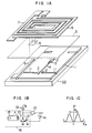
- Fig. 1A is a scheme illustrating an example of an embodiment of the present invention.
- a washer-shaped inductance is used as a SQUID inductance.
- the inductance due to the deep cut off in the Josephson junction can be removed from the SQUID inductance.
- a first high temperature superconductor layer 1 is formed on a substrate 22. Then an aperture portion 3 and a slit 4, where the magnetic flux is coupled, which constitute the SQUID inductance, are formed by processing the first high temperature superconductor layer 1. Further there are disposed deeply cut off portions 11 on both the sides of the slit 4 at the end portion thereof to form Josephson junctions 2. Since microbridge type Josephson junctions are used often in connection with the coherence length of the crystalline grain boundary in the high temperature superconductor, the present invention will be explained below, taking the microbridge type junction as an example.
- a first interlayer insulating layer 5 is formed on this first superconductor layer 1. Further a modulation coil 6 and an input coil 7 are formed by processing a second high temperature superconductor layer thereon. One end of the input coil 7 is taken out by a lower connection electrode 9 through a contact hole formed in the first interlayer insulating layer 5.
- Fig. 1B shows an example of the circuit, in the case where the SQUID is operated as a fluxmeter.
- a constant current power supply 12, a sensor coil 15 and a phase detector amplifier 13 are connected with the SQUID 10.
- Fig. 1C shows a periodically voltage generated, when the SQUID 10 is biased with a constant current and a magnetic flux is applied thereto.
- the high temperature superconductor is made of a mixture of some of oxides of potassium K, calcium Ca, cesium Cs, scandium Sc, strontium Sr, yttrium Y, rare earth elements, barium Ba, copper Cu, thallium Tl, lead Pb, and bismuth Bi.
- YBa2Cu3O 7-x for which T c 90K
- Bi a Sr b Ca c Cu d O x for which T c 100K
- this SQUID fluxmeter utilizes a high temperature superconductor, it can be used at the neighborhood of the liquid nitrogen temperature 77K.
- An insulating substrate is used as th substrate 22.
- magnesium oxide MgO, strontium titanate SrTiO3, etc. are used. It is tried also to use Si or SiO2 for the substrate 22.
- the SQUID inductance should be chosen in a range between 10 and 40 pH and more preferably between 13 and 30 pH.
- the length d of one side of the aperture should be chosen in a range between 6.4 and 25.5 ⁇ m and more preferably between 8.3 and 19.1 ⁇ m.
- the SQUID is constructed by superposing the first high temperature superconductor layer and the second high temperature superconductor layer (forming the modulation coil, etc.) on each other in the form of a double layer as the high temperature superconductor layer.
- the connection electrode 9 and the first high temperature superconductor layer 1 for the SQUID are located on the same plane so that a SQUID element having the simplest structure is realized.
- the superconductor layer 1 is about 1 ⁇ m thick; the interlayer insulating layer 5 is about 1.2 ⁇ m thick; and the modulation coil is about 1.4 ⁇ m thick. From the reason of the fabrication, among the first superconductor layer 1, the interlayer insulating layer 5 and the modulation coil 6 obtained by processing the second superconductor layer, a higher superposed layer is somewhat thicker than a lower layer.
- Fig. 2 is a scheme of an embodiment, in which the SQUID comprises 3 high temperature superconductor layers.
- An aperture portion 3 and a slit 4 are formed by processing a first high temperature superconductor layer 1, which constitute a SQUID inductance. Further two Josephson junction 2 are disposed.
- An interlayer insulating layer 5 is formed thereon and further a connection electrode 17 and an interlayer insulating layer 16 are superposed thereon.
- a modulation coil 6 and an input coil 7 are formed to construct the SQUID.
- Fig. 3 and 4 are a scheme and a plan view illustrating an embodiment, in which a SQUID is constructed by using 2 high temperature superconductor layers. They show the structure of lower layers, removing a part of the input coil 7 and the modulation coil 6. Two sets of apertures 3 and slits 4 are formed by processing the high temperature superconductor layer 1. Two Josephson junction 2 are formed at the central portion and a connection electrode 18 is connected through a contact hole 8 after having insulated them by means of an interlayer insulating layer 5. In this way two of the SQUID inductances used in Figs. 1 and 2 are connected in parallel and thus the inductance is reduced to a half.
- Fig. 5 is a plan view of an embodiment, in which a SQUID is constructed by using two high temperature superconductor layers. Two sets of apertures 3 and slits 4 are formed by processing the high temperature superconductor layer 1. Two Josephson elements are formed at the central portion and a connection electrode 18 is connected through a contact hole 8 after having insulated them by means of an interlayer insulating layer 5.
- a connection electrode 18 is connected through a contact hole 8 after having insulated them by means of an interlayer insulating layer 5.
- two SQUID inductances are connected in parallel. However, evan if more than two inductances are connected in parallel, a similar effect can be obtained. Further, even if a three-layered superconductor layer is used, as indicated in Fig. 2, a similar effect can be obtained.
- Fig. 6A is a plan view of an embodiment, in which a SQUID is constructed by using two high temperature superconductor layers. Two sets of apertures 3 and slits 4 are formed by processing the high temperature superconductor layer 1. A Josephson junction 2 is formed at the extremity portion of each of the slits 4 and a connection electrode 18 is connected through contract holes 8 after having insulated them by means of an interlayer insulating layer 5.
- the inductance is reduced to a half in this embodiment, too, by connecting SQUID inductances in parallel, the difference thereof from the embodiment indicated in Figs. 4 and 5 consists in that the slits 4 are formed in an L-shaped and that the superconductor layer 1 is S-shaped, as indicated in Fig. 6B.
- the superconductor layer 1 is S-shaped, the currents at the places where the magnetic flux is coupled with the two right and left SQUID inductances are compensated, as indicated by arrows. In this way an effect can be obtained that it is possible to nullify magnetic flux noise coming from the exterior.
- the input coils 7 are directed opposite to each other so that the signals from the input coils are not compensated. In this embodiment, too, the SQUID inductance can be reduced and an effect that the optimum operating range can be set is obtained.
- Fig. 7 is a plan view of an embodiment, in which a SQUID is constructed by using a two high temperature superconductor layers. Two sets of apertures 3 and slits 4 are formed by processing the high temperature superconductor layer 1 and 2 SQUID inductances are connected in parallel so that the value of the inductance is reduced to a half and the optimum operating range is set. Further the left and right SQUID inductances are directed opposite to each other so that the magnetic flux noises coupled therewith are compensated. In this way, apart from the effects that the optimum operating range can be set and that the magnetic flux noises are compensated, an effect that the stray capacitance is reduced by making the electrode at the neighborhood of the connection electrode 18 smaller.
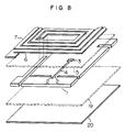
- Fig. 8 is a scheme illustrating still another embodiment, in which a SQUID is constructed by using three high temperature superconductor layers.
- a high temperature superconductor layer serves as a superconducting ground plane.
- an aperture portion 3 and a slit 4 are formed by processing another high temperature layer 1, which constitute a SQUID inductance and two Josephson junctions 2 are disposed.
- an input coil 7 and a modulation coil 6 are formed to constitute the SQUID.
- the SQUID inductance is superposed on the superconducting ground plane, an effect is obtained that the inductance is reduced and the optimum operating range of the SQUID can be realized.
- Fig. 9 is a plan view of a still another embodiment, in which a SQUID is constructed by using two high temperature superconductor layers.
- Four sets of aperture portions 3 and slits 4 are formed by processing the high temperature superconductor layer 1 and 4 SQUID inductances are connected in parallel so that the value of the inductance is reduced to a quarter and the SQUID is set in the optimum operating range. Further these SQUID inductances are directed differently so that magnetic flux noises coupled therewith are compensated. In this way an effect that the optimum operating range can be set and the output voltage is high is obtained. In addition, there is another effect that the SQUID thus constructed is hardly influenced by external magnetic flux noise.
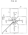
- Fig. 10 is a plan view of still another embodiment, in which a SQUID is constructed by using two high temperature superconductor layers.
- Four sets of aperture portions 3 and slits 4 by processing the high temperature superconductor layers 1 and 4 SQUID inductances are connected in parallel so that the value of the inductance is reduced to a quarter and the SQUID is set in the optimum operating range. Further these SQUID inductances are so combined that magnetic flux noises coupled therewith are compensated. Further the area of the connection electrode 21, which is in the second layer, is made small to reduce stray capacitance.
- Fig. 11 is a scheme of still another embodiment, in which a SQUID is constructed by using two substrates, each of which is provided with a high temperature superconductor layer. An aperture portion 3 and a slit 4 are formed by processing a high temperature superconductor layer 1 disposed on the substrate 21. On the other hand another high temperature superconductor layer is formed on the other substrate and a modulation coil 6 and an input coil are formed by processing it. These two substrates are closely stuck through an interlayer insulating layer to form a SQUID.
- the interlayer insulating layer 5 may be formed on either one of the substrates. In this way an effect can be obtained that the SQUID using high temperature superconductor layers is constructed in a simple manner.
- the Josephson junction used in the above embodiments may be a bridge type junction, in which the stripe width or the layer thickness of the superconductor layers is small, a sandwich type junction or a procimity effect type junction.
- the present invention it is possible to realize a SQUID of excellent characteristics by setting the SQUID inductance at the optimum value to set the signal voltage value at a level sufficiently higher than the thermal noise level in a SQUID using a high temperature superconductor.
- the SQUID can be operated at the liquid nitrogen temperature and therefore very weak magnetic field measurement such as living body magnetism measurement, etc. is facilitated.
Landscapes
- Physics & Mathematics (AREA)
- Condensed Matter Physics & Semiconductors (AREA)
- General Physics & Mathematics (AREA)
- Superconductor Devices And Manufacturing Methods Thereof (AREA)
- Measuring Magnetic Variables (AREA)
Claims (14)
- Interféromètre quantique supraconducteur (SQUID) comprenant :
au moins un substrat (21, 22);
une première couche supraconductrice à haute température (1) pour l'inductance supraconductrice formée sur ledit substrat (21, 22) et possédant au moins une ouverture (3), au moins une fente (4) s'étendant à partir de ladite ouverture (3) dans l'entourage de cette dernière, et deux jonctions de Josephson disposées des deux côtés de ladite fente (4);
une première couche isolante intercalaire (5) formée sur ladite première couche supraconductrice à haute température (1); et
une bobine de modulation (6) et une bobine d'entrée (7) formées au moyen du traitement d'une seconde couche supraconductrice à haute température pour le câblage formée sur ladite première couche isolante (5);
la valeur de l'inductance supraconductrice étant choisie dans une gamme comprise entre 10 et 40 pH. - Interféromètre quantique supraconducteur (SQUID) selon la revendication 1, dans lequel la valeur de l'inductance supraconductrice est choisie dans une gamme comprise entre 13 et 30 pH.
- Interféromètre quantique supraconducteur (SQUID) selon la revendication 1, dans lequel ladite première couche supraconductrice à haute température (1) possède au moins une ouverture carrée (3) et la longueur d'un côté de ladite ouverture est choisie dans une gamme comprise entre 6,4 µm et 25,5 µm.
- Interféromètre quantique supraconducteur (SQUID) selon la revendication 1, dans lequel ladite première couche supraconductrice à haute température (1) possède n (n ≧ 2) ouvertures (3), une fente (4) s'étendant à partir de chacune desdites ouvertures (3) et deux jonctions de Josephson (2) disposées des deux côtés de ladite fente (4), des inductances supraconductrices desdites jonctions étant branchées en parallèle.
- Interféromètre quantique supraconducteur (SQUID) selon la revendication selon la revendication 4, dans lequel la capacité parasite est réduite par réduction de la surface de la partie située au voisinage d'une électrode, qui est située en regard desdites jonctions de Josephson (2).
- Interféromètre quantique supraconducteur (SQUID) selon la revendication 4, dans lequel il est prévu n = 2 ouvertures, et 2 inductances supraconductrices sont branchées en parallèle.
- Interféromètre quantique supraconducteur (SQUID) selon la revendication 4, dans lequel il est prévu n = 4 ouvertures et 4 inductances supraconductrices sont branchées en parallèle.
- Interféromètre quantique supraconducteur (SQUID) selon la revendication 6, dans lequel l'inductance supraconductrice possède une forme de S.
- Interféromètre quantique supraconducteur (SQUID) selon la revendication 7, dans lequel l'inductance supraconductrice recoupe une forme de S à angle droit.
- Interféromètre quantique supraconducteur (SQUID) selon la revendication 1, dans lequel des électrodes de connexion (9) et ladite première couche supraconductrice à haute température (1) sont formées dans le même plan.
- Interféromètre quantique supraconducteur (SQUID) selon la revendication 1, dans lequel en dehors de ladite première couche supraconductrice à haute température (1), de ladite première couche isolante (5) et de ladite seconde couche supraconductrice à haute température, au moins une autre couche supraconductrice à haute température et au moins une autre couche isolante intercalaire sont superposées, et des bornes de ladite bobine d'entrée (7) sont ressorties.
- Interféromètre quantique supraconducteur (SQUID) selon la revendication 1, dans lequel en dehors de ladite première couche supraconductrice à haute température (1), de ladite première couche isolante (5) et de ladite seconde couche supraconductrice à haute température, au moins une autre couche supraconductrice à haute température (20) et au moins une autre couche isolante intercalaire sont superposées, et il est prévu un plan de masse.
- Interféromètre quantique supraconducteur (SQUID) selon la revendication 1, dans lequel il est prévu deux substrats (22), sur l'un desquels ladite première couche supraconductrice à haute température (1) comportant l'ouverture (3) et la fente (4) est formée, et sur l'autre desquels ladite seconde couche supraconductrice à haute température est superposée, ladite bobine de modulation (6) et ladite bobine d'entrée (7) étant formées à partir de ces deux substrats, lesdits deux substrats (21, 22) étant appliqués étroitement l'un contre l'autre moyennant l'interposition de ladite première couche isolante (5).
- Interféromètre quantique supraconducteur (SQUID) selon la revendication 1, dans lequel lesdites couches supraconductrices à haute température (1, 6, 7, 20) sont formées par un mélange de certains oxydes de potassium K, de calcium Ca, de césium Cs, de scandium Sc, de strontium Sr, d'yttrium Y, d'éléments des terres rares, de baryum Ba, de cuivre Cu, de thallium Tl, de plomb Pb et de bismuth Bi.
Applications Claiming Priority (2)
| Application Number | Priority Date | Filing Date | Title |
|---|---|---|---|
| JP63023669A JP2749048B2 (ja) | 1988-02-05 | 1988-02-05 | 超電導量子干渉計 |
| JP23669/88 | 1988-02-05 |
Publications (3)
| Publication Number | Publication Date |
|---|---|
| EP0327123A2 EP0327123A2 (fr) | 1989-08-09 |
| EP0327123A3 EP0327123A3 (en) | 1989-12-13 |
| EP0327123B1 true EP0327123B1 (fr) | 1993-07-28 |
Family
ID=12116895
Family Applications (1)
| Application Number | Title | Priority Date | Filing Date |
|---|---|---|---|
| EP19890101953 Expired - Lifetime EP0327123B1 (fr) | 1988-02-05 | 1989-02-03 | Squid |
Country Status (3)
| Country | Link |
|---|---|
| EP (1) | EP0327123B1 (fr) |
| JP (1) | JP2749048B2 (fr) |
| DE (1) | DE68907737T2 (fr) |
Cited By (1)
| Publication number | Priority date | Publication date | Assignee | Title |
|---|---|---|---|---|
| DE112012005382B4 (de) | 2011-12-21 | 2023-06-15 | Superconducting Sensor Technology Corporation | Hochtemperatur-Supraleiter-Magnet-Sensor |
Families Citing this family (10)
| Publication number | Priority date | Publication date | Assignee | Title |
|---|---|---|---|---|
| WO1992019978A1 (fr) * | 1987-05-11 | 1992-11-12 | Datalight Limited | Spectometres rmn/rqn portables |
| JP2893714B2 (ja) * | 1989-05-25 | 1999-05-24 | 株式会社日立製作所 | 薄膜型squid磁束計およびこれを用いた生体磁気計測装置 |
| JPH042979A (ja) * | 1990-04-19 | 1992-01-07 | Seiko Instr Inc | 高感度磁場検出器 |
| US5053834A (en) * | 1990-08-31 | 1991-10-01 | Quantum Magnetics, Inc. | High symmetry dc SQUID system |
| JPH05297089A (ja) * | 1992-04-20 | 1993-11-12 | Sumitomo Electric Ind Ltd | 磁気センサ |
| AU5126493A (en) * | 1993-09-07 | 1995-03-27 | Conductus, Inc. | Improved squid coupling structure |
| US5600243A (en) * | 1993-09-07 | 1997-02-04 | Conductus, Inc. | Magnetically shielded magnetic sensor with squid and ground plane |
| JPH07191113A (ja) * | 1993-12-27 | 1995-07-28 | Chodendo Sensor Kenkyusho:Kk | Squid磁気センサ |
| DE19513481A1 (de) * | 1995-04-13 | 1996-10-17 | Forschungszentrum Juelich Gmbh | HF-SQUID-Gradiometer mit resonanter Flußfokussierungsstruktur |
| FI102695B (fi) * | 1996-06-11 | 1999-01-29 | Nanoway Oy | CB-Tunnelointiin perustuva lämpömittari |
Family Cites Families (4)
| Publication number | Priority date | Publication date | Assignee | Title |
|---|---|---|---|---|
| JPS59148890A (ja) * | 1983-02-15 | 1984-08-25 | Mitsubishi Electric Corp | センサ−用磁気結合回路 |
| JPS61196587A (ja) * | 1985-02-26 | 1986-08-30 | Mitsubishi Electric Corp | 直流駆動型超伝導量子干渉素子 |
| DE3769201D1 (de) * | 1986-05-21 | 1991-05-16 | Siemens Ag | Squid-magnetometer fuer eine vorrichtung zur messung schwacher magnetfelder. |
| JPS6370089U (fr) * | 1986-10-28 | 1988-05-11 |
-
1988
- 1988-02-05 JP JP63023669A patent/JP2749048B2/ja not_active Expired - Lifetime
-
1989
- 1989-02-03 EP EP19890101953 patent/EP0327123B1/fr not_active Expired - Lifetime
- 1989-02-03 DE DE1989607737 patent/DE68907737T2/de not_active Expired - Fee Related
Cited By (1)
| Publication number | Priority date | Publication date | Assignee | Title |
|---|---|---|---|---|
| DE112012005382B4 (de) | 2011-12-21 | 2023-06-15 | Superconducting Sensor Technology Corporation | Hochtemperatur-Supraleiter-Magnet-Sensor |
Also Published As
| Publication number | Publication date |
|---|---|
| DE68907737D1 (de) | 1993-09-02 |
| EP0327123A2 (fr) | 1989-08-09 |
| EP0327123A3 (en) | 1989-12-13 |
| JP2749048B2 (ja) | 1998-05-13 |
| JPH01200679A (ja) | 1989-08-11 |
| DE68907737T2 (de) | 1993-11-11 |
Similar Documents
| Publication | Publication Date | Title |
|---|---|---|
| US5218297A (en) | Superconductive quantum interference device in high temperature environments having reduced inductance and improved thermal noise response | |
| EP0545948B1 (fr) | Systeme de squid (dispositif d'interference quantique supraconducteur) a courant continu, ayant une tres grande symetrie | |
| US5767043A (en) | Multiple squid direct signal injection device formed on a single layer substrate | |
| US5656937A (en) | Low-noise symmetric dc SQUID system having two pairs of washer coils and a pair of Josephson junctions connected in series | |
| CN102460196B (zh) | 用于测量时变磁场或磁场梯度的测量仪器、电阻元件和测量系统 | |
| US5574290A (en) | Superconducting quantum interference device | |
| US4585999A (en) | Radiofrequency amplifier based on a dc superconducting quantum interference device | |
| EP1547167B1 (fr) | Dispositif supraconducteur a interferences quantiques | |
| EP0567386A2 (fr) | Capteur de magnétisme planaire utilisant un interféromètre quantique à supraconducteur à oxyde | |
| US8781542B2 (en) | High-temperature superconducting magnetic sensor and fabrication method of the same | |
| EP0327123B1 (fr) | Squid | |
| US5625290A (en) | Complex superconducting quantum interference device and circuit | |
| US5955400A (en) | SQUID integrated with pickup coils | |
| Kaczmarek et al. | Advanced HTS DC SQUIDs with step-edge Josephson junctions for geophysical applications | |
| Granata et al. | Improved superconducting quantum interference device magnetometer for low cross talk operation | |
| US6323645B1 (en) | Superconducting quantum interference device | |
| JPH07235700A (ja) | 超伝導超格子結晶デバイス | |
| JPH05299711A (ja) | Squid | |
| JP2879010B2 (ja) | 超電導素子 | |
| Yamasaki et al. | Design and fabrication of multichannel dc SQUIDs for biomagnetic applications | |
| Testa et al. | Performance of asymmetric superconducting quantum interference devices | |
| JPH08186300A (ja) | 酸化物squid用ピックアップコイル | |
| JP2943293B2 (ja) | Dc―squid磁力計 | |
| JPH08316536A (ja) | 超電導装置 | |
| Ketchen | Low Noise Dc Squids for the 1990S |
Legal Events
| Date | Code | Title | Description |
|---|---|---|---|
| PUAI | Public reference made under article 153(3) epc to a published international application that has entered the european phase |
Free format text: ORIGINAL CODE: 0009012 |
|
| AK | Designated contracting states |
Kind code of ref document: A2 Designated state(s): DE FR GB |
|
| PUAL | Search report despatched |
Free format text: ORIGINAL CODE: 0009013 |
|
| AK | Designated contracting states |
Kind code of ref document: A3 Designated state(s): DE FR GB |
|
| 17P | Request for examination filed |
Effective date: 19900529 |
|
| 17Q | First examination report despatched |
Effective date: 19920910 |
|
| GRAA | (expected) grant |
Free format text: ORIGINAL CODE: 0009210 |
|
| AK | Designated contracting states |
Kind code of ref document: B1 Designated state(s): DE FR GB |
|
| REF | Corresponds to: |
Ref document number: 68907737 Country of ref document: DE Date of ref document: 19930902 |
|
| ET | Fr: translation filed | ||
| PGFP | Annual fee paid to national office [announced via postgrant information from national office to epo] |
Ref country code: FR Payment date: 19931216 Year of fee payment: 6 |
|
| PLBE | No opposition filed within time limit |
Free format text: ORIGINAL CODE: 0009261 |
|
| STAA | Information on the status of an ep patent application or granted ep patent |
Free format text: STATUS: NO OPPOSITION FILED WITHIN TIME LIMIT |
|
| 26N | No opposition filed | ||
| PG25 | Lapsed in a contracting state [announced via postgrant information from national office to epo] |
Ref country code: FR Effective date: 19951031 |
|
| REG | Reference to a national code |
Ref country code: FR Ref legal event code: ST |
|
| PGFP | Annual fee paid to national office [announced via postgrant information from national office to epo] |
Ref country code: DE Payment date: 19960425 Year of fee payment: 8 |
|
| PGFP | Annual fee paid to national office [announced via postgrant information from national office to epo] |
Ref country code: GB Payment date: 19970124 Year of fee payment: 9 |
|
| PG25 | Lapsed in a contracting state [announced via postgrant information from national office to epo] |
Ref country code: DE Effective date: 19971101 |
|
| PG25 | Lapsed in a contracting state [announced via postgrant information from national office to epo] |
Ref country code: GB Free format text: LAPSE BECAUSE OF NON-PAYMENT OF DUE FEES Effective date: 19980203 |
|
| GBPC | Gb: european patent ceased through non-payment of renewal fee |
Effective date: 19980203 |