EP0327152A1 - Verfahren zum Herstellen einer Halbleiteranordnung, wobei auf selbstregistrierende Art und Weise Metallsilicid angebracht wird - Google Patents
Verfahren zum Herstellen einer Halbleiteranordnung, wobei auf selbstregistrierende Art und Weise Metallsilicid angebracht wird Download PDFInfo
- Publication number
- EP0327152A1 EP0327152A1 EP89200132A EP89200132A EP0327152A1 EP 0327152 A1 EP0327152 A1 EP 0327152A1 EP 89200132 A EP89200132 A EP 89200132A EP 89200132 A EP89200132 A EP 89200132A EP 0327152 A1 EP0327152 A1 EP 0327152A1
- Authority
- EP
- European Patent Office
- Prior art keywords
- layer
- gate electrode
- silicon
- mask
- polycrystalline silicon
- Prior art date
- Legal status (The legal status is an assumption and is not a legal conclusion. Google has not performed a legal analysis and makes no representation as to the accuracy of the status listed.)
- Granted
Links
Images

Classifications
-
- H—ELECTRICITY
- H10—SEMICONDUCTOR DEVICES; ELECTRIC SOLID-STATE DEVICES NOT OTHERWISE PROVIDED FOR
- H10D—INORGANIC ELECTRIC SEMICONDUCTOR DEVICES
- H10D30/00—Field-effect transistors [FET]
- H10D30/01—Manufacture or treatment
- H10D30/021—Manufacture or treatment of FETs having insulated gates [IGFET]
- H10D30/0223—Manufacture or treatment of FETs having insulated gates [IGFET] having source and drain regions or source and drain extensions self-aligned to sides of the gate
- H10D30/0227—Manufacture or treatment of FETs having insulated gates [IGFET] having source and drain regions or source and drain extensions self-aligned to sides of the gate having both lightly-doped source and drain extensions and source and drain regions self-aligned to the sides of the gate, e.g. lightly-doped drain [LDD] MOSFET or double-diffused drain [DDD] MOSFET
-
- H—ELECTRICITY
- H10—SEMICONDUCTOR DEVICES; ELECTRIC SOLID-STATE DEVICES NOT OTHERWISE PROVIDED FOR
- H10D—INORGANIC ELECTRIC SEMICONDUCTOR DEVICES
- H10D30/00—Field-effect transistors [FET]
- H10D30/60—Insulated-gate field-effect transistors [IGFET]
- H10D30/67—Thin-film transistors [TFT]
- H10D30/674—Thin-film transistors [TFT] characterised by the active materials
- H10D30/6741—Group IV materials, e.g. germanium or silicon carbide
- H10D30/6743—Silicon
- H10D30/6745—Polycrystalline or microcrystalline silicon
-
- H—ELECTRICITY
- H10—SEMICONDUCTOR DEVICES; ELECTRIC SOLID-STATE DEVICES NOT OTHERWISE PROVIDED FOR
- H10D—INORGANIC ELECTRIC SEMICONDUCTOR DEVICES
- H10D30/00—Field-effect transistors [FET]
- H10D30/01—Manufacture or treatment
- H10D30/021—Manufacture or treatment of FETs having insulated gates [IGFET]
- H10D30/0212—Manufacture or treatment of FETs having insulated gates [IGFET] using self-aligned silicidation
-
- H—ELECTRICITY
- H10—SEMICONDUCTOR DEVICES; ELECTRIC SOLID-STATE DEVICES NOT OTHERWISE PROVIDED FOR
- H10D—INORGANIC ELECTRIC SEMICONDUCTOR DEVICES
- H10D30/00—Field-effect transistors [FET]
- H10D30/60—Insulated-gate field-effect transistors [IGFET]
- H10D30/67—Thin-film transistors [TFT]
- H10D30/6704—Thin-film transistors [TFT] having supplementary regions or layers in the thin films or in the insulated bulk substrates for controlling properties of the device
- H10D30/6713—Thin-film transistors [TFT] having supplementary regions or layers in the thin films or in the insulated bulk substrates for controlling properties of the device characterised by the properties of the source or drain regions, e.g. compositions or sectional shapes
-
- H—ELECTRICITY
- H10—SEMICONDUCTOR DEVICES; ELECTRIC SOLID-STATE DEVICES NOT OTHERWISE PROVIDED FOR
- H10D—INORGANIC ELECTRIC SEMICONDUCTOR DEVICES
- H10D64/00—Electrodes of devices having potential barriers
- H10D64/01—Manufacture or treatment
- H10D64/021—Manufacture or treatment using multiple gate spacer layers, e.g. bilayered sidewall spacers
-
- H—ELECTRICITY
- H10—SEMICONDUCTOR DEVICES; ELECTRIC SOLID-STATE DEVICES NOT OTHERWISE PROVIDED FOR
- H10P—GENERIC PROCESSES OR APPARATUS FOR THE MANUFACTURE OR TREATMENT OF DEVICES COVERED BY CLASS H10
- H10P14/00—Formation of materials, e.g. in the shape of layers or pillars
- H10P14/60—Formation of materials, e.g. in the shape of layers or pillars of insulating materials
- H10P14/63—Formation of materials, e.g. in the shape of layers or pillars of insulating materials characterised by the formation processes
- H10P14/6302—Non-deposition formation processes
- H10P14/6316—Formation by nitridation, e.g. nitridation of the substrate
-
- H—ELECTRICITY
- H10—SEMICONDUCTOR DEVICES; ELECTRIC SOLID-STATE DEVICES NOT OTHERWISE PROVIDED FOR
- H10P—GENERIC PROCESSES OR APPARATUS FOR THE MANUFACTURE OR TREATMENT OF DEVICES COVERED BY CLASS H10
- H10P32/00—Diffusion of dopants within, into or out of wafers, substrates or parts of devices
- H10P32/30—Diffusion for doping of conductive or resistive layers
- H10P32/302—Doping polycrystalline silicon or amorphous silicon layers
-
- H—ELECTRICITY
- H10—SEMICONDUCTOR DEVICES; ELECTRIC SOLID-STATE DEVICES NOT OTHERWISE PROVIDED FOR
- H10P—GENERIC PROCESSES OR APPARATUS FOR THE MANUFACTURE OR TREATMENT OF DEVICES COVERED BY CLASS H10
- H10P50/00—Etching of wafers, substrates or parts of devices
- H10P50/71—Etching of wafers, substrates or parts of devices using masks for conductive or resistive materials
-
- H—ELECTRICITY
- H10—SEMICONDUCTOR DEVICES; ELECTRIC SOLID-STATE DEVICES NOT OTHERWISE PROVIDED FOR
- H10P—GENERIC PROCESSES OR APPARATUS FOR THE MANUFACTURE OR TREATMENT OF DEVICES COVERED BY CLASS H10
- H10P95/00—Generic processes or apparatus for manufacture or treatments not covered by the other groups of this subclass
- H10P95/90—Thermal treatments, e.g. annealing or sintering
-
- Y—GENERAL TAGGING OF NEW TECHNOLOGICAL DEVELOPMENTS; GENERAL TAGGING OF CROSS-SECTIONAL TECHNOLOGIES SPANNING OVER SEVERAL SECTIONS OF THE IPC; TECHNICAL SUBJECTS COVERED BY FORMER USPC CROSS-REFERENCE ART COLLECTIONS [XRACs] AND DIGESTS
- Y10—TECHNICAL SUBJECTS COVERED BY FORMER USPC
- Y10S—TECHNICAL SUBJECTS COVERED BY FORMER USPC CROSS-REFERENCE ART COLLECTIONS [XRACs] AND DIGESTS
- Y10S148/00—Metal treatment
- Y10S148/147—Silicides
Definitions
- the invention relates to a method of manufacturing a semiconductor device comprising an insulated gate field effect transistor, in which a surface of a semiconductor substrate of monocrystalline silicon is provided with a layer of silicon oxide, on which a gate electrode is formed by covering the layer of silicon oxide with a layer of doped polycrystalline silicon, which, after an etching mask has been provided, is subjected to an etching treatment, after which, using the gate electrode as a mask, source and drain zones are formed by ion implantation in the semiconductor substrate, the gate electrode is provided with edge isolation parts by covering the surface with a layer of silicon oxide and by then subjecting it to an anisotropic etching treatment, the polycrystalline silicon of the gate electrode and the monocrystalline silicon of the source and drain zones are exposed, the surface is covered with a metal-containing layer, the substrate is subjected to a heat treatment, in which a metal silicide is formed by reaction of the metal-containing layer with underlying mono- and polycrystalline silicon, and parts of the metal-containing layer not coverted into metal silicide
- the metal-containing layer reacts with the monocrystalline silicon of the source and drain zones and with the polycrystalline silicon of the gate electrode, which results in a metal silicide being formed
- a reaction does not occur between the metal-containing layer and silicon oxide.
- Parts of the metal containing layer present above the edge isolation parts of the gate electrode are then not converted into metal silicide. These parts can be etched away without the metal silicide formed being attacked in practice.
- the source and drain zones and the gate electrode are provided in a self-registered manner with a top layer of metal silicide. Due to this top layer, the source and drain zones can be contacted at a comparatively low resistance and the gate electrode has a comparatively low resistance.
- US-PS No. 4,477,310 discloses a methd of the kind mentioned in the opening paragraph, in which during the formation of the gate electrode in the layer of doped polycrystalline silicon an etching mask of photoresist is used.
- the invention has inter alia for its object to provide a method, by which the said disadvantages are obviated.
- the method of the kind mentioned in the opening paragraph is for this purpose characterized in that during the formation of the gate electrode in the layer of polycrystalline silicon a mask containing a silicon nitride is used as an etching mask. It has been found that with the use of an etching mask containing silicon nitride the gate electrode can be realized with substantially straight side edges which extend substantially transversely to the surface of the semiconductor substrate. As a result, such edge isolation parts can be provided in a simple manner on the gate electrode that during the formation of metal silicide the risk of shortcircuit of source and drain zones and gate electrode is practically avoided.
- a layer containing silicon nitride moreover has the advantages that the etching mask prevents oxidation of the underlying polycrystalline silicon and that the etching mask can be etched away selectively with respect to the monocrystalline silicon of the source and drain zones, the polycrystalline silicon of the gate electrode and the silicon oxide of the edge isolation parts.
- the method according to the invention is characterized in that the etching mask containing silicon nitride is not removed until the source and drain zones are formed.
- the monocrystalline silicon must be protected. This is effected very efficaciously by a layer silicon oxide formed by thermal oxidation on the monocrystalline silicon. Defects formed during the implantation in the crystal lattice can be removed efficaciously after the implantation by a heat treatment carried out in oxygen. During such oxidation treatments, the gate electrode is covered on its upper side by the mask of material containing silicon nitride, as a result of which oxidation of the gate electrode on its upper side is prevented.
- the mask containing silicon nitride may be a mask which is formed in the top layer of the layer of polycrystalline silicon, which is converted by nitridation or by an ion implantation at least in part into silicon nitride.
- the mask may also be formed in a layer of silicon oxynitride.
- a mask of silicon nitride is used as mask containing silicon nitride.
- a mask of silicon nitride provides optimum protection from oxidation and can be etched away very selectively with respect to silicon and silicon oxide.
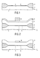
- the substrate 1 is now heated for 30 minutes in dry oxygen, while a thin layer of silicon oxide 6 having a thickness of about 20 nm is formed on its surface 5.
- a gate electrode 11 is formed on the layer of silicon oxide 6 by covering the layer 6 with a layer 7 of polycrystalline silicon doped with about 1020 phosphorus atoms/cm3 and having a thickness of about 500 nm, which is subjected, after an etching mask 10 has been provided, to an etching treatment.
- a mask containing silicon nitride is used as etching mask 10. This mask is formed by covering the layer of polycrystalline silicon 7 in a usual manner with a layer of silicon nitride 8 having a thickness of about 150 nm. In a usual manner, whilst masking with a photoresist mask 9, the etching mask 10 is formed therein by a plasma etching treatment with fluorine ions.
- Such an etching mask containing silicon nitride may also be formed in different ways, for example in a layer of silicon oxynitride or in a top layer of the layer of polycrystalline silicon 7, which is converted by implantation of nitrogen ions at least in part into silicon nitride.
- the etching mask 10 is formed in the manner described above.
- a layer of silicon oxide having, for example, a thickness of about 15 nm is preferably provided between the two layers. This layer, which is not shown in the drawings, may be obtained by oxidation of the layer of polycrystalline silicon 7.
- the gate electrode 11 Whilst masking with the etching mask 10, which according to the invention is a mask containing silicon nitride, the gate electrode 11 is now formed by a plasma etching treatment with chlorine ions. It has been found that a gate electrode 11 can thus be obtained having practically straight side edges 12, which extend practically transversely to the surface 5. As will appear from the following description, such edge isolation parts 20 can thus be provided in a simple manner on the gate electrode 11 that during the formation of metal silicide the risk of shortcircuits is very small.
- the use of silicon nitride for the etching mask 10 moreover has the advantage that the etching mask 10 prevents oxidation of the underlying polycrystalline silicon and that the etching mask can be etched away selectively with respect to monocrystalline silicon, polycrystalline silicon and silicon oxide.
- an ion implantation indicated diagrammatically by arrows 15 is carried out, in which, whilst masking the gate electrode 11 and the field oxide regions 3, ions designated by reference numeral 16 are implanted into the semiconductor region 4.
- ions designated by reference numeral 16 are implanted into the semiconductor region 4.
- phosphorus ions at an energy of 50 keV and a dose of 1013 ions/cm2 are implanted.
- the substrate is heated for about 40 minutes to about 925°C in dry oxygen.
- Silicon oxide layers 13 are then formed on the uncovered side edges 12 of the gate electrode 11 and the parts 14 of the layer of silicon oxide 6, which are located between the gate electrode 11 and the field oxide regions 3, obtain thickness of about 35 nm.
- semiconductor zones 17 and 18 are formed. These zones constitute the source and drain zones of the field effect transistor.
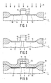
- the gate electrode 11 is provided with edge isolation parts 20 by covering the surface 5 with a layer of silicon oxide 19 having a thickness of about 300 nm, by heating the substrate to a temperature of 700°C in a gas mixture containing tetraethyl orthosilicate and by then subjecting it to an anisotropic etching treatment with reactive ions. This etching treatment is stopped when the oxide has been removed from the monocrystalline silicon of the semiconductor zones 17 and 18.
- the substrate 1 is now heated again for about 40 minutes to about 925°C in dry oxygen.
- the layers of silicon oxide 21 having a thickness of about 25 nm located above the semiconductor zones 17 and 18 are then formed. These parts 21 protect the semiconductor region 4 again during an ion implantation indicated diagrammatically by arrows 22.
- the edge isolation parts 20 and the field oxide regions 3 are now implanted into the semiconductor region 4. In this case, these ions are arsenic ions at an energy of 50 keV and a dose of 1015 ions/cm2.
- the mask 10 (with the layer of silicon oxide possibly located under it), and the layers of silicon oxide 21 are etched away, or in other words: the polycrystalline silicon of the gate electrode 11 and the monocrystalline silicon of the connection zones are exposed.
- the substrate 1 is now covered by a metal-containing layer 26, such as, for example, a layer of titanium. Subsequently, the substrate 1 is subjected for about 10 seconds to a heat treatment at a temperature of about 650°C in a nitrogen atmosphere. The metal-containing layer 26 then reacts with underlying silicon 11, 24, 25, but it does not react with underlying silicon oxide 3, 20.
- a nitridized titanium layer is formed, which can then be etched away selectively in a solution of ammonia and hydrogen peroxide.
- the gate electrode 11 and the zones 24 and 25 are provided in a self-registered manner with a top layer 27, the source and drain zones 17 and 18 can be contacted at a comparatively low resistance and the gate electrode 11 with the associated top layer has a comparatively low resistance.
- the etching mask 10 containing silicon nitride is removed only after the source and drain zones 17 and 18 and the associated connection zones 24 and 25 have been formed. This, it is avoided that during the formation of the oxide layers 14 and 21 the gate electrode 11 oxidizes on its upper side. If this were not the case, about 150 nm of oxide would have been formed on the polycrystalline silicon during the heat treatments in which about 60 nm of silicon oxide in all has been formed on the monocrystalline silicon. Polycrystalline silicon doped with phosphorus oxidizes in dry oxygen much more rapidly than monocrystalline silicon. Both kinds of silicon oxide are attacked at a substantially equal rate by etchants, however.
- the gate electrode 11 were not covered with the mask 10 of silicon nitride, 150 nm of silicon oxide would have to be etched away before the metal-containing layer 26 could be provided. Now that the gate electrode according to the invention is covered with the mask 10, however, only 60 nm of silicon oxide need be removed. Thus. it is avoided that the field oxide regions 3 and the edge isolation parts 20 are etched for an unnecessarily long time during the process of exposing the zones 24 and 25 and the gate electrode 11. Especially edges 28 of the field oxide regions 3 could be attacked to such an extent that the pn junctions between the connection zones 24 and 25 and the semiconductor region 4 could be exposed. These junctions would then be shortcircuited by metal silicide. This risk is greater if the said pn junction extends in close proximity of the surface 5, which is the case especially with transistors having submicron dimensions.
- a gate electrode 11 can be obtained with straight side edges 12 directed transversely to the surface.
- the edge isolation regions 20 then have a thickness which is larger than if the side edges should extend obliquely to the surface. This would have been the case if the gate electrode would have been formed directly with a photoresist mask (and not with the intermediary of the mask 10 of silicon nitride). Due to the large thickness of the side isolation parts 20, the risk of shortcircuit between the top layers of metal silicide 27 is a minimum.
Landscapes
- Insulated Gate Type Field-Effect Transistor (AREA)
- Electrodes Of Semiconductors (AREA)
Applications Claiming Priority (2)
| Application Number | Priority Date | Filing Date | Title |
|---|---|---|---|
| NL8800222A NL8800222A (nl) | 1988-01-29 | 1988-01-29 | Werkwijze voor het vervaardigen van een halfgeleiderinrichting waarbij op zelfregistrerende wijze metaalsilicide wordt aangebracht. |
| NL8800222 | 1988-01-29 |
Publications (2)
| Publication Number | Publication Date |
|---|---|
| EP0327152A1 true EP0327152A1 (de) | 1989-08-09 |
| EP0327152B1 EP0327152B1 (de) | 1993-11-24 |
Family
ID=19851680
Family Applications (1)
| Application Number | Title | Priority Date | Filing Date |
|---|---|---|---|
| EP89200132A Expired - Lifetime EP0327152B1 (de) | 1988-01-29 | 1989-01-24 | Verfahren zum Herstellen einer Halbleiteranordnung, wobei auf selbstregistrierende Art und Weise Metallsilicid angebracht wird |
Country Status (6)
| Country | Link |
|---|---|
| US (1) | US4885259A (de) |
| EP (1) | EP0327152B1 (de) |
| JP (1) | JPH025435A (de) |
| KR (1) | KR890012402A (de) |
| DE (1) | DE68910841T2 (de) |
| NL (1) | NL8800222A (de) |
Cited By (2)
| Publication number | Priority date | Publication date | Assignee | Title |
|---|---|---|---|---|
| WO2004021429A1 (en) * | 2002-08-29 | 2004-03-11 | Micron Technology, Inc. | Transistor structure including a metal silicide gate and channel implants and method of manufacturing the same |
| CN101987985A (zh) * | 2009-08-04 | 2011-03-23 | 财团法人工业技术研究院 | 一种组合物及其用途 |
Families Citing this family (40)
| Publication number | Priority date | Publication date | Assignee | Title |
|---|---|---|---|---|
| JP3437863B2 (ja) | 1993-01-18 | 2003-08-18 | 株式会社半導体エネルギー研究所 | Mis型半導体装置の作製方法 |
| US20010008288A1 (en) * | 1988-01-08 | 2001-07-19 | Hitachi, Ltd. | Semiconductor integrated circuit device having memory cells |
| US5374576A (en) * | 1988-12-21 | 1994-12-20 | Hitachi, Ltd. | Method of fabricating stacked capacitor cell memory devices |
| US5153145A (en) * | 1989-10-17 | 1992-10-06 | At&T Bell Laboratories | Fet with gate spacer |
| US5306655A (en) * | 1990-07-24 | 1994-04-26 | Matsushita Electric Industrial Co., Ltd. | Structure and method of manufacture for MOS field effect transistor having lightly doped drain and source diffusion regions |
| JPH04217373A (ja) * | 1990-12-18 | 1992-08-07 | Sharp Corp | 不揮発性記憶装置およびその製造方法 |
| JP3061891B2 (ja) * | 1991-06-21 | 2000-07-10 | キヤノン株式会社 | 半導体装置の製造方法 |
| KR960000225B1 (ko) * | 1991-08-26 | 1996-01-03 | 가부시키가이샤 한도오따이 에네루기 겐큐쇼 | 절연게이트형 반도체장치의 제작방법 |
| JP2997123B2 (ja) * | 1992-04-03 | 2000-01-11 | 株式会社東芝 | 半導体装置の製造方法 |
| US5411907A (en) * | 1992-09-01 | 1995-05-02 | Taiwan Semiconductor Manufacturing Company | Capping free metal silicide integrated process |
| JPH06140396A (ja) * | 1992-10-23 | 1994-05-20 | Yamaha Corp | 半導体装置とその製法 |
| KR0140464B1 (ko) * | 1993-08-26 | 1998-07-15 | 세끼자와 다다시 | 실리사이드 전극을 갖는 반도체장치의 제조방법 |
| TW297142B (de) | 1993-09-20 | 1997-02-01 | Handotai Energy Kenkyusho Kk | |
| US6777763B1 (en) * | 1993-10-01 | 2004-08-17 | Semiconductor Energy Laboratory Co., Ltd. | Semiconductor device and method for fabricating the same |
| JP3030368B2 (ja) | 1993-10-01 | 2000-04-10 | 株式会社半導体エネルギー研究所 | 半導体装置およびその作製方法 |
| US5438006A (en) * | 1994-01-03 | 1995-08-01 | At&T Corp. | Method of fabricating gate stack having a reduced height |
| JPH07263684A (ja) * | 1994-03-25 | 1995-10-13 | Mitsubishi Electric Corp | 電界効果トランジスタの製造方法 |
| US6200871B1 (en) * | 1994-08-30 | 2001-03-13 | Texas Instruments Incorporated | High performance self-aligned silicide process for sub-half-micron semiconductor technologies |
| FR2734402B1 (fr) * | 1995-05-15 | 1997-07-18 | Brouquet Pierre | Procede pour l'isolement electrique en micro-electronique, applicable aux cavites etroites, par depot d'oxyde a l'etat visqueux et dispositif correspondant |
| US5858844A (en) * | 1995-06-07 | 1999-01-12 | Advanced Micro Devices, Inc. | Method for construction and fabrication of submicron field-effect transistors by optimization of poly oxide process |
| US6393495B1 (en) | 1995-11-21 | 2002-05-21 | Diamond Multimedia Systems, Inc. | Modular virtualizing device driver architecture |
| US6289396B1 (en) | 1995-11-21 | 2001-09-11 | Diamond Multimedia Systems, Inc. | Dynamic programmable mode switching device driver architecture |
| US6009476A (en) * | 1995-11-21 | 1999-12-28 | Diamond Multimedia Systems, Inc. | Device driver architecture supporting emulation environment |
| US5752032A (en) * | 1995-11-21 | 1998-05-12 | Diamond Multimedia Systems, Inc. | Adaptive device driver using controller hardware sub-element identifier |
| KR100206878B1 (ko) * | 1995-12-29 | 1999-07-01 | 구본준 | 반도체소자 제조방법 |
| JPH104092A (ja) * | 1996-06-14 | 1998-01-06 | Nec Corp | 半導体装置の製造方法 |
| US5705417A (en) * | 1996-06-19 | 1998-01-06 | Vanguard International Semiconductor Corporation | Method for forming self-aligned silicide structure |
| US5691212A (en) * | 1996-09-27 | 1997-11-25 | Taiwan Semiconductor Manufacturing Company, Ltd. | MOS device structure and integration method |
| US5753557A (en) * | 1996-10-07 | 1998-05-19 | Vanguard International Semiconductor Company | Bridge-free self aligned silicide process |
| US5744395A (en) * | 1996-10-16 | 1998-04-28 | Taiwan Semiconductor Manufacturing Company, Ltd. | Low resistance, self-aligned, titanium silicide structures, using a single rapid thermal anneal procedure |
| US5783486A (en) * | 1996-10-18 | 1998-07-21 | Vanguard International Semiconductor Corporation | Bridge-free self aligned silicide process |
| TW346652B (en) * | 1996-11-09 | 1998-12-01 | Winbond Electronics Corp | Semiconductor production process |
| US6013569A (en) * | 1997-07-07 | 2000-01-11 | United Microelectronics Corp. | One step salicide process without bridging |
| US6603180B1 (en) * | 1997-11-28 | 2003-08-05 | Advanced Micro Devices, Inc. | Semiconductor device having large-area silicide layer and process of fabrication thereof |
| US6015736A (en) * | 1997-12-19 | 2000-01-18 | Advanced Micro Devices, Inc. | Method and system for gate stack reoxidation control |
| US5895244A (en) * | 1998-01-08 | 1999-04-20 | Texas Instruments - Acer Incorporated | Process to fabricate ultra-short channel nMOSFETs with self-aligned silicide contact |
| US6995053B2 (en) * | 2004-04-23 | 2006-02-07 | Sharp Laboratories Of America, Inc. | Vertical thin film transistor |
| WO2005006429A1 (de) * | 2003-07-08 | 2005-01-20 | Infineon Technologies Ag | Integrierte schaltungsanordnung mit niederohmigen kontakten und herstellungsverfahren |
| JP2006237453A (ja) * | 2005-02-28 | 2006-09-07 | Toshiba Corp | 半導体装置及びその製造方法 |
| US8741704B2 (en) | 2012-03-08 | 2014-06-03 | International Business Machines Corporation | Metal oxide semiconductor (MOS) device with locally thickened gate oxide |
Citations (4)
| Publication number | Priority date | Publication date | Assignee | Title |
|---|---|---|---|---|
| EP0066097A2 (de) * | 1981-05-29 | 1982-12-08 | Texas Instruments Incorporated | Silizid-Kontakte für CMOS-Anordnungen |
| US4587718A (en) * | 1984-11-30 | 1986-05-13 | Texas Instruments Incorporated | Process for forming TiSi2 layers of differing thicknesses in a single integrated circuit |
| US4587710A (en) * | 1984-06-15 | 1986-05-13 | Gould Inc. | Method of fabricating a Schottky barrier field effect transistor |
| GB2172743A (en) * | 1985-03-23 | 1986-09-24 | Stc Plc | Forming gate sidewall oxide spacers |
Family Cites Families (11)
| Publication number | Priority date | Publication date | Assignee | Title |
|---|---|---|---|---|
| NL7510903A (nl) * | 1975-09-17 | 1977-03-21 | Philips Nv | Werkwijze voor het vervaardigen van een halfgelei- derinrichting, en inrichting vervaardigd volgens de werkwijze. |
| US4441247A (en) * | 1981-06-29 | 1984-04-10 | Intel Corporation | Method of making MOS device by forming self-aligned polysilicon and tungsten composite gate |
| JPS58154270A (ja) * | 1982-03-09 | 1983-09-13 | Toshiba Corp | 半導体装置の製造方法 |
| JPS59188974A (ja) * | 1983-04-11 | 1984-10-26 | Nec Corp | 半導体装置の製造方法 |
| US4477310A (en) * | 1983-08-12 | 1984-10-16 | Tektronix, Inc. | Process for manufacturing MOS integrated circuit with improved method of forming refractory metal silicide areas |
| SE453547B (sv) * | 1985-03-07 | 1988-02-08 | Stiftelsen Inst Mikrovags | Forfarande vid framstellning av integrerade kretsar der pa en substratplatta ledare och s k gate-strukturer uppbygges |
| US4663191A (en) * | 1985-10-25 | 1987-05-05 | International Business Machines Corporation | Salicide process for forming low sheet resistance doped silicon junctions |
| US4703551A (en) * | 1986-01-24 | 1987-11-03 | Ncr Corporation | Process for forming LDD MOS/CMOS structures |
| US4818715A (en) * | 1987-07-09 | 1989-04-04 | Industrial Technology Research Institute | Method of fabricating a LDDFET with self-aligned silicide |
| US4755478A (en) * | 1987-08-13 | 1988-07-05 | International Business Machines Corporation | Method of forming metal-strapped polysilicon gate electrode for FET device |
| US4786609A (en) * | 1987-10-05 | 1988-11-22 | North American Philips Corporation, Signetics Division | Method of fabricating field-effect transistor utilizing improved gate sidewall spacers |
-
1988
- 1988-01-29 NL NL8800222A patent/NL8800222A/nl not_active Application Discontinuation
- 1988-12-28 US US07/290,923 patent/US4885259A/en not_active Expired - Fee Related
-
1989
- 1989-01-24 EP EP89200132A patent/EP0327152B1/de not_active Expired - Lifetime
- 1989-01-24 DE DE68910841T patent/DE68910841T2/de not_active Expired - Fee Related
- 1989-01-26 KR KR1019890000787A patent/KR890012402A/ko not_active Ceased
- 1989-01-27 JP JP1016502A patent/JPH025435A/ja active Pending
Patent Citations (4)
| Publication number | Priority date | Publication date | Assignee | Title |
|---|---|---|---|---|
| EP0066097A2 (de) * | 1981-05-29 | 1982-12-08 | Texas Instruments Incorporated | Silizid-Kontakte für CMOS-Anordnungen |
| US4587710A (en) * | 1984-06-15 | 1986-05-13 | Gould Inc. | Method of fabricating a Schottky barrier field effect transistor |
| US4587718A (en) * | 1984-11-30 | 1986-05-13 | Texas Instruments Incorporated | Process for forming TiSi2 layers of differing thicknesses in a single integrated circuit |
| GB2172743A (en) * | 1985-03-23 | 1986-09-24 | Stc Plc | Forming gate sidewall oxide spacers |
Cited By (7)
| Publication number | Priority date | Publication date | Assignee | Title |
|---|---|---|---|---|
| WO2004021429A1 (en) * | 2002-08-29 | 2004-03-11 | Micron Technology, Inc. | Transistor structure including a metal silicide gate and channel implants and method of manufacturing the same |
| US6821855B2 (en) | 2002-08-29 | 2004-11-23 | Micron Technology, Inc. | Reverse metal process for creating a metal silicide transistor gate structure |
| US7067880B2 (en) | 2002-08-29 | 2006-06-27 | Micron Technology, Inc. | Transistor gate structure |
| US7288817B2 (en) | 2002-08-29 | 2007-10-30 | Micron Technology, Inc. | Reverse metal process for creating a metal silicide transistor gate structure |
| US7601598B2 (en) | 2002-08-29 | 2009-10-13 | Micron Technology, Inc. | Reverse metal process for creating a metal silicide transistor gate structure |
| CN101987985A (zh) * | 2009-08-04 | 2011-03-23 | 财团法人工业技术研究院 | 一种组合物及其用途 |
| CN101987985B (zh) * | 2009-08-04 | 2013-05-22 | 财团法人工业技术研究院 | 一种组合物及其用途 |
Also Published As
| Publication number | Publication date |
|---|---|
| NL8800222A (nl) | 1989-08-16 |
| US4885259A (en) | 1989-12-05 |
| DE68910841T2 (de) | 1994-05-19 |
| JPH025435A (ja) | 1990-01-10 |
| DE68910841D1 (de) | 1994-01-05 |
| KR890012402A (ko) | 1989-08-26 |
| EP0327152B1 (de) | 1993-11-24 |
Similar Documents
| Publication | Publication Date | Title |
|---|---|---|
| EP0327152B1 (de) | Verfahren zum Herstellen einer Halbleiteranordnung, wobei auf selbstregistrierende Art und Weise Metallsilicid angebracht wird | |
| US4512073A (en) | Method of forming self-aligned contact openings | |
| US5780350A (en) | MOSFET device with improved LDD region and method of making same | |
| KR970000703B1 (ko) | 반도체 장치의 제조 방법 | |
| EP0631308A2 (de) | Verfahren zum Steuern der Dicke des Gate-Oxyds für die Herstellung von Halbleiterbauelementen | |
| JPH11283935A (ja) | 半導体装置の製造方法 | |
| US4502894A (en) | Method of fabricating polycrystalline silicon resistors in integrated circuit structures using outdiffusion | |
| JP3505493B2 (ja) | 半導体装置の製造方法 | |
| JP3165051B2 (ja) | 半導体素子のウェル形成方法 | |
| US5763316A (en) | Substrate isolation process to minimize junction leakage | |
| US5851909A (en) | Method of producing semiconductor device using an adsorption layer | |
| JP2948486B2 (ja) | 半導体素子の製造方法 | |
| US6153456A (en) | Method of selectively applying dopants to an integrated circuit semiconductor device without using a mask | |
| JP3293987B2 (ja) | 半導体装置の製造方法 | |
| JP2843037B2 (ja) | 半導体装置の製造方法 | |
| US6133122A (en) | Method of fabricating semiconductor device for preventing rising-up of siliside | |
| JPH02153525A (ja) | 半導体装置の製造方法 | |
| JPH05102074A (ja) | Mosトランジスタ | |
| JP3050190B2 (ja) | 半導体装置の製造方法 | |
| KR0161732B1 (ko) | 반도체소자의 콘택 제조방법 | |
| JP2525186B2 (ja) | 半導体装置の製造方法 | |
| JPS6010717A (ja) | 半導体装置用コンタクトの形成方法 | |
| JPS6161268B2 (de) | ||
| JP3311082B2 (ja) | 半導体装置の製造方法 | |
| JP2774019B2 (ja) | 半導体装置の製造方法 |
Legal Events
| Date | Code | Title | Description |
|---|---|---|---|
| PUAI | Public reference made under article 153(3) epc to a published international application that has entered the european phase |
Free format text: ORIGINAL CODE: 0009012 |
|
| AK | Designated contracting states |
Kind code of ref document: A1 Designated state(s): DE FR GB IT NL |
|
| 17P | Request for examination filed |
Effective date: 19900207 |
|
| 17Q | First examination report despatched |
Effective date: 19910829 |
|
| GRAA | (expected) grant |
Free format text: ORIGINAL CODE: 0009210 |
|
| AK | Designated contracting states |
Kind code of ref document: B1 Designated state(s): DE FR GB IT NL |
|
| PG25 | Lapsed in a contracting state [announced via postgrant information from national office to epo] |
Ref country code: NL Effective date: 19931124 |
|
| PGFP | Annual fee paid to national office [announced via postgrant information from national office to epo] |
Ref country code: GB Payment date: 19931230 Year of fee payment: 6 |
|
| REF | Corresponds to: |
Ref document number: 68910841 Country of ref document: DE Date of ref document: 19940105 |
|
| ITF | It: translation for a ep patent filed | ||
| PGFP | Annual fee paid to national office [announced via postgrant information from national office to epo] |
Ref country code: FR Payment date: 19940126 Year of fee payment: 6 |
|
| ET | Fr: translation filed | ||
| PGFP | Annual fee paid to national office [announced via postgrant information from national office to epo] |
Ref country code: DE Payment date: 19940330 Year of fee payment: 6 |
|
| NLV1 | Nl: lapsed or annulled due to failure to fulfill the requirements of art. 29p and 29m of the patents act | ||
| PLBE | No opposition filed within time limit |
Free format text: ORIGINAL CODE: 0009261 |
|
| STAA | Information on the status of an ep patent application or granted ep patent |
Free format text: STATUS: NO OPPOSITION FILED WITHIN TIME LIMIT |
|
| 26N | No opposition filed | ||
| PG25 | Lapsed in a contracting state [announced via postgrant information from national office to epo] |
Ref country code: GB Effective date: 19950124 |
|
| ITPR | It: changes in ownership of a european patent |
Owner name: CAMBIO RAGIONE SOCIALE;PHILIPS ELECTRONICS N.V. |
|
| GBPC | Gb: european patent ceased through non-payment of renewal fee |
Effective date: 19950124 |
|
| PG25 | Lapsed in a contracting state [announced via postgrant information from national office to epo] |
Ref country code: FR Effective date: 19950929 |
|
| PG25 | Lapsed in a contracting state [announced via postgrant information from national office to epo] |
Ref country code: DE Effective date: 19951003 |
|
| REG | Reference to a national code |
Ref country code: FR Ref legal event code: ST |
|
| PG25 | Lapsed in a contracting state [announced via postgrant information from national office to epo] |
Ref country code: IT Free format text: LAPSE BECAUSE OF NON-PAYMENT OF DUE FEES;WARNING: LAPSES OF ITALIAN PATENTS WITH EFFECTIVE DATE BEFORE 2007 MAY HAVE OCCURRED AT ANY TIME BEFORE 2007. THE CORRECT EFFECTIVE DATE MAY BE DIFFERENT FROM THE ONE RECORDED. Effective date: 20050124 |