EP0327392A2 - Dispositif d'affichage à cristal liquide - Google Patents
Dispositif d'affichage à cristal liquide Download PDFInfo
- Publication number
- EP0327392A2 EP0327392A2 EP89301090A EP89301090A EP0327392A2 EP 0327392 A2 EP0327392 A2 EP 0327392A2 EP 89301090 A EP89301090 A EP 89301090A EP 89301090 A EP89301090 A EP 89301090A EP 0327392 A2 EP0327392 A2 EP 0327392A2
- Authority
- EP
- European Patent Office
- Prior art keywords
- liquid crystal
- transparent
- light
- scanning electrodes
- crystal display
- Prior art date
- Legal status (The legal status is an assumption and is not a legal conclusion. Google has not performed a legal analysis and makes no representation as to the accuracy of the status listed.)
- Granted
Links
- 239000004973 liquid crystal related substance Substances 0.000 title claims abstract description 45
- 239000011159 matrix material Substances 0.000 claims description 23
- 239000000758 substrate Substances 0.000 claims description 23
- 239000004988 Nematic liquid crystal Substances 0.000 claims description 2
- 238000005401 electroluminescence Methods 0.000 claims description 2
- 239000005262 ferroelectric liquid crystals (FLCs) Substances 0.000 description 10
- 230000007423 decrease Effects 0.000 description 3
- 239000011521 glass Substances 0.000 description 2
- 238000007789 sealing Methods 0.000 description 2
- 210000002858 crystal cell Anatomy 0.000 description 1
- 238000002474 experimental method Methods 0.000 description 1
- 238000012986 modification Methods 0.000 description 1
- 230000004048 modification Effects 0.000 description 1
Images




Classifications
-
- G—PHYSICS
- G09—EDUCATION; CRYPTOGRAPHY; DISPLAY; ADVERTISING; SEALS
- G09G—ARRANGEMENTS OR CIRCUITS FOR CONTROL OF INDICATING DEVICES USING STATIC MEANS TO PRESENT VARIABLE INFORMATION
- G09G3/00—Control arrangements or circuits, of interest only in connection with visual indicators other than cathode-ray tubes
- G09G3/20—Control arrangements or circuits, of interest only in connection with visual indicators other than cathode-ray tubes for presentation of an assembly of a number of characters, e.g. a page, by composing the assembly by combination of individual elements arranged in a matrix no fixed position being assigned to or needed to be assigned to the individual characters or partial characters
- G09G3/34—Control arrangements or circuits, of interest only in connection with visual indicators other than cathode-ray tubes for presentation of an assembly of a number of characters, e.g. a page, by composing the assembly by combination of individual elements arranged in a matrix no fixed position being assigned to or needed to be assigned to the individual characters or partial characters by control of light from an independent source
- G09G3/3406—Control of illumination source
- G09G3/342—Control of illumination source using several illumination sources separately controlled corresponding to different display panel areas, e.g. along one dimension such as lines
-
- G—PHYSICS
- G02—OPTICS
- G02F—OPTICAL DEVICES OR ARRANGEMENTS FOR THE CONTROL OF LIGHT BY MODIFICATION OF THE OPTICAL PROPERTIES OF THE MEDIA OF THE ELEMENTS INVOLVED THEREIN; NON-LINEAR OPTICS; FREQUENCY-CHANGING OF LIGHT; OPTICAL LOGIC ELEMENTS; OPTICAL ANALOGUE/DIGITAL CONVERTERS
- G02F1/00—Devices or arrangements for the control of the intensity, colour, phase, polarisation or direction of light arriving from an independent light source, e.g. switching, gating or modulating; Non-linear optics
- G02F1/01—Devices or arrangements for the control of the intensity, colour, phase, polarisation or direction of light arriving from an independent light source, e.g. switching, gating or modulating; Non-linear optics for the control of the intensity, phase, polarisation or colour
- G02F1/13—Devices or arrangements for the control of the intensity, colour, phase, polarisation or direction of light arriving from an independent light source, e.g. switching, gating or modulating; Non-linear optics for the control of the intensity, phase, polarisation or colour based on liquid crystals, e.g. single liquid crystal display cells
- G02F1/133—Constructional arrangements; Operation of liquid crystal cells; Circuit arrangements
- G02F1/1333—Constructional arrangements; Manufacturing methods
- G02F1/1347—Arrangement of liquid crystal layers or cells in which the final condition of one light beam is achieved by the addition of the effects of two or more layers or cells
- G02F1/13476—Arrangement of liquid crystal layers or cells in which the final condition of one light beam is achieved by the addition of the effects of two or more layers or cells in which at least one liquid crystal cell or layer assumes a scattering state
-
- G—PHYSICS
- G02—OPTICS
- G02F—OPTICAL DEVICES OR ARRANGEMENTS FOR THE CONTROL OF LIGHT BY MODIFICATION OF THE OPTICAL PROPERTIES OF THE MEDIA OF THE ELEMENTS INVOLVED THEREIN; NON-LINEAR OPTICS; FREQUENCY-CHANGING OF LIGHT; OPTICAL LOGIC ELEMENTS; OPTICAL ANALOGUE/DIGITAL CONVERTERS
- G02F1/00—Devices or arrangements for the control of the intensity, colour, phase, polarisation or direction of light arriving from an independent light source, e.g. switching, gating or modulating; Non-linear optics
- G02F1/01—Devices or arrangements for the control of the intensity, colour, phase, polarisation or direction of light arriving from an independent light source, e.g. switching, gating or modulating; Non-linear optics for the control of the intensity, phase, polarisation or colour
- G02F1/13—Devices or arrangements for the control of the intensity, colour, phase, polarisation or direction of light arriving from an independent light source, e.g. switching, gating or modulating; Non-linear optics for the control of the intensity, phase, polarisation or colour based on liquid crystals, e.g. single liquid crystal display cells
- G02F1/133—Constructional arrangements; Operation of liquid crystal cells; Circuit arrangements
- G02F1/1333—Constructional arrangements; Manufacturing methods
- G02F1/1335—Structural association of cells with optical devices, e.g. polarisers or reflectors
- G02F1/1336—Illuminating devices
-
- G—PHYSICS
- G02—OPTICS
- G02F—OPTICAL DEVICES OR ARRANGEMENTS FOR THE CONTROL OF LIGHT BY MODIFICATION OF THE OPTICAL PROPERTIES OF THE MEDIA OF THE ELEMENTS INVOLVED THEREIN; NON-LINEAR OPTICS; FREQUENCY-CHANGING OF LIGHT; OPTICAL LOGIC ELEMENTS; OPTICAL ANALOGUE/DIGITAL CONVERTERS
- G02F1/00—Devices or arrangements for the control of the intensity, colour, phase, polarisation or direction of light arriving from an independent light source, e.g. switching, gating or modulating; Non-linear optics
- G02F1/01—Devices or arrangements for the control of the intensity, colour, phase, polarisation or direction of light arriving from an independent light source, e.g. switching, gating or modulating; Non-linear optics for the control of the intensity, phase, polarisation or colour
- G02F1/13—Devices or arrangements for the control of the intensity, colour, phase, polarisation or direction of light arriving from an independent light source, e.g. switching, gating or modulating; Non-linear optics for the control of the intensity, phase, polarisation or colour based on liquid crystals, e.g. single liquid crystal display cells
- G02F1/133—Constructional arrangements; Operation of liquid crystal cells; Circuit arrangements
- G02F1/1333—Constructional arrangements; Manufacturing methods
- G02F1/1347—Arrangement of liquid crystal layers or cells in which the final condition of one light beam is achieved by the addition of the effects of two or more layers or cells
- G02F1/13471—Arrangement of liquid crystal layers or cells in which the final condition of one light beam is achieved by the addition of the effects of two or more layers or cells in which all the liquid crystal cells or layers remain transparent, e.g. FLC, ECB, DAP, HAN, TN, STN, SBE-LC cells
-
- G—PHYSICS
- G09—EDUCATION; CRYPTOGRAPHY; DISPLAY; ADVERTISING; SEALS
- G09G—ARRANGEMENTS OR CIRCUITS FOR CONTROL OF INDICATING DEVICES USING STATIC MEANS TO PRESENT VARIABLE INFORMATION
- G09G2310/00—Command of the display device
- G09G2310/02—Addressing, scanning or driving the display screen or processing steps related thereto
- G09G2310/0237—Switching ON and OFF the backlight within one frame
Definitions
- the present invention relates to a liquid crystal display device, and more particularly, to a light transmissive type ferroelectric liquid crystal display device having a matrix type display panel.
- Figs. 7 and 8 show fundamental structures of a conventional matrix type display with use of a light transmissive type ferroelectric liquid crystal display.
- polarizers 1 and 9 arranged to have crossed Nicols relation are formed oppositely to each other, and a light source (not shown) is arranged on the outer surface of the polarizer 9.
- Transparent substrates 2 and 8 of glass are arranged on the inner surfaces of the polarizers 1 and 9, respectively.
- Sixteen transparent conductive scanning electrodes 4 (L1 to L16) having a strip shape are formed in parallel with each other on the inner surface of the transparent substrate 2, and sixteen transparent conductive signal electrodes 7 for applying a signal having a strip shape are formed in parallel with each other on the inner surface of the transparent substrate 8.
- a ferroelectric liquid crystal layer 5 is formed between the transparent substrates 2 and 8 and is sealed by a sealing element 6.
- Respective drivers 3 are connected to the respective scanning electrodes 4 (L1 to L16) so as to apply a voltage Vc thereto.
- Respective drivers 10 are connected to the respective signal electrodes 7 so as to apply a voltage Vs thereto.
- the positive voltage V0 Vc - Vs must be applied thereto for ⁇ 0 seconds. That is, it takes at least 2 ⁇ 0 seconds to rewrite the picture elements defined on one scanning electrode 4.
- the aforementioned switching operation between the positive and negative voltages is referred to the selection of the scanning electrode 4 hereinafter, and the time interval necessary for the aforementioned switching operation is referred to the time interval for selecting the scanning electrode 4.
- the voltages Vth1, -Vth2 and ⁇ 0 are determined in accordance with the kinds of the ferroelectric liquid crystal to be used.
- T F M ⁇ 2 ⁇ 0 (3) wherein M is a positive integer.
- the frame period T F is 0.08 seconds.
- a matrix type ferroelectric liquid crystal display device further comprising a back light source 11 as shown in Fig. 9 in addition to the structure shown in Fig. 8 is proposed.
- the back light source 11 is arranged on the outer surface of the polarizer 9, and the light intensity thereof is controlled by a control circuit 12 periodically as shown in (a) of Fig. 10. While the light intensity of the back light source 11 is kept relatively low, the control circuit 12 controls the drivers 3 and 10 so as to select individual scanning electrodes 4 sequentially.
- the back light source 11 when at least one picture element is rewritten, the back light source 11 is turned off so that the whole matrix display panel becomes relatively dark. On the other hand, except for the respective time intervals for rewriting the picture elements, the back light source 11 is turned on.
- the aforementioned conventional display device shown in Fig. 9 can prevent the display from flickering certainly.
- the scanning electrode 4 can not be selected for the time interval when the light intensity of the back light source 11 is kept relatively high, the frame period T F increases. If the ratio of the time interval for the high light intensity to the time interval for the low light intensity of the back light source 11 is 1 : 1, the frame period T F becomes twice as long as that in the aforementioned display device not having the back light source. In the case that the time interval ⁇ 0 is 100 micro seconds and the number M of the scanning electrodes 4 is 400 as described above, the frame period T F becomes 0.16 seconds, resulting in that the movement of the images becomes slow in a moving image display.
- An essential object of the present invention is to provide a liquid crystal display device which is able to prevent the display from flicking thereon in a relatively short frame period T F .
- a liquid crystal display device comprising: first and second transparent substrates arranged in parallel to each other with a predetermined interval; a plurality of transparent scanning electrodes formed on the inner surface of said first transparent substrate; a plurality of transparent signal electrodes formed on the inner surface of said second transparent substrate so as to cross said transparent scanning electrodes; a liquid crystal layer for displaying picture elements defined at the crossings between said transparent scanning electrodes and said transparent signal electrodes in accordance with a predetermined voltage applied thereto, said liquid crystal layer being arranged between said first transparent substrate and said second transparent substrate; a light source for emitting a light toward said liquid crystal layer; and a light shutter means arranged between said liquid crystal layer and said light source for shading the light incident to the picture elements being rewritten from said light source.
- the frame period T F does not increase, resulting in that the quality of images displayed on the liquid crystal display device can be improved.
- Figs. 1 and 2 show fundamental structures of a two dimensional matrix type liquid crystal display device of the preferred embodiment according to the present invention.
- a light shutter panel 21 is inserted between a matrix display panel 20 and a light source 19.
- the structures of the light shutter panel 21 and the light source 19 are substantially same as those shown in Fig. 9.
- the light shutter panel 21 is comprised of a liquid crystal cell having a sandwich structure of two transparent substrates 13 and 15 of glass and a ferroelectric liquid crystal layer 5a contained therebetween in a sealed state by a sealing member 6a. Between the light shutter panel 21 and the light source 19, a polarizer 16 is inserted so as to satisfy a crossed Nicols relation with the polarizer 9 of the matrix display panel 20.
- sixteen transparent scanning electrodes 4a are formed on the inner surface of the substrate 13 so as to correspond to the scanning electrodes 4 of the matrix display panel 20, and on the opposed inner surface of the substrate 15, a transparent rectangular ground electrode 14 is formed so as to cover the whole area of the substrate 15.
- These sixteen scanning electrodes 4a (L1 a to L16 a ) are divided into four groups, each being comprised of successive four scanning electrodes L 1a to L 4a , L 5a to L 8a , L 9a to L 12a , L 13a to L 16a , respectively, and each scanning electrode belonging to one group is connected to a driver 17 so as to be able to apply a voltage Vh commonly. Further, a ground driver 18 is connected to the ground electrode 14 in order to give zero voltage to the same.
- the light shutter panel 21 can shade the light from the light source 19 in the unit of each group when the voltage Vh is applied thereto by the corresponding driver 17 (D1, D2, D3 or D4).
- the shutter panel 21 has four shutter elements in this example.
- a frequency for driving the drivers D1 to D4 is chosen higher than that of the commercial electric power in order to avoid possible flickers.
- the light intensity of the light source 19 is kept constant as shown in Fig. 6.
- a control circuit 30 applies predetermined voltages to the scanning electrodes 4 (L1 to L16), the signal electrodes 7 and the scanning electrodes 4a (L 1a to L 16a ) through the drivers 3, the drivers 10 and the drivers 17 (D1 to D4), respectively, as described below in detail.
- the matrix display panel 20 has M scanning electrodes 4 to be driven in a frame period T F and that M scanning electrodes 4 are divided into 2 ⁇ N groups from the first to 2N-th, each of which is comprised of successive K scanning electrodes 4, wherein M, N and K are positive integers chosen so as to satisfy the following conditions: N > 60 (Hz) ⁇ T F (4) wherein 60 (Hz) is the frequency of the commercial electric power, and K ⁇ M 2N (5)
- the first condition is given in order to avoid possible flickers.
- K is desirably chosen as a minimum integer among integers satisfying the condition (5).
- the light shutter panel 21 has the same grouping structure as that of the matrix display panel 20 as far as the scanning electrodes 4a are concerned. Namely, it has 2 ⁇ N light shutter elements being comprised of the first to 2N-th groups, each group having K successive scanning electrodes 4a.
- the light amount incident to a picture element defined on an arbitrary scanning electrode 4 decreases for a time interval of T F /2N and increases for the time interval of T F /2N, and this decrease and increase pattern of the light amount is repeated. Namely, the period of the repeated pattern becomes T F /N, and according to the condition (4), the following unequality is satisfied. ⁇ 1 60 (seconds) (6)
- the control circuit 30 applies a voltage Vh satisfying the following equation (7) (or (8)) to the scanning electrodes L 1a a to L 4a through the driver D1 for the time interval ⁇ 0 seconds.
- the control circuit 30 applies a voltage Vh satisfying the following equation (8) (or (7)) to the scanning electrodes L 1a to L 4a through the driver D1 for the time interval ⁇ 0 seconds.
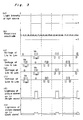
- the drivers D1 to D4 are driven so that the light shutter elements are opened and closed as shown in (c) to (f) of Fig. 6, in synchronizing with that the rewritten electrodes 4 of the matrix display panel 20 are selected as shown in (b) of Fig. 6.
- (c) to (f) of Fig. 3 show the driving voltages applied to the scanning electrodes L 1a to L 4a , L 5a to L 8a , L 9a to L 12a , and L 13a to L 16a in the above case, and also (g) and (h) of Fig. 3 show the lightness of the picture elements defined on the scanning electrode L1 when the picture elements are set in the bright and dark states, respectively, in this case.
- the lightness of the picture elements changes, mainly, according to the switching period of the light shutter.
- a liquid crystal display device having the fundamental structure shown in Figs. 1 and 2 and having the 400 scanning electrodes 4 was made.
- the voltage Vc is applied to the 400 scanning electrodes 4 of the liquid crystal display device, the images with no flicker can be obtained on the liquid crystal display device.
- the scanning electrodes 4 are selected sequentially in the order from the scanning electrode L1 to L16 as shown in (b) of Fig. 6. However, there is no problem even though the light shutter element corresponding to the scanning electrode 4 being far away from the selected scanning electrode 4 is opened.
- the ferroelectric liquid crystal panel 21 is used as the light shutter panel.
- a lighting apparatus having the same effect as that of the ferroelectric liquid crystal panel such as an electroluminescence display, a vacuum fluorescent display, a plasma display panel, and a twisted nematic liquid crystal display, respectively comprising strip shaped picture elements arranged along the scanning electrodes 4 of the matrix display panel 20, can be used as the light shutter panel.
- the light shutter element corresponding to the scanning electrodes L1 to L4 when the light shutter element corresponding to the scanning electrodes L1 to L4 are closed, the light shutter element corresponding to the scanning electrodes L5 to L8 are opened and the light shutter element corresponding to the scanning electrodes L9 to L12 are closed.
- the opened light shutter element and the shut light shutter element alternately at intervals of the aforementioned scanning electrode group.
- the flicker can be preferably suppressed.
- the present invention is not limited to this, the light shutter elements corresponding to the scanning electrodes 4 of the picture elements being rewritten may be closed, and the other light shutter elements may be opened, resulting in that the flicker can be suppressed sufficiently.
- the scanning electrodes 4 corresponds to one light shutter element in the unit of the electrode group, because it is difficult to make the scanning electrodes 4 correspond to the light shutter elements one by one precisely when the matrix display panel 20 is overlapped on the light shutter panel 21.
- the panels 20 and 21 are overlapped with a high precision so that the scanning electrodes 4 correspond to the light shutter elements one by one, respectively, the opening and closing operation of every one light shutter element corresponding to the selected one electrode 4 may be controlled.
- the opening time interval OP of the light shutter elements is smaller than a predetermined time interval.
- the light shutter element corresponding to the scanning electrodes L5 and L8 are closed and the light shutter element corresponding to the scanning electrodes L6 and L7 is opened. Because it is taken into consideration that the light transmitting through the opened light shutter element spreads out when there is a gap between the matrix display panel 20 and the light shutter panel 21. Therefore, in the case that the liquid crystal display device has a structure where the light transmitting through the opened light shutter element does not spread out, the opening time interval OP may not be smaller than the predetermined time interval.
Landscapes
- Physics & Mathematics (AREA)
- Engineering & Computer Science (AREA)
- Nonlinear Science (AREA)
- General Physics & Mathematics (AREA)
- Chemical & Material Sciences (AREA)
- Mathematical Physics (AREA)
- Theoretical Computer Science (AREA)
- Crystallography & Structural Chemistry (AREA)
- Computer Hardware Design (AREA)
- Optics & Photonics (AREA)
- Liquid Crystal Display Device Control (AREA)
- Liquid Crystal (AREA)
- Transforming Electric Information Into Light Information (AREA)
- Control Of Indicators Other Than Cathode Ray Tubes (AREA)
Applications Claiming Priority (2)
| Application Number | Priority Date | Filing Date | Title |
|---|---|---|---|
| JP63024502A JPH01200232A (ja) | 1988-02-04 | 1988-02-04 | 強誘電性液晶表示装置 |
| JP24502/88 | 1988-02-04 |
Publications (3)
| Publication Number | Publication Date |
|---|---|
| EP0327392A2 true EP0327392A2 (fr) | 1989-08-09 |
| EP0327392A3 EP0327392A3 (fr) | 1991-01-09 |
| EP0327392B1 EP0327392B1 (fr) | 1994-04-27 |
Family
ID=12139966
Family Applications (1)
| Application Number | Title | Priority Date | Filing Date |
|---|---|---|---|
| EP89301090A Expired - Lifetime EP0327392B1 (fr) | 1988-02-04 | 1989-02-03 | Dispositif d'affichage à cristal liquide |
Country Status (4)
| Country | Link |
|---|---|
| US (1) | US5103328A (fr) |
| EP (1) | EP0327392B1 (fr) |
| JP (1) | JPH01200232A (fr) |
| DE (1) | DE68914860T2 (fr) |
Cited By (5)
| Publication number | Priority date | Publication date | Assignee | Title |
|---|---|---|---|---|
| EP1030209A3 (fr) * | 1999-02-17 | 2002-01-16 | Siemens Aktiengesellschaft | Dispositif d'affichage à intensité variable |
| WO2002021198A1 (fr) * | 2000-09-11 | 2002-03-14 | Koninklijke Philips Electronics N.V. | Dispositif d'affichage |
| WO2002021042A1 (fr) * | 2000-09-11 | 2002-03-14 | Koninklijke Philips Electronics N.V. | Dispositif d'affichage |
| WO2004079437A1 (fr) * | 2003-03-03 | 2004-09-16 | Koninklijke Philips Electronics N.V. | Dispositif d'affichage et systeme d'eclairage associe |
| CN107548471A (zh) * | 2015-04-27 | 2018-01-05 | 默克专利股份有限公司 | 用于光学切换元件的光学切换层 |
Families Citing this family (40)
| Publication number | Priority date | Publication date | Assignee | Title |
|---|---|---|---|---|
| JP2668600B2 (ja) * | 1990-11-29 | 1997-10-27 | シャープ株式会社 | 液晶表示装置 |
| TW228633B (fr) * | 1991-01-17 | 1994-08-21 | Semiconductor Energy Res Co Ltd | |
| DE69228843T2 (de) * | 1991-05-27 | 1999-08-26 | Dainippon Ink And Chemicals | Flüssigkristallvorrichtung |
| US5251048A (en) * | 1992-05-18 | 1993-10-05 | Kent State University | Method and apparatus for electronic switching of a reflective color display |
| US5359345A (en) * | 1992-08-05 | 1994-10-25 | Cree Research, Inc. | Shuttered and cycled light emitting diode display and method of producing the same |
| US5724062A (en) * | 1992-08-05 | 1998-03-03 | Cree Research, Inc. | High resolution, high brightness light emitting diode display and method and producing the same |
| RU2042973C1 (ru) * | 1992-12-30 | 1995-08-27 | Малое научно-производственное предприятие "ЭЛО" | Жидкокристаллическая цветная дисплейная панель с активной матрицей |
| US5303054A (en) * | 1993-05-17 | 1994-04-12 | Chunghwa Picture Tubes, Ltd. | Line electron beam light source for projection LCD system |
| US5381252A (en) * | 1993-06-22 | 1995-01-10 | Chunghawa Picture Tubes, Ltd. | Opposed scanning electron beams light source for projection LCD |
| US5479187A (en) * | 1994-02-23 | 1995-12-26 | Chunghwa Picture Tubes, Ltd. | Vertically scanned narrow light beam source for LCD display |
| US5592193A (en) * | 1994-03-10 | 1997-01-07 | Chunghwa Picture Tubes, Ltd. | Backlighting arrangement for LCD display panel |
| US6985127B1 (en) | 1994-09-01 | 2006-01-10 | The United States Of America As Represented By The Secretary Of The Navy | Programmable gray-scale liquid crystal display |
| US5812105A (en) * | 1996-06-10 | 1998-09-22 | Cree Research, Inc. | Led dot matrix drive method and apparatus |
| US7385574B1 (en) | 1995-12-29 | 2008-06-10 | Cree, Inc. | True color flat panel display module |
| JP3484702B2 (ja) * | 1996-03-14 | 2004-01-06 | セイコーエプソン株式会社 | 液晶装置及びそれを用いた電子機器 |
| WO1997039378A1 (fr) * | 1996-04-18 | 1997-10-23 | Flat Panel Display Co. (Fpd) B.V. | Unite de visualisation |
| JPH10241572A (ja) * | 1997-02-25 | 1998-09-11 | Fujitsu Ltd | プラズマディスプレイ装置およびプラズマディスプレイパネル |
| US6144359A (en) * | 1998-03-30 | 2000-11-07 | Rockwell Science Center | Liquid crystal displays utilizing polymer dispersed liquid crystal devices for enhanced performance and reduced power |
| JP4519251B2 (ja) * | 1999-10-13 | 2010-08-04 | シャープ株式会社 | 液晶表示装置およびその制御方法 |
| CN1209742C (zh) * | 2000-06-15 | 2005-07-06 | 夏普株式会社 | 液晶显示装置、照明装置和照明装置的驱动方法 |
| JP2002006815A (ja) * | 2000-06-21 | 2002-01-11 | Sony Corp | 液晶表示装置 |
| JP2003050569A (ja) * | 2000-11-30 | 2003-02-21 | Hitachi Ltd | 液晶表示装置 |
| JP4348409B2 (ja) * | 2001-02-27 | 2009-10-21 | ドルビー ラボラトリーズ ライセンシング コーポレイション | 高ダイナミック・レンジ表示装置 |
| US7855708B2 (en) * | 2001-09-05 | 2010-12-21 | Honeywell International Inc. | LED backlight luminance sensing for LCDs |
| KR100432009B1 (ko) * | 2001-12-03 | 2004-05-22 | 주식회사 팬택 | 이동형 정보통신 기기용 양방향 디스플레이형 액정표시장치 |
| US8687271B2 (en) | 2002-03-13 | 2014-04-01 | Dolby Laboratories Licensing Corporation | N-modulation displays and related methods |
| EP2378507B1 (fr) * | 2002-03-13 | 2018-05-09 | Dolby Laboratories Licensing Corporation | Compensation de défaut d'éléments électroluminescents dans un afficheur |
| KR100828531B1 (ko) * | 2002-07-26 | 2008-05-13 | 삼성전자주식회사 | 액정 표시 장치 |
| JP2004144990A (ja) * | 2002-10-24 | 2004-05-20 | Alps Electric Co Ltd | 両面発光型液晶表示モジュール |
| TW200506452A (en) * | 2003-08-11 | 2005-02-16 | Hannstar Display Corp | Liquid crystal display (LCD) having an electro-optical light shutter |
| JP4341398B2 (ja) * | 2003-12-18 | 2009-10-07 | セイコーエプソン株式会社 | 光伝搬特性制御装置、光学表示装置、光伝搬特性制御プログラムおよび光学表示装置制御プログラム、並びに光伝搬特性制御方法および光学表示装置制御方法 |
| US20060256244A1 (en) * | 2004-02-25 | 2006-11-16 | Jak Martin J J | Display device and an illumination system therefor |
| US7349043B2 (en) * | 2004-05-24 | 2008-03-25 | Nec Corporation | Light source, display device, portable terminal device, and ray direction switching element |
| CN101013211B (zh) * | 2006-01-31 | 2010-10-13 | Nec液晶技术株式会社 | 显示设备、终端设备和显示面板 |
| KR100836434B1 (ko) * | 2006-08-17 | 2008-06-09 | 엘지이노텍 주식회사 | 디스플레이 장치 및 이를 이용한 이동통신 단말기 |
| WO2008092276A1 (fr) * | 2007-02-01 | 2008-08-07 | Dolby Laboratories Licensing Corporation | Étalonnage de dispositifs d'affichage à rétroéclairage variable dans l'espace |
| US20090322800A1 (en) | 2008-06-25 | 2009-12-31 | Dolby Laboratories Licensing Corporation | Method and apparatus in various embodiments for hdr implementation in display devices |
| US20100214282A1 (en) | 2009-02-24 | 2010-08-26 | Dolby Laboratories Licensing Corporation | Apparatus for providing light source modulation in dual modulator displays |
| US10520782B2 (en) | 2017-02-02 | 2019-12-31 | James David Busch | Display devices, systems and methods capable of single-sided, dual-sided, and transparent mixed reality applications |
| CN110727132B (zh) * | 2018-06-28 | 2021-12-31 | 京东方科技集团股份有限公司 | 面光源模组及其控制方法、显示装置 |
Family Cites Families (14)
| Publication number | Priority date | Publication date | Assignee | Title |
|---|---|---|---|---|
| CH578187A5 (en) * | 1974-05-03 | 1976-07-30 | Merz & Benteli Nuklear Ag | Digital liq crystal display - has partly transparent reflector on polarisation filter side away from liq crystal cell |
| GB1562391A (en) * | 1975-10-04 | 1980-03-12 | Marconi Co Ltd | Liquid crystal display arrangements |
| US4367924A (en) * | 1980-01-08 | 1983-01-11 | Clark Noel A | Chiral smectic C or H liquid crystal electro-optical device |
| JPS59187324A (ja) * | 1983-04-08 | 1984-10-24 | Hitachi Ltd | 光学装置 |
| JPS6015624A (ja) * | 1983-07-08 | 1985-01-26 | Hitachi Ltd | 液晶プリンタの駆動方法 |
| JPS60233563A (ja) * | 1984-05-02 | 1985-11-20 | Tokyo Keiki Co Ltd | 加速度計測装置 |
| FR2578994B1 (fr) * | 1985-03-13 | 1987-09-04 | Commissariat Energie Atomique | Dispositif d'affichage a cristal liquide ferroelectrique |
| US4778260A (en) * | 1985-04-22 | 1988-10-18 | Canon Kabushiki Kaisha | Method and apparatus for driving optical modulation device |
| GB2178581B (en) * | 1985-07-12 | 1989-07-19 | Canon Kk | Liquid crystal apparatus and driving method therefor |
| SE8504760D0 (sv) * | 1985-10-14 | 1985-10-14 | Sven Torbjorn Lagerwall | Electronic addressing of ferroelectric liquid crystal devices |
| US4843381A (en) * | 1986-02-26 | 1989-06-27 | Ovonic Imaging Systems, Inc. | Field sequential color liquid crystal display and method |
| GB2173629B (en) * | 1986-04-01 | 1989-11-15 | Stc Plc | Addressing liquid crystal cells |
| FR2597641B1 (fr) * | 1986-04-22 | 1989-12-08 | Thomson Csf | Dispositif de modulation de la lumiere d'eclairement d'un ecran d'affichage electro-optique |
| US4924215A (en) * | 1988-04-12 | 1990-05-08 | Bell Communcations Research, Inc. | Flat panel color display comprising backlight assembly and ferroelectric liquid crystal shutter assembly |
-
1988
- 1988-02-04 JP JP63024502A patent/JPH01200232A/ja active Pending
-
1989
- 1989-02-03 DE DE68914860T patent/DE68914860T2/de not_active Expired - Fee Related
- 1989-02-03 EP EP89301090A patent/EP0327392B1/fr not_active Expired - Lifetime
-
1991
- 1991-07-15 US US07/730,527 patent/US5103328A/en not_active Expired - Lifetime
Cited By (7)
| Publication number | Priority date | Publication date | Assignee | Title |
|---|---|---|---|---|
| EP1030209A3 (fr) * | 1999-02-17 | 2002-01-16 | Siemens Aktiengesellschaft | Dispositif d'affichage à intensité variable |
| WO2002021198A1 (fr) * | 2000-09-11 | 2002-03-14 | Koninklijke Philips Electronics N.V. | Dispositif d'affichage |
| WO2002021042A1 (fr) * | 2000-09-11 | 2002-03-14 | Koninklijke Philips Electronics N.V. | Dispositif d'affichage |
| US6741304B2 (en) | 2000-09-11 | 2004-05-25 | Koninklijke Philips Electronics N.V. | Display device |
| WO2004079437A1 (fr) * | 2003-03-03 | 2004-09-16 | Koninklijke Philips Electronics N.V. | Dispositif d'affichage et systeme d'eclairage associe |
| CN107548471A (zh) * | 2015-04-27 | 2018-01-05 | 默克专利股份有限公司 | 用于光学切换元件的光学切换层 |
| CN107548471B (zh) * | 2015-04-27 | 2021-07-02 | 默克专利股份有限公司 | 用于光学切换元件的光学切换层 |
Also Published As
| Publication number | Publication date |
|---|---|
| EP0327392A3 (fr) | 1991-01-09 |
| JPH01200232A (ja) | 1989-08-11 |
| DE68914860T2 (de) | 1994-10-13 |
| EP0327392B1 (fr) | 1994-04-27 |
| DE68914860D1 (de) | 1994-06-01 |
| US5103328A (en) | 1992-04-07 |
Similar Documents
| Publication | Publication Date | Title |
|---|---|---|
| EP0327392B1 (fr) | Dispositif d'affichage à cristal liquide | |
| US7233304B1 (en) | Liquid crystal display apparatus | |
| KR100725426B1 (ko) | 시분할 방식 액정표시장치 및 그의 컬러영상표시방법 | |
| US6507330B1 (en) | DC-balanced and non-DC-balanced drive schemes for liquid crystal devices | |
| US5920298A (en) | Display system having common electrode modulation | |
| EP0875880A2 (fr) | Ecran à cristaux liquides avec affichage de couleurs en trames séquentielles | |
| NL8703085A (nl) | Werkwijze voor het besturen van een weergeefinrichting. | |
| KR920012987A (ko) | 매트릭스형 액정표시장치의 구동방법 | |
| KR100385880B1 (ko) | 액정표시장치의 구동방법 | |
| JP2004521396A (ja) | 電気的に切換え可能なカラーフィルタを有するカラー液晶表示装置 | |
| US5420603A (en) | Display apparatus | |
| KR20020056007A (ko) | 강유전성 액정표시장치및 그의 구동방법 | |
| US20060145993A1 (en) | Cholesteric liquid crystal display apparatus and method for driving cholesteric liquid crystal display device | |
| US20100073405A1 (en) | Unipolar gray scale drive scheme for cholesteric liquid crystal displays | |
| KR101314212B1 (ko) | 스캐닝 백라이트 방식 액정표시장치 및 이의 구동방법 | |
| JP2000322029A (ja) | 液晶表示装置 | |
| CN102483901A (zh) | 大面积胆甾型显示器的快速转变 | |
| EP0297264A2 (fr) | Dispositifs d'affichage à cristaux liquides | |
| JP2000330519A (ja) | 液晶素子の駆動方法 | |
| JP2610138B2 (ja) | 光変調素子の駆動方法 | |
| JP3716100B2 (ja) | 液晶表示装置 | |
| JPS6294828A (ja) | 強誘電性液晶装置 | |
| JPH0442654B2 (fr) | ||
| KR19990021959A (ko) | 액정 디스플레이 | |
| JPH0289091A (ja) | アクティブマトリクス型液晶表示装置の駆動方法 |
Legal Events
| Date | Code | Title | Description |
|---|---|---|---|
| PUAI | Public reference made under article 153(3) epc to a published international application that has entered the european phase |
Free format text: ORIGINAL CODE: 0009012 |
|
| AK | Designated contracting states |
Kind code of ref document: A2 Designated state(s): DE FR GB NL |
|
| PUAL | Search report despatched |
Free format text: ORIGINAL CODE: 0009013 |
|
| AK | Designated contracting states |
Kind code of ref document: A3 Designated state(s): DE FR GB NL |
|
| 17P | Request for examination filed |
Effective date: 19901214 |
|
| 17Q | First examination report despatched |
Effective date: 19921110 |
|
| GRAA | (expected) grant |
Free format text: ORIGINAL CODE: 0009210 |
|
| AK | Designated contracting states |
Kind code of ref document: B1 Designated state(s): DE FR GB NL |
|
| REF | Corresponds to: |
Ref document number: 68914860 Country of ref document: DE Date of ref document: 19940601 |
|
| ET | Fr: translation filed | ||
| PLBE | No opposition filed within time limit |
Free format text: ORIGINAL CODE: 0009261 |
|
| STAA | Information on the status of an ep patent application or granted ep patent |
Free format text: STATUS: NO OPPOSITION FILED WITHIN TIME LIMIT |
|
| 26N | No opposition filed | ||
| REG | Reference to a national code |
Ref country code: GB Ref legal event code: IF02 |
|
| PGFP | Annual fee paid to national office [announced via postgrant information from national office to epo] |
Ref country code: DE Payment date: 20050127 Year of fee payment: 17 |
|
| PGFP | Annual fee paid to national office [announced via postgrant information from national office to epo] |
Ref country code: GB Payment date: 20050202 Year of fee payment: 17 |
|
| PGFP | Annual fee paid to national office [announced via postgrant information from national office to epo] |
Ref country code: NL Payment date: 20050203 Year of fee payment: 17 |
|
| PGFP | Annual fee paid to national office [announced via postgrant information from national office to epo] |
Ref country code: FR Payment date: 20050208 Year of fee payment: 17 |
|
| PG25 | Lapsed in a contracting state [announced via postgrant information from national office to epo] |
Ref country code: GB Free format text: LAPSE BECAUSE OF NON-PAYMENT OF DUE FEES Effective date: 20060203 |
|
| PG25 | Lapsed in a contracting state [announced via postgrant information from national office to epo] |
Ref country code: NL Free format text: LAPSE BECAUSE OF NON-PAYMENT OF DUE FEES Effective date: 20060901 Ref country code: DE Free format text: LAPSE BECAUSE OF NON-PAYMENT OF DUE FEES Effective date: 20060901 |
|
| GBPC | Gb: european patent ceased through non-payment of renewal fee |
Effective date: 20060203 |
|
| NLV4 | Nl: lapsed or anulled due to non-payment of the annual fee |
Effective date: 20060901 |
|
| REG | Reference to a national code |
Ref country code: FR Ref legal event code: ST Effective date: 20061031 |
|
| PG25 | Lapsed in a contracting state [announced via postgrant information from national office to epo] |
Ref country code: FR Free format text: LAPSE BECAUSE OF NON-PAYMENT OF DUE FEES Effective date: 20060228 |