EP0328202A2 - Verfahren zur Herstellung einer Quanteninselnstruktur - Google Patents
Verfahren zur Herstellung einer Quanteninselnstruktur Download PDFInfo
- Publication number
- EP0328202A2 EP0328202A2 EP89200251A EP89200251A EP0328202A2 EP 0328202 A2 EP0328202 A2 EP 0328202A2 EP 89200251 A EP89200251 A EP 89200251A EP 89200251 A EP89200251 A EP 89200251A EP 0328202 A2 EP0328202 A2 EP 0328202A2
- Authority
- EP
- European Patent Office
- Prior art keywords
- particles
- suspension
- substrate
- electromagnetic radiation
- quantum dot
- Prior art date
- Legal status (The legal status is an assumption and is not a legal conclusion. Google has not performed a legal analysis and makes no representation as to the accuracy of the status listed.)
- Pending
Links
Images


Classifications
-
- B—PERFORMING OPERATIONS; TRANSPORTING
- B82—NANOTECHNOLOGY
- B82Y—SPECIFIC USES OR APPLICATIONS OF NANOSTRUCTURES; MEASUREMENT OR ANALYSIS OF NANOSTRUCTURES; MANUFACTURE OR TREATMENT OF NANOSTRUCTURES
- B82Y30/00—Nanotechnology for materials or surface science, e.g. nanocomposites
-
- B—PERFORMING OPERATIONS; TRANSPORTING
- B82—NANOTECHNOLOGY
- B82Y—SPECIFIC USES OR APPLICATIONS OF NANOSTRUCTURES; MEASUREMENT OR ANALYSIS OF NANOSTRUCTURES; MANUFACTURE OR TREATMENT OF NANOSTRUCTURES
- B82Y10/00—Nanotechnology for information processing, storage or transmission, e.g. quantum computing or single electron logic
-
- B—PERFORMING OPERATIONS; TRANSPORTING
- B82—NANOTECHNOLOGY
- B82Y—SPECIFIC USES OR APPLICATIONS OF NANOSTRUCTURES; MEASUREMENT OR ANALYSIS OF NANOSTRUCTURES; MANUFACTURE OR TREATMENT OF NANOSTRUCTURES
- B82Y20/00—Nanooptics, e.g. quantum optics or photonic crystals
-
- C—CHEMISTRY; METALLURGY
- C30—CRYSTAL GROWTH
- C30B—SINGLE-CRYSTAL GROWTH; UNIDIRECTIONAL SOLIDIFICATION OF EUTECTIC MATERIAL OR UNIDIRECTIONAL DEMIXING OF EUTECTOID MATERIAL; REFINING BY ZONE-MELTING OF MATERIAL; PRODUCTION OF A HOMOGENEOUS POLYCRYSTALLINE MATERIAL WITH DEFINED STRUCTURE; SINGLE CRYSTALS OR HOMOGENEOUS POLYCRYSTALLINE MATERIAL WITH DEFINED STRUCTURE; AFTER-TREATMENT OF SINGLE CRYSTALS OR A HOMOGENEOUS POLYCRYSTALLINE MATERIAL WITH DEFINED STRUCTURE; APPARATUS THEREFOR
- C30B5/00—Single-crystal growth from gels
-
- C—CHEMISTRY; METALLURGY
- C30—CRYSTAL GROWTH
- C30B—SINGLE-CRYSTAL GROWTH; UNIDIRECTIONAL SOLIDIFICATION OF EUTECTIC MATERIAL OR UNIDIRECTIONAL DEMIXING OF EUTECTOID MATERIAL; REFINING BY ZONE-MELTING OF MATERIAL; PRODUCTION OF A HOMOGENEOUS POLYCRYSTALLINE MATERIAL WITH DEFINED STRUCTURE; SINGLE CRYSTALS OR HOMOGENEOUS POLYCRYSTALLINE MATERIAL WITH DEFINED STRUCTURE; AFTER-TREATMENT OF SINGLE CRYSTALS OR A HOMOGENEOUS POLYCRYSTALLINE MATERIAL WITH DEFINED STRUCTURE; APPARATUS THEREFOR
- C30B7/00—Single-crystal growth from solutions using solvents which are liquid at normal temperature, e.g. aqueous solutions
- C30B7/005—Epitaxial layer growth
-
- G—PHYSICS
- G02—OPTICS
- G02F—OPTICAL DEVICES OR ARRANGEMENTS FOR THE CONTROL OF LIGHT BY MODIFICATION OF THE OPTICAL PROPERTIES OF THE MEDIA OF THE ELEMENTS INVOLVED THEREIN; NON-LINEAR OPTICS; FREQUENCY-CHANGING OF LIGHT; OPTICAL LOGIC ELEMENTS; OPTICAL ANALOGUE/DIGITAL CONVERTERS
- G02F1/00—Devices or arrangements for the control of the intensity, colour, phase, polarisation or direction of light arriving from an independent light source, e.g. switching, gating or modulating; Non-linear optics
- G02F1/35—Non-linear optics
- G02F1/3515—All-optical modulation, gating, switching, e.g. control of a light beam by another light beam
-
- H—ELECTRICITY
- H10—SEMICONDUCTOR DEVICES; ELECTRIC SOLID-STATE DEVICES NOT OTHERWISE PROVIDED FOR
- H10D—INORGANIC ELECTRIC SEMICONDUCTOR DEVICES
- H10D48/00—Individual devices not covered by groups H10D1/00 - H10D44/00
- H10D48/01—Manufacture or treatment
- H10D48/04—Manufacture or treatment of devices having bodies comprising selenium or tellurium in uncombined form
- H10D48/043—Preliminary treatment of the selenium or tellurium, its application to foundation plates or the subsequent treatment of the combination
- H10D48/0431—Application of the selenium or tellurium to the foundation plate
-
- H—ELECTRICITY
- H10—SEMICONDUCTOR DEVICES; ELECTRIC SOLID-STATE DEVICES NOT OTHERWISE PROVIDED FOR
- H10P—GENERIC PROCESSES OR APPARATUS FOR THE MANUFACTURE OR TREATMENT OF DEVICES COVERED BY CLASS H10
- H10P14/00—Formation of materials, e.g. in the shape of layers or pillars
- H10P14/20—Formation of materials, e.g. in the shape of layers or pillars of semiconductor materials
- H10P14/26—Formation of materials, e.g. in the shape of layers or pillars of semiconductor materials using liquid deposition
- H10P14/265—Formation of materials, e.g. in the shape of layers or pillars of semiconductor materials using liquid deposition using solutions
-
- H—ELECTRICITY
- H10—SEMICONDUCTOR DEVICES; ELECTRIC SOLID-STATE DEVICES NOT OTHERWISE PROVIDED FOR
- H10P—GENERIC PROCESSES OR APPARATUS FOR THE MANUFACTURE OR TREATMENT OF DEVICES COVERED BY CLASS H10
- H10P14/00—Formation of materials, e.g. in the shape of layers or pillars
- H10P14/20—Formation of materials, e.g. in the shape of layers or pillars of semiconductor materials
- H10P14/29—Formation of materials, e.g. in the shape of layers or pillars of semiconductor materials characterised by the substrates
- H10P14/2901—Materials
- H10P14/2922—Materials being non-crystalline insulating materials, e.g. glass or polymers
-
- H—ELECTRICITY
- H10—SEMICONDUCTOR DEVICES; ELECTRIC SOLID-STATE DEVICES NOT OTHERWISE PROVIDED FOR
- H10P—GENERIC PROCESSES OR APPARATUS FOR THE MANUFACTURE OR TREATMENT OF DEVICES COVERED BY CLASS H10
- H10P14/00—Formation of materials, e.g. in the shape of layers or pillars
- H10P14/20—Formation of materials, e.g. in the shape of layers or pillars of semiconductor materials
- H10P14/32—Formation of materials, e.g. in the shape of layers or pillars of semiconductor materials characterised by intermediate layers between substrates and deposited layers
- H10P14/3202—Materials thereof
- H10P14/3241—Materials thereof being conductive materials
-
- H—ELECTRICITY
- H10—SEMICONDUCTOR DEVICES; ELECTRIC SOLID-STATE DEVICES NOT OTHERWISE PROVIDED FOR
- H10P—GENERIC PROCESSES OR APPARATUS FOR THE MANUFACTURE OR TREATMENT OF DEVICES COVERED BY CLASS H10
- H10P14/00—Formation of materials, e.g. in the shape of layers or pillars
- H10P14/20—Formation of materials, e.g. in the shape of layers or pillars of semiconductor materials
- H10P14/32—Formation of materials, e.g. in the shape of layers or pillars of semiconductor materials characterised by intermediate layers between substrates and deposited layers
- H10P14/3242—Structure
-
- H—ELECTRICITY
- H10—SEMICONDUCTOR DEVICES; ELECTRIC SOLID-STATE DEVICES NOT OTHERWISE PROVIDED FOR
- H10P—GENERIC PROCESSES OR APPARATUS FOR THE MANUFACTURE OR TREATMENT OF DEVICES COVERED BY CLASS H10
- H10P14/00—Formation of materials, e.g. in the shape of layers or pillars
- H10P14/20—Formation of materials, e.g. in the shape of layers or pillars of semiconductor materials
- H10P14/32—Formation of materials, e.g. in the shape of layers or pillars of semiconductor materials characterised by intermediate layers between substrates and deposited layers
- H10P14/3242—Structure
- H10P14/3256—Microstructure
-
- H—ELECTRICITY
- H10—SEMICONDUCTOR DEVICES; ELECTRIC SOLID-STATE DEVICES NOT OTHERWISE PROVIDED FOR
- H10P—GENERIC PROCESSES OR APPARATUS FOR THE MANUFACTURE OR TREATMENT OF DEVICES COVERED BY CLASS H10
- H10P14/00—Formation of materials, e.g. in the shape of layers or pillars
- H10P14/20—Formation of materials, e.g. in the shape of layers or pillars of semiconductor materials
- H10P14/34—Deposited materials, e.g. layers
- H10P14/3402—Deposited materials, e.g. layers characterised by the chemical composition
-
- H—ELECTRICITY
- H10—SEMICONDUCTOR DEVICES; ELECTRIC SOLID-STATE DEVICES NOT OTHERWISE PROVIDED FOR
- H10P—GENERIC PROCESSES OR APPARATUS FOR THE MANUFACTURE OR TREATMENT OF DEVICES COVERED BY CLASS H10
- H10P14/00—Formation of materials, e.g. in the shape of layers or pillars
- H10P14/20—Formation of materials, e.g. in the shape of layers or pillars of semiconductor materials
- H10P14/34—Deposited materials, e.g. layers
- H10P14/3451—Structure
- H10P14/3452—Microstructure
- H10P14/3461—Nanoparticles
-
- G—PHYSICS
- G02—OPTICS
- G02F—OPTICAL DEVICES OR ARRANGEMENTS FOR THE CONTROL OF LIGHT BY MODIFICATION OF THE OPTICAL PROPERTIES OF THE MEDIA OF THE ELEMENTS INVOLVED THEREIN; NON-LINEAR OPTICS; FREQUENCY-CHANGING OF LIGHT; OPTICAL LOGIC ELEMENTS; OPTICAL ANALOGUE/DIGITAL CONVERTERS
- G02F1/00—Devices or arrangements for the control of the intensity, colour, phase, polarisation or direction of light arriving from an independent light source, e.g. switching, gating or modulating; Non-linear optics
- G02F1/01—Devices or arrangements for the control of the intensity, colour, phase, polarisation or direction of light arriving from an independent light source, e.g. switching, gating or modulating; Non-linear optics for the control of the intensity, phase, polarisation or colour
- G02F1/015—Devices or arrangements for the control of the intensity, colour, phase, polarisation or direction of light arriving from an independent light source, e.g. switching, gating or modulating; Non-linear optics for the control of the intensity, phase, polarisation or colour based on semiconductor elements having potential barriers, e.g. having a PN or PIN junction
- G02F1/017—Structures with periodic or quasi periodic potential variation, e.g. superlattices, quantum wells
- G02F1/01791—Quantum boxes or quantum dots
-
- Y—GENERAL TAGGING OF NEW TECHNOLOGICAL DEVELOPMENTS; GENERAL TAGGING OF CROSS-SECTIONAL TECHNOLOGIES SPANNING OVER SEVERAL SECTIONS OF THE IPC; TECHNICAL SUBJECTS COVERED BY FORMER USPC CROSS-REFERENCE ART COLLECTIONS [XRACs] AND DIGESTS
- Y10—TECHNICAL SUBJECTS COVERED BY FORMER USPC
- Y10S—TECHNICAL SUBJECTS COVERED BY FORMER USPC CROSS-REFERENCE ART COLLECTIONS [XRACs] AND DIGESTS
- Y10S438/00—Semiconductor device manufacturing: process
- Y10S438/962—Quantum dots and lines
Definitions
- This invention relates to a method of forming a quantum dot structure.
- Crystal growth techniques such as molecular beam epitaxy enable low dimensional structures in which quantum size effects arise to be fabricated.
- the layer by layer growth process of molecular beam epitaxy is particularly suited to the formation of quantum well structures, that is where an ultra-thin (of the order of the electron de Broglie wavelength) layer of a semiconductor material is sandwiched between layers of a larger bandgap semiconductor material so that the ultra-thin layer forms a quantum well with quantisation of the electron and hole wavefunctions occurring in one direction, that is in the direction of the well thickness.
- Recent advances in the fabrication of low dimensional structures by molecular beam epitaxy have enabled the formation of quantum dot structures, that is arrays of particles or dots which are so small that the electron and hole wavefunctions are quantised in all three orthogonal directions.
- quantum dot structures are potentially important for use as the active regions of semiconductor lasers because a lower threshold current should be required than for a comparable quantum well laser, for use in optical filters and for use in non-linear optical devices as the non-linear effects seen in quantum well structures should be enhanced in quantum dot structures.
- quantum dot structures are not however simple.
- molecular beam epitaxy is to be used, then it is necessary to pattern the layer to form the quantum dot structure by, for example, electron beam lithography or ion beam etching after growth of the layer or by selectively controlling the areas in which material is grown as described in, for example, GB-B-2144151.
- Other techniques used include the so-called 'arrested precipitation' colloidal technique used for example in a paper entitled 'Higher excited electronic states in clusters of ZnSe, CdSe, and ZnS: spin-orbit, vibronic, and relaxation phenomena' by N.
- a method of forming a quantum dot structure on a substrate comprises forming a suspension of particles of a semiconductor material for forming a quantum dot structure and directing laser electromagnetic radiation of a wavelength which interacts resonantly with particles of a given size through the suspension towards the substrate so causing particles of the given size within the suspension to be deposited onto the substrate.
- the electromagnetic radiation exerts a radiation pressure on the particles within the suspension.
- the radiation pressure exerted is greatest for those particles which interact resonantly with the electromagnetic radiation and thus by using electromagnetic radiation of the given wavelength or wavelengths the particles of the given size within the suspension interact resonantly with the electromagnetic radiation and so are caused by the radiation pressure exerted on them to be deposited on the substrate.
- suspension is formed of particles of a semiconductor material
- Schmitt-Rink et al in a paper entitled 'Theory of the linear and non-linear properties of semiconductor monocrystallites' published in Physical Review B Volume 35 Number 15, l5th May 1987 -II at pages 8113 to 8125 and in a paper by C.F.
- particles of a given size for forming the quantum dot structure are selected in a very simple manner and by size so that the size of the dots within the quantum dot structure formed using a method embodying the invention can be deliberately selected and is not determined solely by the method used to grow the particles to form the dots.
- the size of dots within the quantum dot structure can be more uniform than with currently used techniques.
- the electromagnetic radiation of the given wavelength is provided by a laser tuned to the desired given wavelength.
- the laser may be a pulsed or continuous wave laser.
- the suspension may be formed by any suitable method which results in particles of a suitable size range dispersed in an appropriate medium.
- the suspension may be formed as a colloid by a technique such as the arrested precipitation technique described in the aforementioned paper by N. Chestnoy et al published in the Journal of Chemical Physics.
- the suspension may be formed of particles of a semiconductor material selected from the group consisting of oxides, sulphides, selenides and phosphides of cadmium, of indium and of zinc, lead sulphide, lead selenide, silicon, selenium and gallium arsenide and other III-V semiconductor compounds.
- the laser electromagnetic radiation source may be of a wavelength to interact resonantly with particles of a diameter of from about 2nm to about 200nm.
- the term 'diameter' should be taken to mean, in the case of non-spherical particles, an average of the dimensions of the particle.
- the average L of the dimensions of the particle may be taken to a reasonable approximation to be where L x , L y and L z are the dimensions of a right parallelopipedal box into which the particle just fits.
- the suspension may be formed as a smoke by heating a sample of the material to form the particles to sublimation point in an inert atmosphere.
- a method in accordance with the invention of forming a quantum dot structure on a substrate 10 comprises forming a suspension 11 of particles 12 of a semiconductor material for forming a quantum dot structure and directing electromagnetic radiation L of a wavelength which interacts resonantly with particles 12a of a given size through the suspension 11 towards the substrate 10 so causing particles 12a of the given size within the suspension 11 to be deposited on the substrate 10.
- FIG. 1 there is illustrated, schematically, apparatus within which a first method in accordance with the invention is being carried out.
- the substrate 10 is mounted on a support 2 within a tank 1 so as to be aligned with windows 3 and 4 mounted in opposite side walls 1a and 1b of the tank 1.
- a laser electromagnetic radiation source 5 preferably a laser source, is aligned with the windows 3 and 4 so as to enable a beam L of laser electromagnetic radiation to be directed through the window 3 onto the substrate 10.
- Electromagnetic radiation from the electromagnetic radiation source 5 passing through the substrate 10 and the window 4 is received by a detector 6 which may be of any conventional type suitable for monitoring the intensity of the electromagnetic radiation transmitted through the substrate 10.
- the suspension 11 of particles 12 is formed in the tank 1, in this example, as a colloid using the so-called technique of arrested precipitation which can be used to form colloids of semiconductor material such as silicon and sellenium and compound semiconductor materials such as oxides, sulphides, selenides and phosphides of materials such as cadmium, indium and zinc, that is CdO, CdS, CdSe, Cd3P2, In2O3, In2S3, In2Se3, InP, ZnO, ZnS, Zn3P2 and other compound materials such as lead sulphide (PbS) and lead selenide (PbSe).
- the particles should be passivated and, for example, the techniques described in the aforementioned paper by N.
- Chestnoy et al or in a paper by A.J. Nozik et al published in the Journal of Physical Chemistry 1985 volume 89 pages 397-399 entitled 'Size Quantization in Small Semiconductor Particles' may be used to form a colloid of ZnSe, CdSe, CdS or PbS by arrested precipitation.
- the range of diameters of the colloidal particles produced using the arrested precipitation method will depend on the particular technique used but particles with diameters in the range of from about 2nm to about 200nm may be produced.
- the substrate 10 into which particles of a selected size are to be deposited may be formed of any suitable carrier material.
- the substrate 10 may comprise a glass slide or support member which has been coated with a tacky inert carrier material to which particles can adhere and which can subsequently be set, for example by baking to a moderate temperature, e.g. 140-150 degrees Celsius, or by ultra violet curing.
- the carrier material may be a plastic material, such as polymethylmethacrylate (PMMA), a polyimide or an acrylic resin, which can be spun-coated onto the glass substrate.
- the electromagnetic radiation source 5 is a high powered laser source which is arranged to provide electromagnetic radiation L of a wavelength which is resonantly absorbed by particles 12a of a given size.
- electromagnetic radiation L a wavelength which is resonantly absorbed by particles 12a of a given size.
- the optical or electromagnetic radiation cross-section of the resonantly absorbing particle is much greater than the geometrical cross-section.
- this is because of the local field enhancement, that is the crowding of the Poynting vector field lines, within the particles 12a which are interacting resonantly with the incident electromagnetic radiation.
- the increased optical cross-section for particles 12a which are interacting resonantly with the incident electromagnetic radiation means that the particles 12a experience a much greater radiation pressure than the remaining particles 12 which are not interacting resonantly with the incident electromagnetic radiation.
- the electromagnetic radiation source 5 may be an Argon ion laser tuned to a wavelength of 454.5nm so that particles of a size of 65 ⁇ 2 Angstroms interact resonantly with the incident electromagnetic radiation and are driven by the enhanced radiation pressure onto the substrate 10.
- particles of a selected size small enough to form quantum dot structures are deposited onto the substrate 10 by photophoresis.
- the detector 6 may be used to estimate the degree of deposition of particles 12a on the substrate 10.
- the laser electromagnetic radiation beam may be directed through the suspension 11 towards the substrate 10 so that the beam has a cross-section equal to or greater in area than the substrate so that all particles of the given size lying in the path of the beam interact resonantly with the beam and are moved towards the substrate 10.
- the laser electromagnetic radiation source 5 may be focused down to a spot of the order of a few micrometres in diameter and may be scanned or otherwise directed across the substrate through the suspension so that a predetermined pattern, for example an array, of quantum dot structures can be formed.
- interfering separate electromagnetic radiation beams could be used to produce an interference pattern of electromagnetic radiation so as to deposit particles of the given size at selected positions on the surface 10a determined by the interference pattern.
- the electromagnetic radiation source 5 may be capable of providing, either simultaneously or sequentially, electromagnetic radiation beams of different wavelengths so that several different sizes of particles 12a may be deposited onto the substrate 10.
- the substrate may be removed from the tank 1 and a further layer of the carrier material, for example PMMA, spun-coated onto the substrate so as to cover the deposited quantum dot structures.
- the structure may then be returned to the tank and the above described process repeated so as to form one or more further layers of quantum dot structures.
- the further layers need not necessarily be formed by particles of the same size but may be formed of particles of a different size by altering the wavelength of the laser electromagnetic radiation used to cause the particles to be deposited on the substrate.
- a final covering or capping layer of the carrier material is applied and then the entire structure subjected to the appropriate baking or UV curing technique, depending on the material of the carrier material, so as to set the structure.
- any other suitable method of forming a suspension of passivated particles of the appropriate size i.e. up to maximum of about 200 Angstroms diameter, may be used.
- the suspension of particles 12 may be formed as a smoke 11′ by heating a bulk sample of the material to form the particles to sublimation point in an inert gas atmosphere.
- Such a technique is described in, for example, a paper by K. Kimoto et al published in the Japanese Journal of Applied Physics Vol 2 No. 11, November 1963 at pages 702 to 713.
- a low pressure chamber 100 is used to which the inert gas, such as argon, is supplied via a pipe 8 and a control valve 9.
- a vacuum pump 7 is provided to maintain a low pressure, of the order of 1mm Hg (133 Pa) inert gas atmosphere within the chamber 100.
- a bulk sample of the material from which the smoke is to be made is placed in a crucible 20 and heated by a tungsten wire heater 21 encircling the crucible 20 to sublimation point to provide the suspension or smoke 11′ of particles 12.
- a technique such as that described in a paper entitled 'a new preparation method of ultra-fine particles of metal sulfides' by Kaito et al published in the Japanese Journal of Applied Physics Volume 26 No. 12 December 1987 at pages L1973-L1975 may be used in which separate sources of sulphur and the metal, for example lead, are heated together in an inert gas atmosphere at low pressure.
- a similar technique may be adopted where particles of a III-V semiconductor compound are required.
- a sample of a III-V semiconductor compound may be heated to sublimation in an inert gas, e.g. argon, atmosphere at low pressure together with a separate source of the group V element so that there is an excess of the group V element.
- Such a technique may be used to form a smoke of gallium arsenide particles.
- a chemical reaction technique can be used in which the particles are formed by reaction between two gases as described in, for example, a paper by A. Gupta et al published in the Journal of Applied Physics 61(3) 1st February 1987 at pages 1162 to 1167 and the references described therein. Once the smoke or the type of suspension has been formed, the method proceeds as described above in relation to Figure 1.
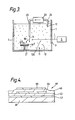
- FIG. 3 illustrates a modification of the method described above with reference to Figure 1.
- the substrate 10 ⁇ is mounted on a support 2 ⁇ so that the surface 10a ⁇ is horizontal.
- a circulating pump 23 having an inlet pipe 24 and an outlet pipe 25 is mounted to the top of the tank to cause vertical circulation within the suspension 11 so that, as indicated by the arrow A in Figure 3, there is a resultant downward force of particles just to one side of the substrate 10.
- the electromagnetic radiation source 5 when activated provides a beam of electromagnetic radiation L at an angle to the downward force indicated by the arrow A so that particles 12a of the given size interacting resonantly with the beam L are deflected as indicated by the arrow B so as to be deposited onto the substrate 10.
- an electromagnetic radiation source 5 with several different wavelengths, for example a tuneable continuous wave or pulsed laser, particles of several different sizes may be separated and deposited.
- the use of a method embodying the invention enables a quantum dot structure to be formed simply and easily without the need for the use of electron beam lithography or ion etching. Moreover, because most of the applications of quantum dot structures are optical, the selection of the particles to form the quantum dot structure by using the above descibed optical resonance ensures that only optically active particles of the correct size are used.
- Figure 4 illustrates very schematically, and in cross-section, one example of an opto-electronic device incorporating a quantum well structure manufactured using a method in accordance with the invention.
- the device 40 comprises a substrate 41, for example a glass substrate, onto which a transparent electrically conductive layer 42, for example a layer of indium tin oxide, is provided.
- the electrically conductive layer 42 is covered with a layer 43 of an insulating material, which may be a cured layer of the carrier material mentioned above, for example a layer of PMMA, polyimide or an acrylic resin.
- the active area 44 which is manufactured as described above and this consists of one or more layers of the carrier material into which particles of a selected semiconductor material have been embedded using one of the methods described above.
- a further layer 45 of the insulating material covers the active area and an electrically conductive contact layer 46, for example an aluminium contact layer is provided on top of the further layer 45.
- an electrically conductive contact layer 46 for example an aluminium contact layer is provided on top of the further layer 45.
- Figure 5 is a schematic perspective view of an optical switching device in which the active area is a quantum dot structure formed using a method in accordance with the invention.
- the device 50 comprises substrate 51, for example a glass substrate.
- a layer of the carrier material for example PMMA, polyimide or an acrylic resin, is spun-coated onto the substrate 51 and a quantum dot structure manufactured using one of the methods described above. Using conventional photolithographic and etching techniques the quantum dot structure is patterned to define a strip 52.
- a cladding layer is provided over the strip 52.
- a window is then opened in the cladding layer to expose the surface of an area 521 of the strip 52 and a further layer of the carrier material is then spun-coated onto the cladding layer and photolithographically patterned to define a strip 53 which contacts the strip 52 at the area 52 adjacent one end 53a of the strip 53.
- a final cladding layer (not shown) is provided over the strip 53.
- the cladding layers are selected so as to have a refractive index lower than that of the carrier material so that the strips 52 and 53 form waveguides.
- the substrate 51 is made of a light glass such as a lithium glass then the strip 52 may be formed directly onto the substrate.
- a low refractive index cladding layer 51a may be provided, as indicated by the dashed line, between the substrate 51 and the strip 52.
- the cladding layers may be, in this example, formed of a material such as lithium glass or of, for example, collodian.
- Electromagnetic radiation having a wavelength just above the confined exciton resonance of the quantum dot structure is introduced into one end 52a of the strip 52 by an optical fibre coupling 54 as is known in the art.
- the quantum dot structure containing strip 52 will have a higher refractive index than the strip 53 and accordingly the area 53 of the strip 53 in contact with the area 52 of the strip 52 will act as a waveguide cladding layer causing light travelling along the strip 52 to be output at the other end 52b of the strip 52 as indicated by the arrow A in Figure 5.
- the quantum dot structure containing strip 52 acts as a non-linear medium and has a refractive index which varies with the intensity of the electromagnetic radiation travelling along the strip 52.
- the intensity of the electromagnetic radiation reaches a given level, the refractive index of the strip 52 is so reduced that the electromagnetic radiation can leak out of the strip 52 into the strip 53 providing an output from the other end 53b of the of the strip 53 as indicated by the arrow B.
- a bistable optical switch is formed in which the intensity of the incident electromagnetic radiation determines whether an output is provided from the end 53b of the strip 53 or the end 52b of the strip 52.
- Various other geometries for similar bistable optical switches are, of course, possible.
- a quantum dot structure produced using a method in accordance with the invention may be used directly in an optical device such as a light emitting device or an optical switching device, it may be possible where the carrier material can be dissolved without affecting the particles or quantum dots to collect the particles deposited onto the substrate and then redisperse them as a suspension in an appropriate medium and then repeat the method described above with reference to Figure 1, 2 or 3 so as to provide a quantum dot structure in which the size of the particles is even more closely confined to a particular desired size.
- the carrier medium can be manipulated, for example by extrusion, it may be possible to remove a layer of carrier material in which a quantum dot structure has been formed from any underlying substrate and then shape the carrier material, for example by extrusion, to provide, for example, optical fibres of the non-linear quantum dot containing material.
Landscapes
- Chemical & Material Sciences (AREA)
- Engineering & Computer Science (AREA)
- Physics & Mathematics (AREA)
- Nanotechnology (AREA)
- Crystallography & Structural Chemistry (AREA)
- Nonlinear Science (AREA)
- Materials Engineering (AREA)
- General Physics & Mathematics (AREA)
- Organic Chemistry (AREA)
- Metallurgy (AREA)
- Optics & Photonics (AREA)
- Mathematical Physics (AREA)
- Theoretical Computer Science (AREA)
- Biophysics (AREA)
- Life Sciences & Earth Sciences (AREA)
- Composite Materials (AREA)
- Condensed Matter Physics & Semiconductors (AREA)
- Dispersion Chemistry (AREA)
- Semiconductor Lasers (AREA)
- Physical Deposition Of Substances That Are Components Of Semiconductor Devices (AREA)
- Recrystallisation Techniques (AREA)
- Crystals, And After-Treatments Of Crystals (AREA)
Applications Claiming Priority (2)
| Application Number | Priority Date | Filing Date | Title |
|---|---|---|---|
| GB8803295A GB2215122A (en) | 1988-02-12 | 1988-02-12 | A method of forming a quantum dot structure |
| GB8803295 | 1988-02-12 |
Publications (2)
| Publication Number | Publication Date |
|---|---|
| EP0328202A2 true EP0328202A2 (de) | 1989-08-16 |
| EP0328202A3 EP0328202A3 (de) | 1991-03-27 |
Family
ID=10631616
Family Applications (1)
| Application Number | Title | Priority Date | Filing Date |
|---|---|---|---|
| EP19890200251 Pending EP0328202A3 (de) | 1988-02-12 | 1989-02-06 | Verfahren zur Herstellung einer Quanteninselnstruktur |
Country Status (4)
| Country | Link |
|---|---|
| EP (1) | EP0328202A3 (de) |
| JP (1) | JPH01244611A (de) |
| KR (1) | KR890013720A (de) |
| GB (1) | GB2215122A (de) |
Cited By (13)
| Publication number | Priority date | Publication date | Assignee | Title |
|---|---|---|---|---|
| WO1996010282A1 (en) * | 1994-09-29 | 1996-04-04 | British Telecommunications Public Limited Company | Optical fibre with quantum dots |
| WO1997004906A1 (en) * | 1995-07-27 | 1997-02-13 | Isis Innovation Limited | Method of producing metal quantum dots |
| US6692031B2 (en) | 1998-12-31 | 2004-02-17 | Mcgrew Stephen P. | Quantum dot security device and method |
| WO2006003584A3 (en) * | 2004-06-28 | 2006-03-23 | Koninkl Philips Electronics Nv | Field-effect transistors fabricated by wet chemical deposition |
| US8128249B2 (en) | 2007-08-28 | 2012-03-06 | Qd Vision, Inc. | Apparatus for selectively backlighting a material |
| US8405063B2 (en) | 2007-07-23 | 2013-03-26 | Qd Vision, Inc. | Quantum dot light enhancement substrate and lighting device including same |
| US8642977B2 (en) | 2006-03-07 | 2014-02-04 | Qd Vision, Inc. | Article including semiconductor nanocrystals |
| US8718437B2 (en) | 2006-03-07 | 2014-05-06 | Qd Vision, Inc. | Compositions, optical component, system including an optical component, devices, and other products |
| US8836212B2 (en) | 2007-01-11 | 2014-09-16 | Qd Vision, Inc. | Light emissive printed article printed with quantum dot ink |
| US9874674B2 (en) | 2006-03-07 | 2018-01-23 | Samsung Electronics Co., Ltd. | Compositions, optical component, system including an optical component, devices, and other products |
| US9929325B2 (en) | 2012-06-05 | 2018-03-27 | Samsung Electronics Co., Ltd. | Lighting device including quantum dots |
| US9945991B2 (en) | 2013-09-16 | 2018-04-17 | Lg Chem, Ltd. | Light-scattering sheet, electronic device comprising same, and method for producing same |
| US9951438B2 (en) | 2006-03-07 | 2018-04-24 | Samsung Electronics Co., Ltd. | Compositions, optical component, system including an optical component, devices, and other products |
Families Citing this family (6)
| Publication number | Priority date | Publication date | Assignee | Title |
|---|---|---|---|---|
| GB2241348A (en) * | 1990-02-20 | 1991-08-28 | British Telecomm | Optical modulator |
| GB9125727D0 (en) * | 1991-12-03 | 1992-01-29 | Hitachi Europ Ltd | Non-linear optical device |
| ES2299408B1 (es) * | 2007-10-18 | 2009-06-12 | Thyssenkrupp Elevator (Es/Pbb) Ltd. | Sistema de guiado autoportante para pasillos rodantes. |
| US11231180B2 (en) | 2017-02-17 | 2022-01-25 | Lg Electronics Inc. | Knob assembly for cook top |
| US10935249B2 (en) | 2017-02-17 | 2021-03-02 | Lg Electronics Inc. | Knob assembly for cook top |
| EP3591495B1 (de) | 2017-02-17 | 2021-09-29 | Lg Electronics Inc. | Gargerät |
Family Cites Families (6)
| Publication number | Priority date | Publication date | Assignee | Title |
|---|---|---|---|---|
| US4340617A (en) * | 1980-05-19 | 1982-07-20 | Massachusetts Institute Of Technology | Method and apparatus for depositing a material on a surface |
| US4327288A (en) * | 1980-09-29 | 1982-04-27 | Bell Telephone Laboratories, Incorporated | Method for focusing neutral atoms, molecules and ions |
| US4359485A (en) * | 1981-05-01 | 1982-11-16 | Bell Telephone Laboratories, Incorporated | Radiation induced deposition of metal on semiconductor surfaces |
| US4625071A (en) * | 1984-11-05 | 1986-11-25 | Chronar Corp. | Particulate semiconductors and devices |
| JPS61117271A (ja) * | 1984-11-13 | 1986-06-04 | Agency Of Ind Science & Technol | レ−ザ蒸着法 |
| JPS623095A (ja) * | 1985-06-07 | 1987-01-09 | モリソン・パンプス・エスエイ・(プロプライアタリ−)・リミテツド | 結晶生長法 |
-
1988
- 1988-02-12 GB GB8803295A patent/GB2215122A/en not_active Withdrawn
-
1989
- 1989-02-06 EP EP19890200251 patent/EP0328202A3/de active Pending
- 1989-02-09 KR KR1019890001439A patent/KR890013720A/ko not_active Withdrawn
- 1989-02-10 JP JP1030050A patent/JPH01244611A/ja active Pending
Cited By (20)
| Publication number | Priority date | Publication date | Assignee | Title |
|---|---|---|---|---|
| US5881200A (en) * | 1994-09-29 | 1999-03-09 | British Telecommunications Public Limited Company | Optical fibre with quantum dots |
| WO1996010282A1 (en) * | 1994-09-29 | 1996-04-04 | British Telecommunications Public Limited Company | Optical fibre with quantum dots |
| WO1997004906A1 (en) * | 1995-07-27 | 1997-02-13 | Isis Innovation Limited | Method of producing metal quantum dots |
| US5965212A (en) * | 1995-07-27 | 1999-10-12 | Isis Innovation Limited | Method of producing metal quantum dots |
| US6692031B2 (en) | 1998-12-31 | 2004-02-17 | Mcgrew Stephen P. | Quantum dot security device and method |
| WO2006003584A3 (en) * | 2004-06-28 | 2006-03-23 | Koninkl Philips Electronics Nv | Field-effect transistors fabricated by wet chemical deposition |
| US9874674B2 (en) | 2006-03-07 | 2018-01-23 | Samsung Electronics Co., Ltd. | Compositions, optical component, system including an optical component, devices, and other products |
| US10393940B2 (en) | 2006-03-07 | 2019-08-27 | Samsung Electronics Co., Ltd. | Compositions, optical component, system including an optical component, devices, and other products |
| US9951438B2 (en) | 2006-03-07 | 2018-04-24 | Samsung Electronics Co., Ltd. | Compositions, optical component, system including an optical component, devices, and other products |
| US8642977B2 (en) | 2006-03-07 | 2014-02-04 | Qd Vision, Inc. | Article including semiconductor nanocrystals |
| US8718437B2 (en) | 2006-03-07 | 2014-05-06 | Qd Vision, Inc. | Compositions, optical component, system including an optical component, devices, and other products |
| US8836212B2 (en) | 2007-01-11 | 2014-09-16 | Qd Vision, Inc. | Light emissive printed article printed with quantum dot ink |
| US8759850B2 (en) | 2007-07-23 | 2014-06-24 | Qd Vision, Inc. | Quantum dot light enhancement substrate |
| US9680054B2 (en) | 2007-07-23 | 2017-06-13 | Samsung Electronics Co., Ltd. | Quantum dot light enhancement substrate and lighting device including same |
| US9276168B2 (en) | 2007-07-23 | 2016-03-01 | Qd Vision, Inc. | Quantum dot light enhancement substrate and lighting device including same |
| US8405063B2 (en) | 2007-07-23 | 2013-03-26 | Qd Vision, Inc. | Quantum dot light enhancement substrate and lighting device including same |
| US10096744B2 (en) | 2007-07-23 | 2018-10-09 | Samsung Electronics Co., Ltd. | Quantum dot light enhancement substrate and lighting device including same |
| US8128249B2 (en) | 2007-08-28 | 2012-03-06 | Qd Vision, Inc. | Apparatus for selectively backlighting a material |
| US9929325B2 (en) | 2012-06-05 | 2018-03-27 | Samsung Electronics Co., Ltd. | Lighting device including quantum dots |
| US9945991B2 (en) | 2013-09-16 | 2018-04-17 | Lg Chem, Ltd. | Light-scattering sheet, electronic device comprising same, and method for producing same |
Also Published As
| Publication number | Publication date |
|---|---|
| JPH01244611A (ja) | 1989-09-29 |
| GB2215122A (en) | 1989-09-13 |
| GB8803295D0 (en) | 1988-03-09 |
| KR890013720A (ko) | 1989-09-25 |
| EP0328202A3 (de) | 1991-03-27 |
Similar Documents
| Publication | Publication Date | Title |
|---|---|---|
| EP0328202A2 (de) | Verfahren zur Herstellung einer Quanteninselnstruktur | |
| US7402832B2 (en) | Quantum dots of group IV semiconductor materials | |
| US20040126072A1 (en) | Optical devices with engineered nonlinear nanocomposite materials | |
| US8357980B2 (en) | Plasmonic high-speed devices for enhancing the performance of microelectronic devices | |
| US9008467B2 (en) | Nanoparticle-based quantum confined stark effect modulator | |
| CA1204369A (en) | Method for manufacturing optical waveguides in semiconductors | |
| EP0606776A2 (de) | Emission und Detektion von Terahertz-Strahlung | |
| CA1284835C (en) | All-optical modulator with a channel waveguide | |
| US5004325A (en) | Optical processing using a multilayer heterostructure | |
| EP2422414B1 (de) | Passive terahertz-strahlungsquelle | |
| US7546017B2 (en) | Electro-photonic modulators | |
| US20060279829A1 (en) | Electro-absorption modulator device and methods for fabricating the same | |
| EP0131042B1 (de) | Die intensität eines lichtstrahls gerichtet auf eine integrierte schaltung steuert den strahl | |
| US20110101211A1 (en) | Device for trapping particles | |
| US5637883A (en) | Optically addressed spatial light modulator using an intrinsic semiconductor active material and high resistivity cladding layers | |
| Huang et al. | Depletion edge translation waveguide crossing optical switch | |
| Mentzer | Principles of optical circuit engineering | |
| CN114488578B (zh) | 一种基于声子极化激元的相位调制方法 | |
| US20050084195A1 (en) | Method and apparatus for forming lateral electrical contacts for photonic crystal devices | |
| WO1989007832A1 (en) | Semiconductor superlattice heterostructures fabrication methods, structures and devices | |
| JP2026009075A (ja) | 光スイッチング素子及び光スイッチング素子の製造方法 | |
| Charbonneau et al. | Photonic integrated circuits fabricated using quantum well intermixing | |
| Yamamoto et al. | Photonic crystal preparation by a wafer bonding approach | |
| Colak | Devices and applications of II-VI compounds | |
| Bhattacharya et al. | GaAs/AlxOy photonic bandgap material fabrication and characterization |
Legal Events
| Date | Code | Title | Description |
|---|---|---|---|
| PUAI | Public reference made under article 153(3) epc to a published international application that has entered the european phase |
Free format text: ORIGINAL CODE: 0009012 |
|
| AK | Designated contracting states |
Kind code of ref document: A2 Designated state(s): DE FR GB NL |
|
| PUAL | Search report despatched |
Free format text: ORIGINAL CODE: 0009013 |
|
| 18W | Application withdrawn |
Withdrawal date: 19910111 |
|
| AK | Designated contracting states |
Kind code of ref document: A3 Designated state(s): DE FR GB NL |
|
| D18W | Application withdrawn (deleted) | ||
| STAA | Information on the status of an ep patent application or granted ep patent |
Free format text: STATUS: THE APPLICATION IS DEEMED TO BE WITHDRAWN |
|
| 18D | Application deemed to be withdrawn |
Effective date: 19910829 |
|
| D18W | Application withdrawn (deleted) |