EP0328941A1 - Procédé et dispositif de commutation du courant entre des valves déconnectables dans un redresseur de courant - Google Patents
Procédé et dispositif de commutation du courant entre des valves déconnectables dans un redresseur de courant Download PDFInfo
- Publication number
- EP0328941A1 EP0328941A1 EP89101739A EP89101739A EP0328941A1 EP 0328941 A1 EP0328941 A1 EP 0328941A1 EP 89101739 A EP89101739 A EP 89101739A EP 89101739 A EP89101739 A EP 89101739A EP 0328941 A1 EP0328941 A1 EP 0328941A1
- Authority
- EP
- European Patent Office
- Prior art keywords
- valve
- current
- branch
- signal
- switch
- Prior art date
- Legal status (The legal status is an assumption and is not a legal conclusion. Google has not performed a legal analysis and makes no representation as to the accuracy of the status listed.)
- Ceased
Links
- 238000000034 method Methods 0.000 title claims description 9
- 238000001514 detection method Methods 0.000 claims description 13
- 230000000903 blocking effect Effects 0.000 claims description 11
- 230000003111 delayed effect Effects 0.000 claims description 5
- 101100449816 Saccharomyces cerevisiae (strain ATCC 204508 / S288c) GTO1 gene Proteins 0.000 claims description 3
- 101100449819 Saccharomyces cerevisiae (strain ATCC 204508 / S288c) GTO3 gene Proteins 0.000 claims description 2
- 238000007599 discharging Methods 0.000 claims description 2
- 238000002955 isolation Methods 0.000 claims description 2
- 230000001960 triggered effect Effects 0.000 claims description 2
- 239000004065 semiconductor Substances 0.000 description 4
- 230000001419 dependent effect Effects 0.000 description 2
- 230000003321 amplification Effects 0.000 description 1
- 239000003990 capacitor Substances 0.000 description 1
- 230000015556 catabolic process Effects 0.000 description 1
- 230000007423 decrease Effects 0.000 description 1
- 238000011161 development Methods 0.000 description 1
- 230000018109 developmental process Effects 0.000 description 1
- 238000003199 nucleic acid amplification method Methods 0.000 description 1
- 239000013307 optical fiber Substances 0.000 description 1
- 230000003071 parasitic effect Effects 0.000 description 1
- 238000000926 separation method Methods 0.000 description 1
- 238000007493 shaping process Methods 0.000 description 1
- 238000011144 upstream manufacturing Methods 0.000 description 1
Images
Classifications
-
- H—ELECTRICITY
- H02—GENERATION; CONVERSION OR DISTRIBUTION OF ELECTRIC POWER
- H02M—APPARATUS FOR CONVERSION BETWEEN AC AND AC, BETWEEN AC AND DC, OR BETWEEN DC AND DC, AND FOR USE WITH MAINS OR SIMILAR POWER SUPPLY SYSTEMS; CONVERSION OF DC OR AC INPUT POWER INTO SURGE OUTPUT POWER; CONTROL OR REGULATION THEREOF
- H02M7/00—Conversion of AC power input into DC power output; Conversion of DC power input into AC power output
- H02M7/42—Conversion of DC power input into AC power output without possibility of reversal
- H02M7/44—Conversion of DC power input into AC power output without possibility of reversal by static converters
- H02M7/48—Conversion of DC power input into AC power output without possibility of reversal by static converters using discharge tubes with control electrode or semiconductor devices with control electrode
- H02M7/505—Conversion of DC power input into AC power output without possibility of reversal by static converters using discharge tubes with control electrode or semiconductor devices with control electrode using devices of a thyratron or thyristor type requiring extinguishing means
- H02M7/515—Conversion of DC power input into AC power output without possibility of reversal by static converters using discharge tubes with control electrode or semiconductor devices with control electrode using devices of a thyratron or thyristor type requiring extinguishing means using semiconductor devices only
- H02M7/521—Conversion of DC power input into AC power output without possibility of reversal by static converters using discharge tubes with control electrode or semiconductor devices with control electrode using devices of a thyratron or thyristor type requiring extinguishing means using semiconductor devices only in a bridge configuration
Definitions
- the invention relates to a method for commutating an impressed current between valve branches of a converter device, the valve branches of which each have a semiconductor valve device with a valve circuit which can be switched off and can be blocked in the reverse direction.
- the forward direction of such a valve branch is given by its arrangement in the converter device such that a current flow should only be possible in this direction.
- valve branch In the opposite direction (“backward direction”) the valve branch is to block, which is inherently the case with a symmetrically blocking GTO (ie a GTO which is blocking when actuated with a switch-off signal regardless of the polarity of the anode / cathode voltage) and in the case of a transistor or an asymmetrically blocking GTO (ie a GTO which can switch off a current when the anode / cathode voltage is positive, but has no blocking capacity when the voltage polarity is reversed), the series connection can be achieved with a diode. For commutating the current the valve device of the downstream valve branch is switched off and the valve device of the receiving valve branch is switched on.
- GTO symmetrically blocking GTO
- a GTO which can switch off a current when the anode / cathode voltage is positive, but has no blocking capacity when the voltage polarity is reversed
- bridge circuits are operated with valve branches of this type that can be switched off and can be blocked in the reverse direction in the area of natural commutation, then it is sufficient to switch on the receiving valve branch, whereby the emitting semiconductor valve branch is acted upon by negative anode / cathode voltage and goes out.
- a backflow initially forms, which then breaks off with a steep flank. However, this creates an overvoltage that is caused by the para dependent inductance of the circuit is dependent and can assume such high values that the valve is at risk.
- valve circuit known from conventional thyristor circuits which has a particularly low impedance and low inductance, can be used, but this then loads the valve with a steep current surge when it is switched on.
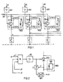
- FIG. 1 shows a preferred embodiment of a half of a bridge circuit which is impressed with a predetermined, practically constant direct current via the inductor DR and which e.g. contains three bridge branches, each with a valve device, this valve device consisting of the transistors T1, T3, T5 with the series diodes D1, D3, D5.
- Control circuits AS1, AS3, AS5 each form the control voltages for the control connections of the valves from corresponding control signals s1, s3, s5 by amplification and pulse shaping.
- An RCD network is connected in parallel to the transistor-diode series circuit, but this network has, in some cases, considerable parasitic inductances, as indicated in FIG. 1.
- Control circuit and RCD protection circuit are commercially available and e.g. known from Appendix 2 to "Thyristor Applications Notes ⁇ AN-315 (USA, 1982) from the company" International Rectifier ".
- valve T1 As long as the valve T1 carries current when the valves T3 and T5 are blocked, the voltage of the direct voltage connection P is up to the breakdown voltage of the valve branch at the three-phase connection R of the bridge circuit. If, with the polarity of the three-phase connections shown, corresponding valve signals s1 and s3 are switched on and valve branch T3 is switched on at the same time, valve T1 is blocked, valve T3 takes over the current, but valve T1 causes a reverse current and a polarity reversal of the voltages in the Valve circuit. Tears this reverse current decreases, the leakage inductances generate a high peak of the now negative anode / cathode voltage of the Venil T1, which is endangered thereby.
- the object of the invention is to avoid this risk by intervening in the circuit or the control of the valves as simply as possible.
- the invention is based on the knowledge that in the current-giving semiconductor valve branch the reverse current and the associated dangerous reverse voltage only occur when the current-giving valve branch changes into the blocking state when the valve voltage is negative.
- This negative valve voltage always arises when the current-absorbing valve was initially blocked with a positive anode voltage and is switched on to take over the current as long as the releasing valve is still conducting. The backflow does not occur, however, if the current-giving valve is switched off via its control voltage in such a way that a positive anode voltage first appears at this valve. If the current-absorbing valve is subsequently ignited, ie only after the current through the current-giving valve has been significantly reduced, then a negative anode voltage which occurs at the now blocked current-giving valve can no longer cause any significant danger.
- the switching on of the valve device in the receiving branch is delayed until the valve is practically de-energized by switching off the valve device in the discharging branch. During this delay time, both valves are blocked, the current can commutate to the valve circuit in the output branch and generate the desired positive anode voltage at the switched-off valve.
- the end of the delay time is determined by the fact that a current path must be opened for the direct current supplied by the direct current circuit via the receiving branch, so that there are no overvoltages on the valve devices.
- a current path must be opened for the direct current supplied by the direct current circuit via the receiving branch, so that there are no overvoltages on the valve devices.
- a current monitor e.g. can be ensured by a current monitor, a voltage monitor or a time monitor, so there is a pause between switching off one valve and switching on the other valve, which is inherently inadmissible in conventional converters with impressed direct current, but a considerable time according to the invention can last.
- a state detection device Z detects the currentlessness of the switched-off valve and generates a corresponding state signal zl.
- a release device FG is connected upstream of the control input of the valve or its control device AS, which only releases the switch-on signal of a valve device to be switched on when the status detection of the valve device to be switched off emits the status signal which detects the currentlessness.
- the state detection device Z of the GTO can be connected to its connections, in particular to a current detector arranged in the valve feed lines.
- the release signal for other valve branches is therefore only generated when the detected current through the valve falls below a threshold value.
- a separate current detector is connected to each valve branch of the converter device.
- the voltage at the valve device of the current branch can also be detected via a corresponding voltage detector in order to delay its switching on via the corresponding status signal z1 and the release device FG of the valve branch to be switched on until the detected voltage exceeds a threshold value.
- This threshold value must be matched to the maximum blocking voltage present in the blocked state, and should therefore be chosen to be relatively high, so that the safety distance from the interference voltage to be suppressed can only be small.
- the state detection device Z is connected to the control connection of the GTO in order to detect its control voltage and to only generate the release signal when this detected control voltage reaches a predetermined threshold value.
- any potential separation required between the condition detection device Z of one valve and the release device FG of other valves can be done optically via optocouplers OP or optical fibers with photodiodes, or also magnetically.
- the release device blocks the switch-on signal s1 of the GTO until the corresponding status signals z3, z5 of the other valves of the same bridge half (or the other valves of the converter device which are capable and intended to deliver the current to be taken over by the GTO) report that these valves are currentless .
- This is done by a logic operation, which in the simplest case that the switch-on state of the control signal s1 and the released state of the signals z3 and z5 are each indicated by "1”, can be a simple AND gate.
- This simple variant has the advantage that no electrical isolation is required.
- the optimal time delay depends on many operating parameters, e.g. Temperature and current as well as the storage time of the GTO or the runtimes in the signal processing. It can therefore be advantageous to change the storage time of the delay element T as a function of operating parameters of the converter device.
- the invention can be applied to very different converter devices, for example bridges with different phase numbers or pulse numbers, bridges connected in parallel or semi-controlled bridges.
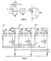
- 4 shows this using the example of a semi-controlled bridge.
- the controlled commutation of the current takes place only in one bridge half, so that only the valve devices of this controlled bridge half are each to be equipped with a release device FG 1, FG 3, FG 5 and a corresponding status detection Z1, Z3, Z5.
- the status signal for the de-energized status of a valve is in each case applied to the inputs of the release devices on the other valve devices.
- other semiconductor valves can also be used here instead of the symmetrically blocking cut-off thyristors GTO1, GTO3, GTO5.
- the valve connection required in each case is not shown in FIG. 4.
- the converter devices equipped with it can be operated on the network or on machines.
Landscapes
- Engineering & Computer Science (AREA)
- Power Engineering (AREA)
- Power Conversion In General (AREA)
- Rectifiers (AREA)
- Inverter Devices (AREA)
Applications Claiming Priority (2)
| Application Number | Priority Date | Filing Date | Title |
|---|---|---|---|
| DE3804808 | 1988-02-16 | ||
| DE3804808 | 1988-02-16 |
Publications (1)
| Publication Number | Publication Date |
|---|---|
| EP0328941A1 true EP0328941A1 (fr) | 1989-08-23 |
Family
ID=6347521
Family Applications (1)
| Application Number | Title | Priority Date | Filing Date |
|---|---|---|---|
| EP89101739A Ceased EP0328941A1 (fr) | 1988-02-16 | 1989-02-01 | Procédé et dispositif de commutation du courant entre des valves déconnectables dans un redresseur de courant |
Country Status (3)
| Country | Link |
|---|---|
| US (1) | US4920473A (fr) |
| EP (1) | EP0328941A1 (fr) |
| JP (1) | JPH01248956A (fr) |
Cited By (1)
| Publication number | Priority date | Publication date | Assignee | Title |
|---|---|---|---|---|
| WO2005011096A1 (fr) | 2003-07-24 | 2005-02-03 | The Kansai Electric Power Co., Inc. | Appareil convertisseur continu-alternatif |
Families Citing this family (2)
| Publication number | Priority date | Publication date | Assignee | Title |
|---|---|---|---|---|
| DE3934044A1 (de) * | 1989-09-08 | 1991-03-21 | Asea Brown Boveri | Verfahren und vorrichtung zur bildung eines loeschsperrsignals fuer abschaltbare leistungshalbleiter |
| US9752990B2 (en) | 2013-09-30 | 2017-09-05 | Honeywell International Inc. | Low-powered system for driving a fuel control mechanism |
Citations (4)
| Publication number | Priority date | Publication date | Assignee | Title |
|---|---|---|---|---|
| US4342076A (en) * | 1981-02-12 | 1982-07-27 | Westinghouse Electric Corp. | Transistor turn off current sensing circuit |
| US4342976A (en) * | 1980-02-01 | 1982-08-03 | Hasler Ag | Pulse transformer |
| GB2137029A (en) * | 1983-03-14 | 1984-09-26 | Westinghouse Electric Corp | Switching Control Circuit for DC/AC Inverter |
| US4597038A (en) * | 1984-07-26 | 1986-06-24 | Westinghouse Electric Corp. | Switching overlap protection by control gate impedance monitoring |
Family Cites Families (4)
| Publication number | Priority date | Publication date | Assignee | Title |
|---|---|---|---|---|
| DE3434607A1 (de) * | 1984-09-18 | 1986-03-27 | Siemens AG, 1000 Berlin und 8000 München | Verfahren und vorrichtung zum betreiben eines abschalthyristors |
| DE3537050A1 (de) * | 1985-06-19 | 1987-01-02 | Siemens Ag | Verfahren und vorrichtung zur erkennung des sperrzustandes eines abschaltbaren thyristors |
| US4641231A (en) * | 1985-12-06 | 1987-02-03 | General Electric Company | Apparatus and method for failure testing of a control turn-off semiconductor |
| US4775925A (en) * | 1987-11-23 | 1988-10-04 | General Electric Company | Method and apparatus for determining the control electrode to cathode junction voltage of a control turn-off semiconductor device and use of such determined voltage in the control of the device |
-
1989
- 1989-02-01 EP EP89101739A patent/EP0328941A1/fr not_active Ceased
- 1989-02-14 US US07/310,728 patent/US4920473A/en not_active Expired - Fee Related
- 1989-02-14 JP JP1034878A patent/JPH01248956A/ja active Pending
Patent Citations (4)
| Publication number | Priority date | Publication date | Assignee | Title |
|---|---|---|---|---|
| US4342976A (en) * | 1980-02-01 | 1982-08-03 | Hasler Ag | Pulse transformer |
| US4342076A (en) * | 1981-02-12 | 1982-07-27 | Westinghouse Electric Corp. | Transistor turn off current sensing circuit |
| GB2137029A (en) * | 1983-03-14 | 1984-09-26 | Westinghouse Electric Corp | Switching Control Circuit for DC/AC Inverter |
| US4597038A (en) * | 1984-07-26 | 1986-06-24 | Westinghouse Electric Corp. | Switching overlap protection by control gate impedance monitoring |
Cited By (3)
| Publication number | Priority date | Publication date | Assignee | Title |
|---|---|---|---|---|
| WO2005011096A1 (fr) | 2003-07-24 | 2005-02-03 | The Kansai Electric Power Co., Inc. | Appareil convertisseur continu-alternatif |
| EP1653598A4 (fr) * | 2003-07-24 | 2009-06-03 | Kansai Electric Power Co | Appareil convertisseur continu-alternatif |
| US7570502B2 (en) | 2003-07-24 | 2009-08-04 | The Kansai Electric Power Co., Inc. | Inverter apparatus comprising switching elements |
Also Published As
| Publication number | Publication date |
|---|---|
| US4920473A (en) | 1990-04-24 |
| JPH01248956A (ja) | 1989-10-04 |
Similar Documents
| Publication | Publication Date | Title |
|---|---|---|
| DE112013001123B4 (de) | Leistungsschaltung | |
| EP0321865B1 (fr) | Onduleur troix niveaux à déchargement de commutation et à perte réduite | |
| DE102016224706B4 (de) | Gate-Antriebsschaltung für Halbleiterschaltgeräte | |
| DE112016000220B4 (de) | Leistungswandlungsausrüstung | |
| EP3853957B1 (fr) | Commutateur électronique à protection contre les surtensions | |
| DE3640546C2 (fr) | ||
| DE112011103585T5 (de) | Stromumformervorrichtung | |
| WO2022243196A1 (fr) | Procédé de fonctionnement d'un système d'alimentation protégé contre les courts-circuits et système d'alimentation protégé contre les courts-circuits | |
| DE3246706A1 (de) | Stromversorgungsvorrichtung fuer einen wechselstromverbraucher | |
| EP3403270A1 (fr) | Commutateur pour courant continu | |
| DE102013226795A1 (de) | Schaltungsanordnung für einen Notlauf eines mehrphasigen Spannungswandlers mittels speziellen Betriebsverfahren | |
| DE3405793A1 (de) | Verfahren und vorrichtung zum kurzschlussschutz eines stromrichtergeraetes mit gto-thyristoren | |
| DE3905645A1 (de) | Ansteuerverfahren zur verbesserung des ueberstromabschaltverhaltens von leistungshalbleiterschaltern mit mos-steuereingang | |
| DE3743437C1 (en) | Low-loss, three-point invertor which is relieved of switching loads | |
| DE10031778A1 (de) | Verfahren und Vorrichtung zur Regelung der Stromanstiegsgeschwindigkeit | |
| DE2214949A1 (de) | Steuereinrichtung fur ein Steuer bares Bauelement | |
| DE19920625A1 (de) | Schutzschaltung für einen Schalter sowie Schaltnetzteil | |
| DE102015206031B4 (de) | Vorrichtung zum Begrenzen einer über einem Leistungsschalter abfallenden Spannung, Spannungszwischenkreisumrichter sowie Verfahren | |
| WO2018108725A1 (fr) | Agencement de commutation et procédé d'alimentation en courant et de déchargement d'une bobine | |
| DE4031505C2 (de) | Gleichspannungs-Stromversorgung mit Einschaltstrombegrenzung | |
| DE2716367A1 (de) | Schutzbeschaltung fuer einen transistor | |
| AT523936A4 (de) | Verfahren und vorrichtung zum steuern eines halbleiterschalters | |
| EP3994792A1 (fr) | Procédé de précharge de modules d'un convertisseur multiniveau modulaire | |
| EP0177779B1 (fr) | Montage avec un circuit d'alimentation pour alimenter une résistance de charge | |
| DE3815471C2 (de) | Verlustarme Beschaltung an mindestens einem abschaltbaren Ventil |
Legal Events
| Date | Code | Title | Description |
|---|---|---|---|
| PUAI | Public reference made under article 153(3) epc to a published international application that has entered the european phase |
Free format text: ORIGINAL CODE: 0009012 |
|
| AK | Designated contracting states |
Kind code of ref document: A1 Designated state(s): CH DE FR GB IT LI SE |
|
| 17P | Request for examination filed |
Effective date: 19890905 |
|
| 17Q | First examination report despatched |
Effective date: 19910719 |
|
| STAA | Information on the status of an ep patent application or granted ep patent |
Free format text: STATUS: THE APPLICATION HAS BEEN REFUSED |
|
| 18R | Application refused |
Effective date: 19920124 |