EP0329447B1 - Vorrichtung für die Determination der Temperatur von Wafern oder Dünnschichten - Google Patents
Vorrichtung für die Determination der Temperatur von Wafern oder Dünnschichten Download PDFInfo
- Publication number
- EP0329447B1 EP0329447B1 EP89301517A EP89301517A EP0329447B1 EP 0329447 B1 EP0329447 B1 EP 0329447B1 EP 89301517 A EP89301517 A EP 89301517A EP 89301517 A EP89301517 A EP 89301517A EP 0329447 B1 EP0329447 B1 EP 0329447B1
- Authority
- EP
- European Patent Office
- Prior art keywords
- temperature
- energy
- optical
- workpiece
- bandgap
- Prior art date
- Legal status (The legal status is an assumption and is not a legal conclusion. Google has not performed a legal analysis and makes no representation as to the accuracy of the status listed.)
- Expired - Lifetime
Links
- 235000012431 wafers Nutrition 0.000 title description 27
- 230000003287 optical effect Effects 0.000 claims description 82
- 230000003595 spectral effect Effects 0.000 claims description 40
- 238000001514 detection method Methods 0.000 claims description 37
- 230000005540 biological transmission Effects 0.000 claims description 36
- 239000000463 material Substances 0.000 claims description 30
- 229910001218 Gallium arsenide Inorganic materials 0.000 claims description 28
- 238000010438 heat treatment Methods 0.000 claims description 14
- 239000011521 glass Substances 0.000 claims description 9
- 238000012545 processing Methods 0.000 claims description 6
- 239000007787 solid Substances 0.000 claims description 2
- 239000000758 substrate Substances 0.000 claims 2
- 239000004065 semiconductor Substances 0.000 description 36
- 239000000523 sample Substances 0.000 description 27
- 238000000034 method Methods 0.000 description 24
- 238000010521 absorption reaction Methods 0.000 description 23
- 230000006870 function Effects 0.000 description 19
- 238000004140 cleaning Methods 0.000 description 12
- 230000005855 radiation Effects 0.000 description 11
- 230000008569 process Effects 0.000 description 8
- 238000005259 measurement Methods 0.000 description 6
- 238000010606 normalization Methods 0.000 description 5
- 230000004907 flux Effects 0.000 description 4
- 238000012544 monitoring process Methods 0.000 description 4
- 239000003795 chemical substances by application Substances 0.000 description 3
- 150000001875 compounds Chemical class 0.000 description 3
- XUIMIQQOPSSXEZ-UHFFFAOYSA-N Silicon Chemical compound [Si] XUIMIQQOPSSXEZ-UHFFFAOYSA-N 0.000 description 2
- 238000013459 approach Methods 0.000 description 2
- 230000008859 change Effects 0.000 description 2
- 230000007423 decrease Effects 0.000 description 2
- 230000000694 effects Effects 0.000 description 2
- 239000011159 matrix material Substances 0.000 description 2
- 230000007246 mechanism Effects 0.000 description 2
- 238000001451 molecular beam epitaxy Methods 0.000 description 2
- 238000004886 process control Methods 0.000 description 2
- 238000000926 separation method Methods 0.000 description 2
- 229910052710 silicon Inorganic materials 0.000 description 2
- 239000010703 silicon Substances 0.000 description 2
- PMVSDNDAUGGCCE-TYYBGVCCSA-L Ferrous fumarate Chemical compound [Fe+2].[O-]C(=O)\C=C\C([O-])=O PMVSDNDAUGGCCE-TYYBGVCCSA-L 0.000 description 1
- 229910000661 Mercury cadmium telluride Inorganic materials 0.000 description 1
- 238000004616 Pyrometry Methods 0.000 description 1
- BUGBHKTXTAQXES-UHFFFAOYSA-N Selenium Chemical compound [Se] BUGBHKTXTAQXES-UHFFFAOYSA-N 0.000 description 1
- 238000004458 analytical method Methods 0.000 description 1
- 229910052980 cadmium sulfide Inorganic materials 0.000 description 1
- 238000011088 calibration curve Methods 0.000 description 1
- 239000011248 coating agent Substances 0.000 description 1
- 238000000576 coating method Methods 0.000 description 1
- 238000004590 computer program Methods 0.000 description 1
- 238000011109 contamination Methods 0.000 description 1
- 238000001816 cooling Methods 0.000 description 1
- 238000012937 correction Methods 0.000 description 1
- 239000013078 crystal Substances 0.000 description 1
- 238000013500 data storage Methods 0.000 description 1
- 230000001419 dependent effect Effects 0.000 description 1
- 238000011065 in-situ storage Methods 0.000 description 1
- 239000007788 liquid Substances 0.000 description 1
- 230000007935 neutral effect Effects 0.000 description 1
- 239000002245 particle Substances 0.000 description 1
- 239000010453 quartz Substances 0.000 description 1
- 230000011514 reflex Effects 0.000 description 1
- 238000005070 sampling Methods 0.000 description 1
- 229910052711 selenium Inorganic materials 0.000 description 1
- 239000011669 selenium Substances 0.000 description 1
- 230000035945 sensitivity Effects 0.000 description 1
- VYPSYNLAJGMNEJ-UHFFFAOYSA-N silicon dioxide Inorganic materials O=[Si]=O VYPSYNLAJGMNEJ-UHFFFAOYSA-N 0.000 description 1
- 238000001228 spectrum Methods 0.000 description 1
- 239000000725 suspension Substances 0.000 description 1
- 229910052714 tellurium Inorganic materials 0.000 description 1
- PORWMNRCUJJQNO-UHFFFAOYSA-N tellurium atom Chemical compound [Te] PORWMNRCUJJQNO-UHFFFAOYSA-N 0.000 description 1
- 239000010409 thin film Substances 0.000 description 1
- 230000036962 time dependent Effects 0.000 description 1
Images



Classifications
-
- G—PHYSICS
- G01—MEASURING; TESTING
- G01K—MEASURING TEMPERATURE; MEASURING QUANTITY OF HEAT; THERMALLY-SENSITIVE ELEMENTS NOT OTHERWISE PROVIDED FOR
- G01K11/00—Measuring temperature based upon physical or chemical changes not covered by groups G01K3/00, G01K5/00, G01K7/00 or G01K9/00
- G01K11/12—Measuring temperature based upon physical or chemical changes not covered by groups G01K3/00, G01K5/00, G01K7/00 or G01K9/00 using changes in colour, translucency or reflectance
Definitions
- the present invention relates to temperature detection and to process control procedures. More particularly, the invention is applicable to the precise detection as well as control of the temperature of a semiconductor crystal and is especially useful in process steps where contact with the crystalline surface must be avoided.
- An example of an application of the invention involves the processing of GaAs thin layers, or of wafers prior to the growth of epitaxial layers, where the temperature must be accurately known and/or controlled, and no physical contact to the wafer surface can be tolerated.
- a device which has been used in an attempt to overcome these difficulties is the pyrometer, which utilises the black-body (or "gray body") radiation of the sample in order to measure its temperature.
- This method is valid only when the wavelength of the radiation used is such that its characteristic coefficient of absorption is very large in comparison with the reciprocal of the thickness of the wafer or the thin layer.
- Such is rarely the case with wafers or thin layers of semiconductors such as GaAs, since the long wavelength light ( ⁇ > 1000 nanometers) used in pyrometry is hardly absorbed (if at all) by the semiconductor whose bandgap energy exceeds that of the light. Only for thick wafers, having temperatures well above room temperature, can the pyrometric method be applied: in these situations, wavelengths of about 900 nanometers are employed.
- Pyrometers therefore, when used in applications to GaAs or to semiconductors of comparable bandgaps, almost always monitor the temperature of the body on which the semiconductor wafer rests rather than the actual temperature of the semiconductor material.
- the pyrometer (utilising radiation above 900 nanometers) absorbs radiation emitted by the glass faceplate.
- the cathode itself which is totally transparent to such radiation, is not “seen” at all by the pyrometer; and, furthermore, the cathode layer introduces an additional complication by acting as a thin film interference filter. This latter effect causes the pyrometric temperature readings of the glass faceplate itself to be in error - depending on the thickness of the cathode layers. The thinner the cathode layer, the more sensitive the pyrometer reading to small variations in the layers' thickness.
- an optical temperature sensor probe which incorporates a semiconductor body having a bandgap energy which varies as a function of temperature due to the absorption edge of the semiconductor.
- the semiconductor body is arranged to be subjected to radiant energy from a source of radiant energy, the wavelength spectrum of radiant energy output from the body being detected spectroscopically in order to determine the temperature of the semiconductor body.
- the semiconductor body forms a permanent integral part of the temperature sensor probe for measuring the temperatures of external bodies or media and the radiant energy is transmitted to and from the body by optical lightguides (e.g. optical fibres) which are in physical abutting contact with the semiconductor body.
- optical lightguides e.g. optical fibres
- the present invention is based on the monotonic change in the optical absorption coefficient as a function of temperature.
- the controlling phenomenon is the narrowing of the bandgap of the semiconductor [it is the direct optical bandgap in the case of GaAs] with increasing temperature. Since the absorption coefficient for light of a narrow spectral range, whose photon energy is slightly higher than the bandgap energy, depends on the separation between these two energies (i.e. the photon energy and the bandgap energy: see Eq. 2), it follows that the absorption coefficient will depend on the temperature of the GaAs wafer or thin layer.
- the energy of the narrow spectral range employed in this mode must be such that it stays above the band edge at all temperatures of interest [if, at any temperature, the bandgap exceeds the spectral energy, then the light will be transmitted unabsorbed and thus will cease to be a measure of the temperature].
- this invention is applicable to all materials whose optical absorption coeficient is a monotonic function of temperature. It is applicable, in particular, to all semiconductors and is enchanced by selecting narrow optical spectral ranges very close to the respective bandgaps.
- the underlying mechanism is the same as detailed in this description of the invention as applied to GaAs: the absorption of optical radiation close to the bandgap [and exceeding the latter's energy by a small amount] is a function of the bandgap. Since in all semiconductors the bandgap is a function of temperature, the invention applies to all semiconductors. It further applies to semiconductors wherein the bandgap is either direct or indirect.
- the present invention seeks to determine the exact temperature of the semiconductor thin layer or wafer, without contacting it physically.
- a temperature detection apparatus which comprises a member of a material having a bandgap energy which varies as a function of temperature and further comprises a source of optical energy for producing optical energy for transmission to the member and detection means for detecting energy emitted from the member, characterised in that when the apparatus is in use the member of material having a bandgap energy constitutes a workpiece the temperature of which is to be determined, in that the source of optical energy has a first spectral component with a photon energy slightly greater than the bandgap energy at a given workpiece temperature, in that means are provided for selecting a narrow band spectral range including said first spectral component, in that the detection means is for detecting the first spectral component of the optical energy from the source, in that the apparatus is adapted for the positioning of the workpiece between the source and the detection means whereby optical energy from the source passes through the workpiece prior to the detection of the first spectral component of the optical energy by the detection means without physical contact being made with any solid optical energy transmission
- the present invention also provides a temperature detection apparatus which comprises a member of a material having a bandgap energy which varies as a function of temperature and further comprising a source of optical energy for producing optical energy for transmission to the member and detection means for detecting energy emitted from the member, characterised in that the bandgap material of the member has a first bandgap energy at a temperature of interest, in that the member constitutes a workpiece of the apparatus during use thereof, in that the source of optical energy includes a first spectral component having a first photon energy slightly greater than the first bandgap energy, in that means are provided for selecting a narrow band spectral range including said first spectral component, in that the detector means comprises a sample optical detector for detecting the amplitude of the first spectral component of the optical energy and generating a first signal representative of the detected amplitude of the first spectral component, in that the apparatus is adapted for positioning the bandgap material workpiece between the source of optical energy and the sample optical detector without physical contact being
- the invention is based on measurement of optical transmission, utilising a properly selected narrow band spectral component, which undergoes moderately weak absorption as it transits through the semiconductor. That optical transmission depends on the bandgap of the semiconductor medium.
- the bandgap is a function of the temperature of that semiconductor layer within which the absorption takes place. Consequently, the optical transmission depends on the temperature of the layer of the wafer.
- the present invention not only provides an apparatus for the accurate determination of temperature, but may include an electrical feedback arrangement to control the temperature by adjusting the power to the heating agent.
- an independent and constant light source can provide the light whose absorption in the wafer or layer is used to monitor the latter's temperature and, utilising a loop to control the separate heating agent, maintain the above temperature at any desired value or values.
- the heating agent may be an incandescent projection lamp emitting white light which heats the wafer by being partly absorbed in it.
- the apparatus of this invention selects a very narrow spectral range of the white light from the projection lamp, and measures its absorption by the wafer. In other words, the heating of the wafer and the light whose absorption is measured to monitor the temperature are both provided by the same source (the lamp).
- the application of the invention contains a continuous comparison of the intensities of the light component transmitted through the wafer, with that emitted by the lamp.
- This "normalisation” procedure enables us to separate those changes in transmission through the wafer which are due to the latter's varying temperature, from changes which are due to variations in the light intensity emitted by the lamp.
- the aforementioned shortcomings of existing pyrometric methods are avoided by providing a source of optical radiation having a desired spectral component and directing that optical radiation to a layer of material having a bandgap which varies as a function of temperature.
- the optical radiation transmitted through the layer of semiconductor material is detected and analysed to determine the optical absorption which has occurred. Due to the relationship between direct bandgap and optical absorption, analysis of the tranmsmitted optical radiation will provide an indication of the direct bandgap of the material which, in turn, is indicative of the material's temperature.
- an in situ temperature determination may be accomplished while the wafer is in a heating chamber even though the temperature detection apparatus is maintained outside the heating chamber.
- the temperature detection apparatus could just as well be wholly or partially within the chamber if it is tolerant of the processing temperatures.
- a light source which may double as a heat source, may be provided which emits light including light within a spectral range having a photon energy slightly higher than the bandgap energy of the semiconductor. Since the absorption coefficient for this spectral range depends on the separation between the photon energy and the bandgap energy, it is possible to derive information relating to the bandgap by examining the absorption by the GaAs wafer in the spectral range of interest. Additionally, the direct bandgap of GaAs narrows as temperature increases. Thus, information regarding the temperature of the GaAs wafer may be derived from the absorption of the identified spectral range.
- Figure 1 shows an example of a layer 101 of GaAs whose temperature may be directly determined in accordance with the invention.
- the GaAs layer 101 is on the surface of a GaA1As layer 103 which is bonded, via a thin dielectric coating 105 to a glass faceplate 107.
- the "window" layer 103 is GaA1As, with a much wider bandgap than the GaAs active layer 101.
- the property of the material on which this invention is based is the dependence of the bandgap on temperature, and the dependence of the otpical absorption coefficient of light of a given energy on the difference between the latter and the bandgap energy (which must be smaller than the light energy).
- FIG. 2 A pictorial illustration of the above is to be seen in Figure 2.
- the upper part of Figure 2 shows the change in the direct bandgap of a semiconductor as a function of temperature (the example is a semiconductor, such as GaAs, whose direct bandgap decreases as the temperature increases). It is noted that the bandgaps of all semiconductors, whether such bandgaps be direct or indirect, are functions of temperature.
- the bandgaps narrow upon increasing the temperature: the values of dEg/dT range from -14x10 ⁇ 4 ev/°C in selenium to -0.3x10 ⁇ 4 ev/°C in tellurium, and the values of III-V compound semiconductors clustering between -3x10 ⁇ 4 ev/°C and -4x10 ⁇ 4 ev/°C.
- the bandgaps widen upon increasing the temperatures, with values near +4x10 ⁇ 4 ev/°C.
- the device of this invention measures the optical transmssion at a selected wavelength through the sample whose temperature is to be determined, and is based on the temperature dependence of the optical coeficient of absorption.
- optical transmission of a selected wavelength through a given sample depends not only on its coefficient of absorption and on the thickness of the sample, but also on the reflectance properties at the various interfaces, on the level of doping and on possible stresses. The effects of these other factors on optical transmission through the sample are almost independent of temperature.
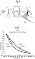
- a collimated light source from a lamp 301 is chopped by a chopper 303 and then split by a beamsplitter 305 into a "reference" channel 311 and a "signal" channel 313 which goes through a prototype sample 307 in a quartz tube 315.
- Two filters 302a, 302b one in each channel are narrow bandpass filters which select the operating light energy (wavelength).
- a lock-in amplifier 304b monitors the sample signal via sample detector 308b, and lock-in amplifier 304a reads the reference signal received via reference detector 308a.
- the signal S through the cathode and R through the reference are constantly compared to each other. The transmission is then simply the ratio of S to R.
- Oven temperature is monitored by a thermocouple 306.
- the sample, in oven enclosure 317 is at the temperature indicated by the thermocouple.
- a typical calibration curve is shown in Figure 4, where the transmission was taken to be unity at room temperature.
- the scheme illustrated in Figure 3 embodies a generic approach to measure the sample's temperature by the transmission method, resulting in the curve of Figure 4.
- a specific utilisation of this device is to monitor the temperature of a GaAs layer on a photocathode during "heat cleaning", or the temperature of a wafer (such as GaAs) during “heat cleaning” prior to growing epitaxial layers on the GaAs, for instance by the Molecular Beam Epitaxy method.
- the source of the light used to measure transmission through the sample may conveniently be the same source used to heat the sample. Consequently, the careful monitoring of the light-source intensity, which changes during the heat-cleaning cycle, is essential.
- FIG. 5 The use of the invention in "heat cleaning" a photocathode sample 503 is shown in Figure 5.
- a lamp 504 and the cathode 503 are shown within a vacuum chamber 500.
- a sample channel 505 and the reference channel 506 are compared for normalisation purposes.
- Each channel has a focusing lens 510,511, a narrow pass filter of 0.05 »m 512,513, a broad band silicon pin detector 514,515 and a current meter 516,517.
- the reference channel 506 has a neutral density filter 518 before its focusing lens 511.
- the cathode 503 is then moved into the path of the light at position 502, and a "room temperature reference signal" is taken, with the heating lamp at a sufficiently low intensity so as not to heat the cathode during this step.
- the "heat cleaning" cycle proceeds as the lamp intensity is increased.
- the signals from the two channels are acquired by a computer, not shown, through two inputs of an A/D converter, not shown, and they are constantly compared to provide a normalised (to constant optical flux) transmission profile which is converted to a temperature profile according to the calibration of Figure 4.
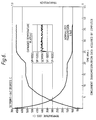
- a typical "heat cleaning" process monitored in accordance with the invention is shown in Figure 6.
- the transmission is seen to decrease as time goes on, due to the increase of the temperature of the cathode's active layer.
- the corresponding temperature can be deduced from Figure 4 and incorporated into software which is used to provide the plots similar to those shown in Figure 6.
- a time-dependent temperature profile can be entered into the software, and the transmission would act as a thermometer which reads the real-time temperature and compares it (at frequent intervals) to the above "dialed-in” temperature.
- Figure 6 as an example, are seen two time plots: the nominal faceplate temperature read by the IRCON, and the cathode temperature indicated by the transmission through the cathode [in Figure 6, the transmission values were not converted to cathode temperature; this would be done by using data at Figure 4].
- the software to control the heat clean process is written in a version of BASIC designed for measurement and control purposes.
- the program uses the multitasking capability of this language to measure and control the process and to provide screen display, data storage and data printout.
- the heat clean lamp With the cathode in the heat clean position, the heat clean lamp is operated briefly at low wattage. During this time, sampling measurements are made over a narrow wavelength band of light flux through the cathode and of light flux from the lamp. From these measurements a "room temperature" normalisation ratio is computed. Subsequent measurements of transmission through the cathode are divided by this number to normalise the transmission to the room temperature value.
- the heat clean process is begun.
- the computer periodically samples light flux from the lamp and through the cathode and calculates the transmission relative to the room temperature transmission. This value is compared to a setpoint value determined from a specified transmission versus time profile.
- the program is structured to readily accommodate changes in the desired shape and complexity of this curve. Using a PID (proportional-integral-derivative) algorithm, a correction to the lamp wattage is calculated and a corresponding command voltage is sent to the power supply controlling the lamp. This sequence is periodically repeated until the heat clean process is completed.
- PID proportional-integral-derivative
- Figure 7 One way of implementing the invention is shown in Figure 7 which utilises an arrangement where a single lens reflex camera having a lens 711 is used to focus a lamp filament 713, viewed through a cathode 715 in a vacuum chamber onto the surface of a detector 717 which is in the camera's focal plane.
- FIG 8. An expanded version of the invention is illustrated in Figure 8.
- the temperature of a sample 91 is monitored by measuring the optical transmission properties of a group of wavelengths (all corresponding to optical energies slightly above the bandgap).
- the source of optical radiation is a heat clean bulb 90 which is aligned with a plurality of slits 92a,92b arranged to substantially collimate the light.
- the sample 91 which comprises a layer 901 of a material having a direct bandgap which varies as a function of temperature, GaAs in this example, is placed so as to intercept the light between the bulb 90 and the slits 92.
- the light passing through the slits 92 has traversed the layer 901 of GaAs.
- a diffraction grating 93 a holographic, blazed grating in this example, is placed at an angle to the collimated light beam exiting slits 92 such that the light is dispersed, in a dispersed beam 94, onto an optical detector 95 which in this example is a linear detector array.
- the low frequency cutoff 96 is detected by the optical detector thus permitting the temperature detection according to the procedures described in connection with the prior examples. Additional benefits can be obtained by the use of a detector capable of isolating a pluraltiy of discrete wavelengths of optical energy. Since the functional dependence of ⁇ on (h ⁇ -Eg) [see Eq.
- This method, and the device are applicable to measure the temperatures of any semiconductor wafers or thin layers wherein the bandgap, and therefore the transmission, is temperature dependent.
- the method is usually limited to that layer with the narrowest bandgap.
- the method requires a light source emitting an optical component which is only partly absorbed in the sample.
- the method is particularly applicable to monitoring the temperature, in the manner indicated, in those processes wherein the optical source acts as the heating source.
- the method not only monitors and controls the temperature during the heating and "high temperature soak” (at a preset temperature) part of the cycle (see Figure 6), but it also monitors the cooling rate of the sample and determines when the sample has cooled down to a preset temperature.
Landscapes
- Physics & Mathematics (AREA)
- General Physics & Mathematics (AREA)
- Investigating Or Analysing Materials By Optical Means (AREA)
- Measuring Temperature Or Quantity Of Heat (AREA)
- Testing Or Measuring Of Semiconductors Or The Like (AREA)
- Light Receiving Elements (AREA)
Claims (14)
- Vorrichtung zur Temperaturerfassung, die ein Materialstück umfaßt, das eine Bandabstandsenergie hat, die als eine Funktion der Temperatur variiert, und die weiterhin eine Quelle optischer Energie zum Erzeugen optischer Energie zum Hindurchschicken durch das Stück und eine Detektionseinrichtung für das Messen der von dem Stück emittierten Energie umfaßt, dadurch gekennzeichnet, daß beim Gebrauch der Vorrichtung das Materialstück, das eine Bandabstandsenergie aufweist, ein Werkstück (307, 503, 901) bildet, dessen Temperatur zu bestimmmen ist, daß die Quelle der optischen Energie (301, 504, 90) eine erste spektrale Komponente mit einer Photonenenergie aufweist, die ein wenig größer als die Bandabstandsenergie bei einer gegebenen Werkstücktemperatur ist, daß eine Einrichtung (302 b) zur Auswahl eines schmalbandigen Spektralbereichs vorgesehen ist, der die erste spektrale Komponente enthält, daß die Detektionseinrichtung (308b, 515, 95) zum Messen der ersten spektralen Komponente der optischen Energie der Quelle dient, daß die Vorrichtung zum Positionieren des Werkstücks zwischen der Quelle und der Detektionseinrichtung geeignet ist, wodurch optische Energie durch das Werkstück gelangt, bevor die Messung der ersten spektralen Komponente der optischen Energie mittels der Detektionseinrichtung erfolgt, ohne daß ein physischer Kontakt mit irgendeiner die optische Energie transmittierenden Festkörpereinrichtung hergestellt wird, und daß eine Verarbeitungseinrichtung für das Empfangen eines Signals von der Detektionseinrichtung und für das Herstellen eines Ausgangssignals vorgesehen ist, welche die Temperatur des Werkstücks, wenn die Vorrichtung in Gebrauch ist, als eine Funktion des Energiewertes der optischen Energie, die durch das Werkstück absorbiert wird, anzeigt.
- Vorrichtung zur Temperaturerfassung nach Anspruch 1, dadurch gekennzeichnet, daß die Vorrichtung eine zweite optische Detektionseinrichtung (308a) aufweist, die optische Energie von der Quelle mißt und zum Empfangen optischer Energie, die nicht durch das Werkstück gelangt ist, angeordnet ist, wobei die zweite optische Detektionseinrichtung (308a) ein Referenzsignal für die Verarbeitungseinrichtung erzeugt.
- Vorrichtung zur Temperaturerfassung nach Anspruch 1 oder 2, dadurch gekennzeichnet, daß die Vorrichtung ein Werkstück enthält, das eine Schicht (101) aus GaAs umfaßt.
- Vorrichtung zur Temperaturerfassung nach Anspruch 3, dadurch gekennzeichnet, daß sich die Schicht aus GaAs auf einem Substrat (107) befindet.
- Vorrichtung zur Temperaturerfassung nach Anspruch 4, dadurch gekennzeichnet, daß das Substrat eine Glasschicht umfaßt.
- Vorrichtung zur Temperaturerfassung nach Anspruch 5, dadurch gekennzeichnet, daß die Glasschicht eine Planscheibe aus Glas ist.
- Vorrichtung zur Temperaturerfassung nach Anspruch 6, dadurch gekennzeichnet, daß sich eine Schicht (103) aus GaAlAs zwischen der Schicht (1010) aus GaAs und der Planscheibe aus Glas (107) befindet.
- Vorrichtung zur Temperaturerfassung nach Anspruch 7, dadurch gekennzeichnet, daß die Schicht (101) aus GaAs sich direkt auf der Schicht (103) aus GaAlAs befindet und die GaAlAs-Schicht auf der Planscheibe (107) aus Glas angeordnet ist.
- Vorrichtung zur Temperaturerfassung nach einem der vorhergehenden Ansprüche, dadurch gekennzeichnet, daß die Quelle optischer Energie (504) eine Wärmequelle ist, die thermisch mit dem Werkstück gekopppelt ist.
- Vorrichtung zur Temperaturerfassung nach Anspruch 9, dadurch gekennzeichnet, daß die Wärmequelle (301,504) eine weißglühende Lampe ist, die "weißes Licht" emittiert.
- Vorrichtung zur Temperaturerfassung, die ein Materialstück umfaßt, das eine Bandabstandsenergie aufweist, die als eine Funktion der Temperatur variiert, und die weiterhin eine Quelle optischer Energie zum Erzeugen optischer Energie zum Hindurchschicken durch das Stück und eine Detektionseinrichtung für das Messen der von dem Stück emittierten Energie umfaßt, dadurch gekennzeichnet, daß das Bandabstandsmaterial des Stücks eine erste Bandabstandsenergie bei einer interessierenden Temperatur aufweist, daß das Stück ein Werkstück (307) der Vorrichtung, während sie in Gebrauch ist, bildet, daß die Quelle der optischen Energie (301) eine erste spektrale Komponente einschließt, die eine Photonenenergie ein wenig größer als die erste Bandabstandsenergie aufweist, daß eine Einrichtung (302b) zur Auswahl eines schmalbandigen Spektralbereichs vorgesehen ist, der die erste spektrale Komponente enthält, daß die Detektionseinrichtung einen optischen Probendetektor (308b) für das Messen der Amplitude der ersten spektralen Komponente der optischen Energie und für das Erzeugen eines ersten für die gemessene Amplitude der ersten spektralen Komponente repräsentativen Signals umfaßt, daß die Vorrichtung zum Positionieren des Bandabstandsmaterials des Werkstücks zwischen der Quelle der optischen Energie (301) und dem optischen Probendetektor (308b) geeignet ist, ohne daß ein physischer Kontakt zwischen dem Werkstück und einem optischen Übertragungselement hergestellt wird, um die erste spektrale Komponente der optischen Energie durch das Bandabstandsmaterial des Werkstücks hindurchschicken und zum optischen Probendetektor (308b) übertragen zu lassen, daß eine Einrichtung (301) zum Heizen des Bandabstandsmaterials vorgesehen ist, daß ein optischer Referenzdetektor (308a) für das Messen der ersten spektralen Komponente der optischen Energie und für das Erzeugen eines zweiten für die gemessene Amplitude der ersten spektralen Komponente repräsentativen Signals vorgesehen ist und daß eine Vergleichseinrichtung zum Vergleichen des ersten und des zweiten für die gemessene Amplitude der ersten spektralen Komponente repräsentativen Signals und zur Erzeugung eines für die Temperatur des Bandabstandsmaterials des Werkstücks repräsentativen Signals, das auf dem Vergleich basiert, vorgesehen ist.
- Vorrichtung zur Temperaturerfassung nach Anspruch 11, dadurch gekennzeichnet, daß das für die Temperatur des Bandabstandsmaterials repräsentative Signal, das auf dem Vergleich basiert, als ein Rückkopplungseingangssignal für die Einrichtung (301) zum Heizen des Bandabstandsmaterials vorgesehen ist.
- Vorrichtung zur Temperaturerfassung nach Anspruch 11, dadurch gekennzeichnet, daß die Einrichtung zum Heizen des Bandabstandsmaterials die Quelle für die optische Energie (301) umfaßt.
- Vorrichtung zur Temperaturerfassung nach Anspruch 13, dadurch gekennzeichnet, daß die Quelle der optischen Energie eine weißglühende Lampe (301) ist.
Applications Claiming Priority (2)
| Application Number | Priority Date | Filing Date | Title |
|---|---|---|---|
| US157196 | 1988-02-17 | ||
| US07/157,196 US4890933A (en) | 1988-02-17 | 1988-02-17 | Transmission method to determine and control the temperature of wafers or thin layers with special application to semiconductors |
Publications (3)
| Publication Number | Publication Date |
|---|---|
| EP0329447A2 EP0329447A2 (de) | 1989-08-23 |
| EP0329447A3 EP0329447A3 (en) | 1990-05-16 |
| EP0329447B1 true EP0329447B1 (de) | 1994-06-29 |
Family
ID=22562716
Family Applications (1)
| Application Number | Title | Priority Date | Filing Date |
|---|---|---|---|
| EP89301517A Expired - Lifetime EP0329447B1 (de) | 1988-02-17 | 1989-02-16 | Vorrichtung für die Determination der Temperatur von Wafern oder Dünnschichten |
Country Status (4)
| Country | Link |
|---|---|
| US (1) | US4890933A (de) |
| EP (1) | EP0329447B1 (de) |
| JP (1) | JPH0214543A (de) |
| DE (1) | DE68916447T2 (de) |
Families Citing this family (20)
| Publication number | Priority date | Publication date | Assignee | Title |
|---|---|---|---|---|
| US5098199A (en) * | 1988-02-17 | 1992-03-24 | Itt Corporation | Reflectance method to determine and control the temperature of thin layers or wafers and their surfaces with special application to semiconductors |
| US5258602A (en) * | 1988-02-17 | 1993-11-02 | Itt Corporation | Technique for precision temperature measurements of a semiconductor layer or wafer, based on its optical properties at selected wavelengths |
| GB2238868A (en) * | 1989-11-22 | 1991-06-12 | Res Corp Technologies Inc | Silicon wafer temperature measurement by optical transmission monitoring. |
| US5118200A (en) * | 1990-06-13 | 1992-06-02 | Varian Associates, Inc. | Method and apparatus for temperature measurements |
| US5213985A (en) * | 1991-05-22 | 1993-05-25 | Bell Communications Research, Inc. | Temperature measurement in a processing chamber using in-situ monitoring of photoluminescence |
| US5313044A (en) * | 1992-04-28 | 1994-05-17 | Duke University | Method and apparatus for real-time wafer temperature and thin film growth measurement and control in a lamp-heated rapid thermal processor |
| US5773316A (en) * | 1994-03-11 | 1998-06-30 | Fujitsu Limited | Method and device for measuring physical quantity, method for fabricating semiconductor device, and method and device for measuring wavelength |
| US5772323A (en) * | 1994-10-26 | 1998-06-30 | Felice; Ralph A. | Temperature determining device and process |
| US6349270B1 (en) * | 1999-05-27 | 2002-02-19 | Emcore Corporation | Method and apparatus for measuring the temperature of objects on a fast moving holder |
| US20020147510A1 (en) * | 2001-01-29 | 2002-10-10 | Francis Robert Henry | Process for rapidly controlling a process variable without overshoot using a time domain polynomial feedback controller. |
| US6563092B1 (en) | 2001-11-28 | 2003-05-13 | Novellus Systems, Inc. | Measurement of substrate temperature in a process chamber using non-contact filtered infrared pyrometry |
| US7734439B2 (en) | 2002-06-24 | 2010-06-08 | Mattson Technology, Inc. | System and process for calibrating pyrometers in thermal processing chambers |
| US7543981B2 (en) | 2006-06-29 | 2009-06-09 | Mattson Technology, Inc. | Methods for determining wafer temperature |
| DE102007035609B4 (de) * | 2007-07-30 | 2021-09-16 | Ivoclar Vivadent Ag | Verfahren zur optischen Kontrolle des Verlaufs von einem auf einer Oberfläche eines Körpers erfolgenden physikalischen und/oder chemischen Prozesses |
| DE102007042779B4 (de) | 2007-09-07 | 2009-07-09 | Mattson Thermal Products Gmbh | Kalibrationssubstrat und -verfahren |
| US7976216B2 (en) * | 2007-12-20 | 2011-07-12 | Mattson Technology, Inc. | Determining the temperature of silicon at high temperatures |
| WO2009119367A1 (ja) * | 2008-03-28 | 2009-10-01 | コニカミノルタセンシング株式会社 | 分光特性測定システム、分光特性測定器、データ処理装置およびプログラム |
| US8673656B2 (en) * | 2008-12-26 | 2014-03-18 | Ysystems, Ltd. | Method and device for measuring temperature during deposition of semiconductor |
| WO2010148385A2 (en) * | 2009-06-19 | 2010-12-23 | K-Space Associates, Inc. | Thin film temperature measurement using optical absorption edge wavelength |
| US11359972B2 (en) * | 2020-09-15 | 2022-06-14 | Applied Materials, Inc. | Temperature calibration with band gap absorption method |
Citations (1)
| Publication number | Priority date | Publication date | Assignee | Title |
|---|---|---|---|---|
| EP0248111A2 (de) * | 1986-04-08 | 1987-12-09 | CV Technology, Incorporated | Spektralverfahren und -vorrichtung zum optischen Messen der Temperatur |
Family Cites Families (11)
| Publication number | Priority date | Publication date | Assignee | Title |
|---|---|---|---|---|
| DE1811022C3 (de) * | 1968-11-26 | 1978-04-27 | Institut Metallurgii Im. A.A. Bajkowa, Moskau | Einrichtung zur Regelung der Farbtemperatur eines Objektes mittels zwei Strahlungsstromen |
| US3672221A (en) * | 1969-12-19 | 1972-06-27 | Monsanto Co | Temperature sensor |
| US4302970A (en) * | 1980-05-09 | 1981-12-01 | United Technologies Corporation | Optical temperature probe employing rare earth absorption |
| SE423752B (sv) * | 1980-09-29 | 1982-05-24 | Asea Ab | Optiskt sensorelement |
| DE3202981A1 (de) * | 1982-01-29 | 1983-08-11 | Eugen 7547 Wildbad Riexinger | Vorrichtung zum aufheizen des endes eines kunststoffrohres, insbesondere aus vernetztem polyaethylen |
| JPS59111027A (ja) * | 1982-12-17 | 1984-06-27 | Fuji Electric Corp Res & Dev Ltd | 温度測定方法 |
| GB8418063D0 (en) * | 1984-07-16 | 1984-08-22 | Atomic Energy Authority Uk | Temperature control in vacuum |
| JPS6154184A (ja) * | 1984-08-22 | 1986-03-18 | 株式会社チノー | 加熱処理装置 |
| KR900005778B1 (ko) * | 1984-10-17 | 1990-08-11 | 미쓰비시전기 주식회사 | 온도측정장치 |
| JPS61228637A (ja) * | 1985-04-01 | 1986-10-11 | Dainippon Screen Mfg Co Ltd | 温度測定装置を付設した加熱装置 |
| US4708677A (en) * | 1985-12-27 | 1987-11-24 | Itt Electro Optical Products, A Division Of Itt Corporation | Method of measuring the temperature of a photocathode |
-
1988
- 1988-02-17 US US07/157,196 patent/US4890933A/en not_active Expired - Fee Related
-
1989
- 1989-02-16 DE DE68916447T patent/DE68916447T2/de not_active Expired - Fee Related
- 1989-02-16 EP EP89301517A patent/EP0329447B1/de not_active Expired - Lifetime
- 1989-02-16 JP JP1035184A patent/JPH0214543A/ja active Pending
Patent Citations (1)
| Publication number | Priority date | Publication date | Assignee | Title |
|---|---|---|---|---|
| EP0248111A2 (de) * | 1986-04-08 | 1987-12-09 | CV Technology, Incorporated | Spektralverfahren und -vorrichtung zum optischen Messen der Temperatur |
Also Published As
| Publication number | Publication date |
|---|---|
| DE68916447T2 (de) | 1994-10-13 |
| EP0329447A3 (en) | 1990-05-16 |
| EP0329447A2 (de) | 1989-08-23 |
| DE68916447D1 (de) | 1994-08-04 |
| US4890933A (en) | 1990-01-02 |
| JPH0214543A (ja) | 1990-01-18 |
Similar Documents
| Publication | Publication Date | Title |
|---|---|---|
| US4890933A (en) | Transmission method to determine and control the temperature of wafers or thin layers with special application to semiconductors | |
| US5098199A (en) | Reflectance method to determine and control the temperature of thin layers or wafers and their surfaces with special application to semiconductors | |
| US5118200A (en) | Method and apparatus for temperature measurements | |
| US5180226A (en) | Method and apparatus for precise temperature measurement | |
| US5568978A (en) | Optical apparatus and method for measuring temperature of a substrate material with a temperature dependent band gap | |
| US5439291A (en) | Method and apparatus for AC Differential thermal analysis | |
| US5229303A (en) | Device processing involving an optical interferometric thermometry using the change in refractive index to measure semiconductor wafer temperature | |
| US5170041A (en) | Transmission method to determine and control the temperature of wafers or thin layers with special application to semiconductors | |
| US5258602A (en) | Technique for precision temperature measurements of a semiconductor layer or wafer, based on its optical properties at selected wavelengths | |
| CN105136310B (zh) | Mocvd外延片表面温度测量的紫外测温方法及装置 | |
| EP0429081A2 (de) | Temperaturmessung an einer Siliciumplaquette durch Erfassung der optischen Transmission | |
| US5167452A (en) | Transmission method to determine and control the temperature of wafers or thin layers with special application to semiconductors | |
| JP2000516038A (ja) | 改良された温度感知および監視を含む短時間アニールシステムおよびその方法 | |
| JPH1062238A (ja) | 光学スペクトロメータ | |
| Jackson et al. | In situ monitoring and control for MBE growth of optoelectronic devices | |
| Mullins et al. | High temperature optical properties of cadmium telluride | |
| Wang et al. | Real-time, noninvasive temperature control of wafer processing based on diffusive reflectance spectroscopy | |
| US7129168B2 (en) | Method of estimating substrate temperature | |
| EP0961310A2 (de) | Verbesserte Temperaturregelung für eine Vorrichtung zur Behandlung von Siliziumbauelementen | |
| Sitter et al. | Exact determination of the real substrate temperature and film thickness in vacuum epitaxial growth systems by visible laser interferometry | |
| Jensen et al. | Integrated multi-sensor control of II–VI MBE for growth of complex IR detector structures | |
| Aleksandrov et al. | Pyrometer unit for gaas substrate temperature control in an mbe system | |
| Bertness | Smart pyrometry for combined sample temperature and reflectance measurements in molecular-beam epitaxy | |
| JPH0493730A (ja) | 温度測定装置 | |
| Nason et al. | In situ temperature measurement of α‐mercuric iodide by reflection spectroscopy |
Legal Events
| Date | Code | Title | Description |
|---|---|---|---|
| PUAI | Public reference made under article 153(3) epc to a published international application that has entered the european phase |
Free format text: ORIGINAL CODE: 0009012 |
|
| AK | Designated contracting states |
Kind code of ref document: A2 Designated state(s): DE FR GB NL |
|
| PUAL | Search report despatched |
Free format text: ORIGINAL CODE: 0009013 |
|
| AK | Designated contracting states |
Kind code of ref document: A3 Designated state(s): DE FR GB NL |
|
| 17P | Request for examination filed |
Effective date: 19900813 |
|
| 17Q | First examination report despatched |
Effective date: 19911029 |
|
| GRAA | (expected) grant |
Free format text: ORIGINAL CODE: 0009210 |
|
| AK | Designated contracting states |
Kind code of ref document: B1 Designated state(s): DE FR GB NL |
|
| REF | Corresponds to: |
Ref document number: 68916447 Country of ref document: DE Date of ref document: 19940804 |
|
| ET | Fr: translation filed | ||
| PLBE | No opposition filed within time limit |
Free format text: ORIGINAL CODE: 0009261 |
|
| STAA | Information on the status of an ep patent application or granted ep patent |
Free format text: STATUS: NO OPPOSITION FILED WITHIN TIME LIMIT |
|
| 26N | No opposition filed | ||
| PGFP | Annual fee paid to national office [announced via postgrant information from national office to epo] |
Ref country code: NL Payment date: 19980121 Year of fee payment: 10 Ref country code: FR Payment date: 19980121 Year of fee payment: 10 |
|
| PGFP | Annual fee paid to national office [announced via postgrant information from national office to epo] |
Ref country code: DE Payment date: 19980123 Year of fee payment: 10 |
|
| PGFP | Annual fee paid to national office [announced via postgrant information from national office to epo] |
Ref country code: GB Payment date: 19980127 Year of fee payment: 10 |
|
| PG25 | Lapsed in a contracting state [announced via postgrant information from national office to epo] |
Ref country code: GB Free format text: LAPSE BECAUSE OF NON-PAYMENT OF DUE FEES Effective date: 19990216 |
|
| PG25 | Lapsed in a contracting state [announced via postgrant information from national office to epo] |
Ref country code: NL Free format text: LAPSE BECAUSE OF NON-PAYMENT OF DUE FEES Effective date: 19990901 |
|
| GBPC | Gb: european patent ceased through non-payment of renewal fee |
Effective date: 19990216 |
|
| PG25 | Lapsed in a contracting state [announced via postgrant information from national office to epo] |
Ref country code: FR Free format text: LAPSE BECAUSE OF NON-PAYMENT OF DUE FEES Effective date: 19991029 |
|
| PG25 | Lapsed in a contracting state [announced via postgrant information from national office to epo] |
Ref country code: DE Free format text: LAPSE BECAUSE OF NON-PAYMENT OF DUE FEES Effective date: 19991201 |
|
| REG | Reference to a national code |
Ref country code: FR Ref legal event code: ST |