EP0329793B1 - Circuit electronique a haute vitesse presentant une configuration cascode - Google Patents
Circuit electronique a haute vitesse presentant une configuration cascode Download PDFInfo
- Publication number
- EP0329793B1 EP0329793B1 EP88906881A EP88906881A EP0329793B1 EP 0329793 B1 EP0329793 B1 EP 0329793B1 EP 88906881 A EP88906881 A EP 88906881A EP 88906881 A EP88906881 A EP 88906881A EP 0329793 B1 EP0329793 B1 EP 0329793B1
- Authority
- EP
- European Patent Office
- Prior art keywords
- load
- transistor
- circuit
- transistors
- current source
- Prior art date
- Legal status (The legal status is an assumption and is not a legal conclusion. Google has not performed a legal analysis and makes no representation as to the accuracy of the status listed.)
- Expired - Lifetime
Links
Images







Classifications
-
- H—ELECTRICITY
- H03—ELECTRONIC CIRCUITRY
- H03K—PULSE TECHNIQUE
- H03K5/00—Manipulating of pulses not covered by one of the other main groups of this subclass
- H03K5/15—Arrangements in which pulses are delivered at different times at several outputs, i.e. pulse distributors
-
- H—ELECTRICITY
- H03—ELECTRONIC CIRCUITRY
- H03F—AMPLIFIERS
- H03F1/00—Details of amplifiers with only discharge tubes, only semiconductor devices or only unspecified devices as amplifying elements
- H03F1/08—Modifications of amplifiers to reduce detrimental influences of internal impedances of amplifying elements
- H03F1/22—Modifications of amplifiers to reduce detrimental influences of internal impedances of amplifying elements by use of cascode coupling, i.e. earthed cathode or emitter stage followed by earthed grid or base stage respectively
-
- H—ELECTRICITY
- H03—ELECTRONIC CIRCUITRY
- H03F—AMPLIFIERS
- H03F3/00—Amplifiers with only discharge tubes or only semiconductor devices as amplifying elements
- H03F3/45—Differential amplifiers
- H03F3/45071—Differential amplifiers with semiconductor devices only
- H03F3/45076—Differential amplifiers with semiconductor devices only characterised by the way of implementation of the active amplifying circuit in the differential amplifier
- H03F3/4508—Differential amplifiers with semiconductor devices only characterised by the way of implementation of the active amplifying circuit in the differential amplifier using bipolar transistors as the active amplifying circuit
- H03F3/45085—Long tailed pairs
- H03F3/45089—Non-folded cascode stages
-
- H—ELECTRICITY
- H03—ELECTRONIC CIRCUITRY
- H03K—PULSE TECHNIQUE
- H03K19/00—Logic circuits, i.e. having at least two inputs acting on one output; Inverting circuits
- H03K19/0175—Coupling arrangements; Interface arrangements
- H03K19/018—Coupling arrangements; Interface arrangements using bipolar transistors only
- H03K19/01806—Interface arrangements
-
- H—ELECTRICITY
- H03—ELECTRONIC CIRCUITRY
- H03K—PULSE TECHNIQUE
- H03K19/00—Logic circuits, i.e. having at least two inputs acting on one output; Inverting circuits
- H03K19/0175—Coupling arrangements; Interface arrangements
- H03K19/018—Coupling arrangements; Interface arrangements using bipolar transistors only
- H03K19/01825—Coupling arrangements, impedance matching circuits
Definitions
- the present invention relates to an electronic circuit having a cascode configuration. More particularly, it relates to an electronic circuit able to operate at a high speed and/or having a wide frequency band.
- Recent technology advances in data processing systems require improved electronic circuits able to process data at a high speed and/or at a wide frequency band.
- a very high speed data transmission of more than 1.6 giba-bits per second (Gbs) has been attempted, to increase a transmission rate to a propagation speed limit of an optical fiber cable which has a very wide frequency range.
- JP-A-6059813 describes a latched comparator including a voltage comparator having two input transistors whose emitters are commonly connected and operatively grounded. The collectors of the transistors are connected to load resistors respectively via switching transistors. The emitters of switching transistors are connected to the collectors of the input transistors and the collectors of the switching transistors are connected to the load transistors.
- An object of the present invention is to provide an improved electronic circuit having a high speed operation time, a wide frequency range and/or a great stability.
- Another object of the present invention is to provide an improved level shift circuit able to operate at a high speed.
- Still another object of the present invention is to provide an improved level shift circuit having a great stability at a high frequency range.
- Yet another object of the present invention is to provide an improved discrimination circuit able to discriminate a signal level with a high accuracy.
- Another object of the present invention is to provide an improved signal synthesization circuit having many fan-ins.
- a level shift circuit comprising: a current drive circuit including at least one input transistor, the emitter thereof being operatively grounded and a base thereof receiving a respective input signal; a load transistor circuit including at least one load transistor, the base of each load transistor being operatively grounded, the emitter of each load transistor being connected to the collector of a respective input transistor; a bias current source connected between said emitter of said load transistor and ground, a respective current generated by said bias current source being supplied to each load transistor to maintain a forward base emitter voltage of each load transistor; and a load resistor circuit including at least one load resistor connected between the collector of a respective load transistor in said load transistor circuit and a power supply voltage, an output signal being provided at the collector of each load transistor; characterized in that said bias current source comprises a current mirror circuit for each current to be provided, at least one of said current mirror circuits being connected to a control voltage source to shift the level of said output signal by a value defined by the control voltage source.
- said current drive circuit includes first and second input transistors connected in parallel to differentially operate in response to two input signals connected to bases thereof and a current source connected between emitters of said first and second input transistors and ground
- said load transistor circuit includes first and second load transistors, the emitter of said first load transistor being connected to the collector of said first input transistor, the emitter of said second load transistor being connected to the collector of said second input transistor and bases of said first and second load transistors being commonly connected and operatively grounded
- said load resistor circuit includes two load resistors connected to collectors of said first and second load transistors, respectively, to output two output signals from points at which said collectors and said load resistors are commonly connected
- said current-mirror circuit includes first to third current source transistors connected in parallel, collectors of said first and second current source transistors being respectively connected to said emitters of said first and second load transistors, the control voltage source being connected to a collector of said third current source transistor, the collector of said third current source transistor being connected to a base thereof which is commonly connected
- a latch circuit is connected to said load resistor circuit.
- Such a circuit can operate as a signal discrimination circuit.
- said current drive circuit includes first and second input transistors connected in parallel to differentially operate in response to two input signals connected to bases thereof and a current source connected between emitters of said first and second input transistors and ground
- said load transistor circuit includes first and second load transistors, the emitter of said first load transistor being connected to the collector of said first input transistor, the emitter of said second load transistor being connected to the collector of said second input transistor and bases of said first and second load transistors being commonly connected and operatively grounded
- said load resistor circuit includes two load resistors connected to collectors of said first and second load transistors, respectively, to output two output signals from points at which said collectors and said load resistors are commonly connected
- said bias current source includes the first and a second current mirror circuit connected to said first and second load transistors, respectively.
- a plurality of said current drive circuits are connected in parallel, each current drive circuit receiving a said input signal to be synthesized, said bias current source and said emitter of said at least one load transistor in said load transistor circuit are connected to the commonly connected collectors of said parallel current drive circuits.
- Such a circuit can be used as a signal synthesizing circuit.
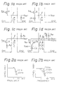
- Figures 1a to 1d show prior art interface circuits.
- Figure 1a shows an open-emitter type interface circuit
- Fig. 1b shows an emitter-follower type interface circuit
- Fig. 1c shows an open-collector type interface circuit
- Fig. 1d shows a differential-operation and open-collector type interface circuit.
- reference CH1 denotes a transmission side integrated circuit (IC) chip
- CH2 denotes a reception side IC chip
- Q, Q1 and Q2 denote npn-type transistors
- R, R11 and R12 denote resistors
- CS denotes a constant current source
- C, C1 and C2 denote stray capacitors.
- the IC chip CH1 is provided at a data transmission side
- the IC chip CH2 is provided at a data reception side
- the data transmission line(s) l or l1 and l2 is (are) provided therebetween.
- the stray capacitor(s) C or C1 and C2 may be connected to the data transmission line(s) l or l1 and l2.
- the open-emitter type interface circuit shown in Fig. 1a is a voltage signal propagation type interface circuit.
- An input impedance of the transmission side IC chip CH1 is low, and an input impedance of the reception side IC chip IC2 is high.
- Figure 2a shows a frequency characteristic of the open-type interface circuit shown in Fig. 1a.
- curve CV1 a shows a frequency characteristic when the stray capacitance C S is 0.5 pF
- curve CV1 b shows a frequency characteristic when the stray capacitance C S is 5 pF. Since the emitter resistance r E is small, an affect due to the stray capacitor is reduced and a frequency band where a gain is lowered by 3 dB is broad, but a distortion, such as peaking occurs.
- the emitter-follower type interface circuit shown in Fig. 1b also suffers from the above defect.
- f -3dB 1 2 R L ⁇ C S
- R L represents a resistance of the load resistor(s) R1 or R11 and R12.
- Figure 2b shows a frequency characteristic of the interface circuits shown in Figs. 1c and 1d.
- curves CV2 a , CV2 b , and CV2 c show frequency characteristics where the stray capacitance C S are 0.1 pF, 0.5 pF and 1.0 pF, respectively.
- the resistance R L of the load resistor(s) R1 or R11 and R12 can not be made too small because an output signal(s) S OUT or S OUT1 and S OUT2 having a predetermined amplitude must be provided, an affect due to the stray capacitance C S can not be eliminated, as shown in Fig. 2b.
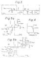
- Figure 3 shows a principle interface circuit, which comprises a current drive source ID in a transmission side IC chip CH1, and, an npn-type transistor Q in which a base is grounded and an emitter is connected to the current drive source ID through a transfer line l, and a load resistor R in a reception side IC chip CH2.
- a stray capacitor C may be connected to the transfer line l.
- C S is a capacitance of the stray capacitor C
- g m is a mutual conductance of the transistor Q.
- V OUT R L ⁇ 1 1 + jwC S g m I d
- a frequency f -3dB g m 2 ⁇ C S
- Figure 4 shows a graph of a frequency characteristic of the interface circuit shown in Fig 3.
- curves CV3 a and CV3 b show the frequency characteristics when the stray capacitances C S are 1 pF and 5 pF, respectively. More concretely, when a DC current component of the current drive source ID is 2 mA, a resistance: 1/g m is 13 ⁇ and, when the stray capacitance C S is 1 pF, the frequency f -3dB is 12 Giga-Hertz (GHz).
- this interface circuit shown in Fig. 3 is not substantially affected by the stray capacitance C S of approximately 1 pF on s signal transfer at approximately 10 GHz.
- FIG. 5a shows specific circuits of the interface circuit of shown in Fig. 3.
- the circuit shown in Fig. 5a comprises the current drive source ID consisting of an npn-type transistor Q1 and an emitter resistor R1 having a terminal connected to an emitter of the transistor Q1 and another terminal connected to a low voltage supply V EE which may be ground.
- the circuit also comprises an npn-type transistor Q2 having an emitter connected to a collector of the transistor Q1 through the transfer line l and a base supplied with a bias voltage supply V B , and a load resistor R2 connected between a high voltage supply V CC and a collector of the transistor Q2.
- an input signal S IN is supplied to a base of the transistor Q1 , and at the IC chip CH2, an output signal S OUT is output from a point at which the load resistor R2 and the collector of the transistor Q2 are commonly connected.
- the stray capacitor C is connected to the transfer line l.
- the interface circuit shown in Fig. 5a is formed by a "cascode configuration", since the emitter of the transistor Q1 is grounded through the resistor R1 , the collector of the transistor Q1 and the emitter of the transistor Q2 are connected, and the base of the transistor Q2 is grounded through the bias voltage supply V B .
- a cascode amplifier having the above configuration is used for a high frequency amplification, because an input signal side and a load side are separated and an internal feedback is small, and thus a high speed operation can be established.
- a total gain of the cascode amplifier is equal to a gain of a load transistor, because a load at a first step is a resistor of an input transistor in the second step, i.e., an emitter resistance r E of the input transistor which is very small.
- a load at a first step is a resistor of an input transistor in the second step, i.e., an emitter resistance r E of the input transistor which is very small.
- r E of the input transistor which is very small.
- the current drive source ID is constructed by differential operation transistor pair Q11 and Q12 and a constant current source CS.
- the load (output) circuit also includes a pair of transistors Q21 and Q22 , a pair of load resistors R21 and R22 , and the bias voltage supply V B . Emitters of the transistors Q11 and Q12 are grounded through the constant current source CS, and bases of the transistors Q21 and Q22 are grounded through the bias voltage supply V B . Accordingly, this interface circuit shown in Fig. 5b has a cascode configuration.
- the interface circuit described in JPA 63-1211 still suffers from the affect of a large stray capacitance at a high frequency when the input signal S IN has a large amplitude, for example, 800 mV or more.
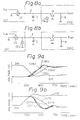
- Figures 6a and 6b show graphs of response characteristics of the interface circuit shown in Fig 3, obtained by simulation.
- Figure 6a shows rising wave forms of the output signal S OUT to a drive signal, i.e., the input signal S IN , represented by curve DW
- Fig. 6b shows trailing (falling) wave forms to the drive signal.
- curves CV4 a to CV4 d show rising wave forms of the output signal S OUT when the stray capacitances are 0.1 pF, 0.5 pF, 1.0 pF and 5.0 pF, respectively.
- the variation of rising times is small, but a large ringing appears due to the stray capacitance.
- curves CV5 a to CV5 d show trailing wave forms of the output signal S OUT when the stray capacitance are 0.0 pF, 0.1 pF, 0.5 pF and 1.0 pF, respectively.
- the start points of the trailing are greatly varied due to the stray capacitance, and the ringing is also large.
- the base ⁇ emitter voltage V BE of the load transistor Q is approximately 0.8 V.
- Figs. 8a and 8b eliminate the change of the transfer line voltage V l , and thus eliminate the charging and discharging of the stray capacitor C, to shorten the rising time and the trailing time.
- the interface circuit includes a current drive source ID in a transmission side IC chip CH1.
- the interface circuit also includes, at a reception side IC chip CH2, a load (output) transistor Q and a load resistor R. Between the chips CH1 and CH2, a transfer line l is provided, and a stray capacitor C can be connected to the transfer line l.
- the current drive circuit ID includes an input transistor (not shown), an emitter thereof being grounded. A base of the load transistor Q is connected to a collector of the input transistor, and a base thereof is grounded.
- the above circuit construction is substantially the same as that of the interface circuit shown in Fig. 3, and thus the interface circuit shown in Fig. 8a has a cascode configuration.
- the interface circuit shown in Fig. 8a includes a bias current source CS0 connected between the emitter and the base of the load transistor Q in the reception side IC chip CH2.
- the bias current source CS0 provides a constant current I CS corresponding to a current I BE flowing through the base and the emitter of the load transistor, i.e., the above on-current I ON , Q when the transistor Q is turned ON, for cancelling the current I BE .
- the constant current I CS has an amplitude sufficient to prevent the change of the voltage V l on the transfer line l, i.e., to prevent the change of the base-emitter voltage V BE of the load transistor and has a polarity which is the reserve of a polarity of the on current I ON .
- the constant current I CS generates a voltage between the base and the emitter of the transistor Q opposite to the base-emitter voltage V BE of the load transistor Q when the load transistor Q is turned ON.
- the constant current I CS may be 0.5 mA or higher. Taking a margin into consideration, the constant current I CS may be 0.5 mA.
- the bias current source CS0 always provides the constant current I CS to the load transistor Q to suppress the change of the base-emitter voltage V BE , so that the voltage V l on the transfer line l is not changed regardless of the change of the status of the load transistor Q, i.e., the change between the ON state and the OFF state, of the load transistor Q. Accordingly, the charging and discharging of the stray capacitor C are avoided, and generation of the distortion of the rising signal and the trailing signal is prevented.
- the bias current source CS0 can be provided at the transmission side IC chip CH1. Since the bias current source CS0 is connected between the base and the emitter of the load transistor Q, the operation is same to that described above.
- a DC level of the output signal S OUT can be made low than that of the interface circuit shown in Fig. 3, and thus the resistance R L of the load resistor R should be greater than that of the load resistor shown in Fig. 3.
- a current flowing through the load transistor Q may be increased, and a capacity of the load transistor Q may become larger than that of the transistor shown in Fig. 3.
- an amplitude of the output signal S OUT per se, is not changed, regardless of the provision of the bias current source CS0.
- Figures 9a and 9b show the characteristic curves of the interface circuits shown in Figs. 8a and 8b obtained by simulation.
- Figure 9a shows a rising characteristic.
- curves CV6 a to CV6 d represent the rising characteristics corresponding to the change of the drive signal, i.e., the input signal S IN , represented by curve DW, when the stray capacitances C S are 0.1 pF, 0.5 pF, 1.0 pF, and 5.0 pF.
- These curves CV6 a to CV6 d correspond to the curves CV4 a to CV4 d in Fig. 6a. Compared with these, as shown in Fig.
- the characteristics shown by the curves CV4 a to CV4 c when the stray capacitances are 0.1 pF, 0.5 pF, and 1.0 pF are greatly varied therebetween, but on the other hand, as shown in Fig. 9a, the characteristics shown by the curves CV6 a to CV6 c are not varied each other. This means that the transfer line l in the interface circuit shown in Fig. 8a can install at a short distance or a long distance without any circuit adjustment.
- the characteristics shown by the curves CV7 a to CV7 c mean the same thing.
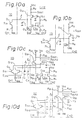
- Figures 10a to 10d show circuit diagrams of an interface circuit.
- the interface circuits shown in Figs. 10a and 10b are the open-collector type interface circuits corresponding to the interface circuit shown in Fig. 5a.
- the bias current source CS0 is formed by a current-mirror type current source composed of npn-type transistor Q3 and Q4 , resistors R3 and R4, and a resistor R5.
- the current-mirror type current source, per se, is well known.
- the bias current source CS0 is formed by a resistor R6.
- the interface circuits shown in Figs. 10c and 10d are differential-operation and open-collector type interface circuits corresponding to the interface circuit shown in Fig. 5b.
- the bias current source CS0 is formed by a current-mirror type constant current source composed of npn-type transistor Q31 , Q32 and Q4 , and resistors R31 , R32 , R4 and R5.
- the bias current source CS0 is formed by two resistors R61 and R62.
- the interface circuits shown in Figs. 10a to 10d can be provided with the bias current source CS0 at the transmission side IC chip CH1.
- the input signal S IN is a high frequency repetition signal, such as a clock signal, in the base-grounded interface circuit shown in Fig. 3, a wave form distortion may not occur, since a charge accumulated in the stray capacitor is not fully discharged, and the base emitter voltage V BE is not substantially changed.
- the input signal S IN is a data signal which may be formed by continuous one's data or continuous zero's data
- a wave form distortion can occur at a transient state where an end of the continuous one's data is followed by a first of the continuous zero's data, or vice versa.
- interface circuits are very useful when forming interfaces, such as an interface between circuits in a gate array integrated circuit chip wherein a wiring pattern capacitance is considerably large, and an interface between chips wherein a bonding pad capacitance can not be neglected.
- a level shift of a DC bias level of a signal by a predetermined voltage is required.
- a DC level of an input signal can be shifted to a level equal to a reference voltage by using the level shift circuit.
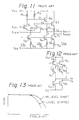
- FIG 11 shows a prior art differential-operation type level shift circuit.
- the level shift circuit includes a pair of differential-operation transistors Q1 and Q2 , a first current source CS1 consisting of a transistor Q3 and a resistor R3 , a second current source CS2 consisting of a transistor Q4 and a resistor R4 , a third current source CS3 consisting of a transistor Q5 and a resistor R5 , output emitter follower transistors Q6 and Q7 , and resistors R1 , R2 , R6 and R7.
- a pair of differential-operated output voltages V1 and V2 are respectively extracted from points at which collectors of the transistors Q1 and Q2 and the load resistors R1 and R2 are commonly connected, and supplied to bases of the transistors Q6 and Q7.
- Output signals S OUT1 and S OUT2 having voltages V3 and V4 , respectively, are output from points collectors of the transistors Q4 and Q5 and the resistors R6 and R7 are commonly connected.
- V2 V BE + I2R7 + V4
- V BE is a base-emitter voltage of the transistors Q4 and Q5
- R6 and R7 are resistances of the resistors R6 and R7
- I1 is a current passing through the transistor Q4
- I2 is a current passing through the transistor Q5.
- the output voltages V3 and V4 are shifted from the voltage V1 and V2 by (V BE + I1R6) and (V BE + I2R7).
- the levels to be shifted can be easily changed continuously by changing the currents I1 and I2 of the current sources CS2 and CS3.
- Figure 12 shows a prior art diode-type level shift circuit.
- n-series connected transistors for example, Q11 , each connected between a collector and a base and functioning as a diode, are connected between transistors Q6 and Q4.
- n-series connected transistors for example, Q21 , each connected between a collector and a base and functioning as a diode, are connected between transistors Q7 and Q5.
- V1 (n+1)V BE + V3
- V2 (n+1)V BE + V4
- V BE is a base-emitter voltage of the diode-functioning transistor.
- a level shift voltage (n+1)V BE can be stepwisely changed.
- Figure 13 shows a graph of frequency characteristics of the level shift circuits shown in Figs. 11 and 12.
- the frequency characteristic is reduced, and accordingly, a wave response characteristic is reduced.
- the level shift circuit shown in Fig. 12 has the same problem as that described above.
- a circuit providing a bias current source CS0 in addition to the cascode configuration as shown in Figs. 8a and 8b prevents a distortion of a wave form of a output signal and the reduction of a variety of characteristics, due to the stray capacitance.
- the above feature is included to form a high speed level shift circuit without the reduction of the frequency characteristic and the wave response characteristic.
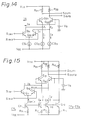
- Figure 14 shows a principle circuit diagram of a level shift circuit.
- the level shift circuit includes a pair of differential-operation transistors Q11 and Q12 , and a constant current source CS1 connected between collectors of the transistors Q11 and Q12 and a low voltage line V EE which may be ground.
- the level shift circuit also includes load resistors R21 and R22 , load transistors Q21 and Q22 , a bias voltage supply V B , and level shift current sources CS2 and CS3.
- the emitters of the transistors Q11 and Q12 are grounded through the constant current source CS1 , collectors of the transistors Q11 and Q12 are connected to emitters of the transistors Q21 and Q22 , and bases of the transistors Q21 and Q22 are grounded through the bias voltage supply V B . Accordingly, the above circuit has a cascode configuration.
- the variable current sources CS2 and CS2 corresponding to the bias current source CS0 shown in Fig. 8a are connected between the emitters of the transistors Q21 and Q22 and the low voltage line V EE , which is ground.
- a differential-operation pair circuit corresponding to the current drive circuit ID in Fig. 8a, consisting of the transistors Q11 and Q12 and the constant current sources CS1 receives voltage input signals S IN1 and S IN2 , and changes to currents I3 and I4 flowing therethrough. The currents I3 and I4 are varied in response to the voltages of the input signals S IN1 and S IN2 .
- the basic condition of the interface circuits shown in Figs. 8a and 8b and Figs. 10a to 10d can be applied to the level shift circuit shown in Fig. 14, except for the variable level shift current sources CS2 and CS3. Therefore, the features of the interface circuit are maintained in the level shift circuit.
- a basic difference between the interface circuit and the level shift circuit is the provision of the constant bias current source CS0 and the variable level shift current sources CS2 and CS3.
- the current sources CS2 and CS3 can be formed as constant current sources.
- Figure 15 shows a further circuit diagram of a level shift circuit
- the constant current source CS1 is composed of an npn-transistor Q3 and a resistor R3 , and supplies a current corresponding to (I3 + I4).
- the current sources CS2 and CS3 are formed by a current-mirror type current source circuit consisting of npn-type transistors Q4 , Q5 , and Q10 , and resistors R4 , R5 , R10 , and R11.
- the transistors Q4 and Q5 and the transistors R4 and R5 are defined to supply the current I1 and I2.
- the current sources CS2 and CS3 are constant current sources, and the level shift is fixed.
- a first embodiment of a level shift circuit in accordance with the present invention is shown, in which the current source CS1 consists of a transistor Q3 and a resistor R3 , the current source CS2 consists of a resistor R10 , a transistor Q10 , a resistor R11 , a transistor Q4 , and a resistor R4 , and the current source CS3 consists of a transistors Q5 and Q14 , and resistors R5 and R12.
- the current source CS2 and the current source CS3 are current-mirror type current sources.
- the level shift circuit in accordance with the second embodiment of the present invention is shown in Fig. 17 and is a modification of the level shift circuit shown in Fig. 16.
- the constant current source CS1 is formed by a current-mirror type current source consisting of a resistor R10 , transistors Q10 and Q3 , and resistors R11 and R3.
- the current sources CS2 and CS3 are formed by a variable current-mirror type current source consisting of transistors Q4 , Q5 , and Q14 , and resistors R4 , R5 and R12.
- the constant current source CS1 is formed by a current-mirror type current source consisting of transistors Q3 and Q10, and resistors R10, R3, and R11.
- the current sources CS2 and CS3 are variable resistors R4 and R5.
- the levels of both of the output signals S OUT1 and S OUT2 can be freely shifted by adjusting the resistances of the resistors R4 and R5.
- the signal discrimination circuit can be applied, for example, to a repeater in an optical data transmission system.
- a repeater in the repeater, as shown in Fig. 19, an optical to electrical (OE) converted signal is equalized and amplified at an equalizing amplifier 10, and a clock signal is extracted at a timing circuit 14.
- the equalized signal is discriminated by a timing signal from the timing circuit 14 at a signal discriminal circuit 12, and the discriminated signal is reproduced at a reproduction circuit 16.
- a discriminating level can be varied by adjusting a variable resistor R VR .
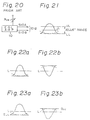
- the equalizing amplifier 10 outputs an equalized signal S10A and a discriminating threshold voltage signal S10B. As shown in Fig.
- the equalized signal S10A having a distorted eye-pattern by an optical shock and a shifted timing, is discriminated by a threshold level L at the discrimination circuit 12, and a high level signal is output when the equalized signal is higher than the threshold level L at a clock timing, and alternatively, a low level signal is output.
- the threshold level L is adjusted by the variable resistor R VR , and the discrimination circuit 12 discriminates the equalized signal S10A by using the adjusted threshold level signal S10B.
- a very high speed signal processing is required.
- Such a high speed signal processing requires an improvement of a wave form response and a prevention of cross-talk.
- the improvement and the prevention in general, require to reduce a gain at the equalizing amplifier, and to reduce an amplitude of the equalized signal. This amplitude reduction lowers the discrimination sensitivity.
- the differential-operation type discrimination is preferable, but is difficult to adjust the discrimination level. Namely, since a normal polarity signal shown in Fig. 22a and an inverted polarity signal shown in Fig. 22b are used in the differential-operation discrimination, the discrimination threshold level L is determined at a center level. In the optical transmission system, a center of the eye-pattern tends to be shifted to a low level, and a free level shifting is required in the discrimination used by the differential-operation type circuit.
- the differential-operation type circuit has an advantage in that a deadband of the discrimination defined by a low limit LL and a upper limit UL shown in Fig. 21 is reduced by a half.
- a signal discrimination circuit can be formed by a differential-operation type circuit, and operates at a high speed, has a high discrimination sensitivity, and can adjust the discrimination threshold level.
- Figure 24 shows a principle of a signal discrimination circuit.
- a basic circuit configuration of the signal discrimination circuit shown in Fig. 24 is similar to the level shift circuit shown in Fig. 14, except that a flip-flop FF is provided. Accordingly, a description of the basic circuit configuration and operation thereof is omitted.
- currents I2 and I3 which respectively flow through the load resistors R21 and R22 , the load transistors Q21 and Q22 , and current sources CS2 and CS3 , are defined by only the current sources CS2 and CS3 and generate voltage drops defined by (R21 I2) and (R22 I3). These voltage drops (R21 I2) and (R22 I3) indicate shift levels. Referring to Figs. 23a and 23b, a level SL L or a level SL U is shifted by (R21 I2 - R22 I3)/2 from the discrimination threshold level L. The level shifted output signals S OUT1 and S OUT2 are output to the flip-flop FF.
- the current sources CS2 and/or CS3 are formed to supply variable currents I2 and I3 in response to a level shift value.
- Figure 25 shows a specific circuit diagram of an embodiment of the signal discrimination circuit in accordance with the present invention.
- emitter-follower transistors Q5 and Q6 are provided to output signals S3 and S4 therethrough.
- the constant current source CS1 is formed by a current-mirror type current source circuit consisting of transistors Q15 and Q7 and resistors R8 , R9 and R3.
- the current source CS2 is formed by a current-mirror type current source circuit consisting of a transistor Q8 , a resistor R4 , the common resistors R8 and R9 , and the common transistor Q15.
- the current source CS3 is formed by a current-mirror type current source circuit consisting of transistors Q9 and Q13 and resistors R5 and R10.
- a current source CS4 for the emitter-follower transistors Q5 and Q6 is formed by a current-mirror type current source circuit consisting of transistors Q10 and Q14 , resistors R6 and R7 , the common resistor R8 , the common transistor Q15 and the common resistor R9.
- the current source CS3 can change the current I3 by adjusting a control voltage V C , and can shift the level of the signal S4.
- the current source CS3 supplies a constant current I2 , and accordingly, the shift level of the signal S3 is constant.
- Figures 23a and 23b show the level shift by the circuit shown in Fig. 25, and the signal discrimination therefor.
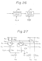
- FIG. 26 shows a block diagram of an embodiment of the flip-flop FF shown in Fig. 24.
- the flip-flop FF includes a master latch circuit ML driven, by a clock CLK and a slave latch circuit SL driven by an inverted clock CLK.
- FIG. 27 shows a specific circuit diagram of the flip-flop FF shown in Fig. 26.
- reference V S denotes a reference voltage supply
- CS4 to CS6 denote current sources. The operation will be briefly described.
- a transistor Q40 is turned ON, a transistor Q41 is turned OFF, a transistor Q46 is turned OFF and a transistor Q47 is turned ON, thus outputting a signal S5 having a low level and a signal S6 having a high level.
- a transistor Q43 is turned ON, a transistor Q44 is turned OFF, and a transistor Q45 is turned OFF.
- the flip-flop FF shown in Fig. 27 functions as a discrimination circuit which reads data in response to the levels of the input signals S3 and S4 at a change time of the clock CLK, with a narrow pulse width of the clock CLK.
- the discrimination threshold level L is shifted by a half (1/2) of the level shift of the signal S4. Also, the dead band of the discrimination shown in Fig. 21 is narrowed by a half.
- the signals S10A and S10B correspond to the input signals S IN1 and S IN2
- the circuit shown in Fig. 25 including the flip-flop FF corresponds to the signal discrimination circuit 12.
- the clock CLK in Fig. 27 is supplied from the timing circuit 14 shown in Fig. 19.
- the signal discrimination circuit of the present invention is formed by a combination of the level shift circuit, which is differential-operated and can shift the levels of the differential-input signals S IN1 and S IN2 , and a latch circuit, such as the flip-flop FF, latching the level-shifted output signals S OUT1 and S OUT2 .
- the signal discrimination circuit of the present invention can adjust the discrimination threshold level L and has a narrow dead band. The narrow dead band brings a reduction of an amplitude of the equalized signal, resulting in a prevention of cross-talk.
- the signal discrimination circuit of the present invention can operate at a high speed will improving the frequency characteristic and the wave form response characteristic.
- the signal discrimination circuit is preferably used for discriminating the OE converted signal because the free level shift is effective for discriminating a center eye-pattern lowered due to an optical shock.
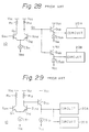
- Figure 28 shows a prior art signal distribution circuit.
- a signal sending circuit 10 is a differential-operation pair type circuit consisting of resistors R51 and R52 , transistors Q51 and Q52 and a constant current source CS51.
- Two parallel-connected emitter-follower circuits which consist of a transistor Q101 and a constant current source CS101 , and a transistor Q102 and a constant current source CS102 , respectively, are connected to a collector of the transistor Q52.
- Two circuits 20A and 20B, which receive distributed signals follow the emitter-follower circuits.
- Figure 29 also shows a prior art signal distribution circuit.
- a single emitter-follower circuit consisting of the transistor Q101 and the constant current source CS101 is provided to supply two distributed signals to the circuits 20A and 20B. Since the input impedance of the circuits 20A and 20B are connected to an output terminal of the emitter-follower transistor Q101 , the frequency characteristic often may be fluctuated. In addition, the mutual status change of the circuits 20A and 20B adversely affects the signal distribution circuit. Also, this signal distribution circuit does not provide sufficient fan-outs.
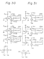
- Figures 30 and 31 are circuit diagrams showing the principle of a signal distribution circuit.
- the signal distribution circuit shown in Fig. 30 includes a current drive source ID having at least one transistor, an emitter of which is operatively grounded and a base of which receives an input signal S IN , and series-connected base-grounded transistor circuits, for example, a base-grounded transistor circuit composed of a base-grounded transistor Q21 and a resistor R21. An emitter of each base-grounded transistor circuit is operatively connected to a collector of the transistor in the current drive source ID. Accordingly, the above circuit configuration is formed as a cascode configuration.
- a bias current source BC is connected between each emitter of the base-grounded transistor, for example, Q27 and ground.
- a plurality of emitter-follower circuits each, for example, an emitter-follower circuit composed of an emitter-follower transistor Q101 and a current source CS101 , can be connected to collectors of the base-grounded transistors.
- the circuits 20A to 20G are also connected to the emitter-follower circuits.
- the signal distribution circuit shown in Fig. 30 changes the voltage input signal S IN to a current signal I passing through the series-connected base-grounded transistor circuits.
- Each voltage drop generated at each load resistor, for example, R21 is supplied to the base of a corresponding emitter-follower transistor, for example, Q101 , to distribute the input signal S IN .
- the frequency characteristic is not distorted and the adverse affect due to the circuits 20A to 20G is avoided.
- the load resistors are separated by the base-grounded transistors, and thus the frequency characteristic is not adversely affected by the stray capacitors.
- the bias current source BC the adverse affect due the stray capacitance superimposed on the voltage of the transfer lines l is fully eliminated.
- the signal distribution circuit shown in Fig. 30 operates at a high speed without a distortion of the frequency characteristic and the wave form response characteristic, and can provide many fan-outs regardless of the superimposition of the stray capacitance.
- the signal distribution circuit shown in Fig. 31 includes the current drive source ID, parallel-connected base-grounded transistor circuits, and the bias current source BC. Optionally, a plurality of emitter-follower circuits and the circuits 20A to 20C are provided. The operation of the signal distribution circuit is similar to that of the signal distribution circuit shown in Fig. 30. The features of the signal distribution circuit shown in Fig. 31 are also similar to those of the signal distribution circuit shown in Fig. 30.
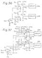
- Figures 32 to 37 show circuit diagrams of the signal distribution circuits shown in Figs. 30 and 31.
- the signal distribution circuits shown in Figs. 32 and 33 correspond to the signal distribution circuit shown in Fig. 30.
- the bases of base-grounded transistors Q21 , Q22 , Q 21a , Q 21b , Q 22a and Q 22b are grounded through bias voltage supply circuits V B1 and V B2 .
- Emitters of transistors Q31 , Q11 , and Q12 are grounded through a resistor R51 functioning as the current source and a current source CS11.
- the bias current source BC is formed by a resistor R41. Since the signal distribution circuit shown in Fig. 33 is differentially operated, two bias current sources BC a and BC b are provided.
- the signal distribution circuits shown in Figs. 36 to 37 correspond to the signal distribution circuit shown in Fig. 31.
- the bias current source BC is formed by a current-mirror type current source circuit.
- the signal distribution circuit shown in Fig. 37 is differentially operated.
- a signal synthesization circuit will be described.
- Figures 38 and 39 show prior art signal synthesization circuits. The operation of these signal synthesization circuits is well known, and thus a description thereof is omitted.
- emitter-follower outputs of transistors Q30 and Q40 are connected to a circuit 40.
- the signal synthesization circuit shown in Fig. 38 suffers from the same defects as those of the signal distribution shown in Fig. 29.
- the signal synthesization circuit shown in Fig. 39 suffers from defects similar to those of the signal distribution circuit shown in Fig. 28, since base-collector capacitors of transistors Q30 and Q40 are connected to a load resistor R in parallel.
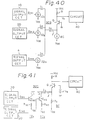
- Figure 40 shows a circuit diagram showing the principle of a signal synthesization circuit.
- the signal synthesization circuit includes a plurality current drive sources ID1 to ID n provided in correspondance to the number of input signals S IN1 to S INn to be synthesized, a base-grounded transistor Q, a load resistor R, and a bias current source BC.
- Each current drive source ID includes a transistor, an emitter thereof being operatively grounded, and a base thereof receiving the input signal S IN .
- the signal synthesization circuit is basically formed by a combination of the cascode configuration circuit and the current source BC.
- the synthesized current signal I0 is changed to a voltage V0 at the load resistor R. This voltage V0 is supplied to a circuit 40.
- the base-grounded transistor Q separates a connection between the current drive sources ID1 to ID n and the load resistor R, the adverse affect due to a stray capacitance on the current drive sources ID1 to ID n is prevented.
- output impedances of the current drive sources ID1 to ID n are high, a mutual interface between the current drive sources ID1 to ID n is substantially avoided.
- the provision of the bias current source BC eliminates the adverse affect due to the stray capacitor connected to the transfer line l.
- the signal synthesization circuit shown in Fig. 40 provide many fan-ins, and operates at a high speed without a distortion of the frequency characteristic.
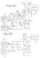
- Figures 41 and 42 show further signal synthesization circuits.
- Figure 43 shows circuit diagram of an embodiment of the signal synthesization circuit in accordance with present invention. The configuration and the operation of these signal synthesization circuits are apparent from the above description.
- a signal synthesization circuit of the present invention overcomes the above defects of the load resistor commonly used type signal synthesization circuit shown in Fig. 39.
Landscapes
- Engineering & Computer Science (AREA)
- Computer Hardware Design (AREA)
- Physics & Mathematics (AREA)
- Computing Systems (AREA)
- General Engineering & Computer Science (AREA)
- Mathematical Physics (AREA)
- Power Engineering (AREA)
- Nonlinear Science (AREA)
- Amplifiers (AREA)
- Logic Circuits (AREA)
Abstract
Claims (10)
- Circuit de décalage de niveau comprenant :
un circuit de commande de courant (ID) incluant au moins un transistor d'entrée (Q₁₁, Q₁₂; Q₃₀, Q₄₀), son émetteur étant mis à la masse en fonctionnement et sa base recevant un signal d'entrée respectif (SIN1; SIN2) ;
un circuit de transistor de charge incluant au moins un transistor de charge (Q ; Q₂₁ ; Q₂₂), la base de chaque transistor de charge étant mise à la masse en fonctionnement, I'émetteur de chaque transistor de charge étant connecté au collecteur d'un transistor d'entrée respectif (Q₁₁, Q₁₂ ; Q₃₀, Q₄₀) ;
une source de courant de polarisation connectée entre ledit émetteur dudit transistor de charge et une masse, un courant respectif généré par ladite source de courant de polarisation étant appliqué à chaque transistor de charge pour maintenir une tension base-émetteur en sens direct (VBE) de chaque transistor de charge ; et
un circuit de résistance de charge incluant au moins une résistance de charge (R ; R₂₁, R₂₂) connectée entre le collecteur d'un transistor de charge respectif (Q ; Q₂₁, Q₂₂) dans ledit circuit de transistor de charge et une tension d'alimentation (VCC), un signal de sortie (SOUT1, SOUT2) étant prévu au niveau du collecteur de chaque transistor de charge,
caractérisé en ce que
ladite source de courant de polarisation comprend un circuit miroir de courant (CS₂, CS₃) pour chaque courant devant être généré, au moins l'un desdits circuits miroirs de courant étant connecté à une source de tension de commande (Vc) pour décaler le niveau dudit signal de sortie d'une valeur définie par la source de tension de commande (Vc). - Circuit de décalage de niveau selon la revendication 1, caractérisé en ce que ledit circuit de commande de courant (ID) inclut des premier et second transistors d'entrée (Q₁₁ et Q₁₂) connectés en parallèle de manière à fonctionner de façon différentielle en réponse à deux signaux d'entrée (SIN1 et SIN2) connectés à leurs bases et une source de courant (CS₁) connectée entre des émetteurs desdits premier et second transistors (Q₁₁, Q₁₂) et la masse ;
ledit circuit de transistor de charge inclut des premier et second transistors de charge (Q₂₁ et Q₂₂), l'émetteur dudit premier transistor de charge étant connecté au collecteur dudit premier transistor d'entrée, I'émetteur dudit second transistor de charge étant connecté au collecteur dudit second transistor d'entrée et les bases desdits premier et second transistors de charge étant connectées en commun et mises à la masse en fonctionnement,
ledit circuit de résistance de charge inclut :
deux résistances de charge (R₂₁ et R₂₂) respectivement connectées aux collecteurs desdits premier et second transistors de charge, afin de générer en sortie deux signaux de sortie (SOUT1 et SOUT2) à partir de points au niveau desquels lesdits collecteurs et lesdites résistances de charge sont connectés en commun ; et
ledit circuit miroir de courant inclut des premier à troisième transistors de source de courant (Q₄ ; Q₅ et Q₁₄ ; Q₈, Q₉ et Q₁₃) connectés en parallèle, les collecteurs desdits premier et second transistors de source de courant (Q₄, Q₅ ; Q₈, Q₉) étant respectivement connectés auxdits émetteurs desdits premier et second transistors de charge, la source de tension de commande (VC) étant connectée à un collecteur dudit troisième transistor de source de courant (Q₁₄), le collecteur dudit troisième transistor de source de courant (Q₁₄ ; Q₁₃) étant connecté à sa base qui est connectée en commun à la base dudit second transistor de source de courant (Q₅ ; Q₉) et des seconde à quatrième résistances de source de courant (R₄, R₅ et R₁₂ ; R₄, R₅ et R₁₀) respectivement connectées entre les émetteurs desdits premier à troisième transistors de source de courant et la masse. - Circuit de décalage de niveau selon la revendication 1, caractérisé en ce que ledit circuit de commande de courant (ID) inclut des premier et second transistors d'entrée (Q₁₁ et Q₁₂) connectés en parallèle de manière à fonctionner de façon différentielle en réponse à deux signaux d'entrée (SIN1 et SIN2) connectés à leurs bases et une source de courant (CS₁) connectée entre les émetteurs desdits premier et second transistors d'entrée et la masse,
ledit circuit de transistor de charge inclut des premier et second transistors de charge (Q₂₁ et Q₂₂), l'émetteur dudit premier transistor de charge étant connecté au collecteur dudit premier transistor d'entrée, I'émetteur dudit second transistor de charge étant connecté au collecteur dudit second transistor d'entrée et les bases desdits premier et second transistors de charge étant connectées en commun et mises à la masse en fonctionnement,
ladite résistance de charge inclut :
deux résistances de charge (R₂₁ et R₂₂) respectivement connectées aux collecteurs desdits premier et second transistors de charge, afin de générer en sortie deux signaux de sortie (SOUT1 et SOUT2) à partir de points au niveau desquels lesdits collecteurs et lesdites résistances de charge sont connectés en commun ; et
ledit circuit miroir de courant inclut des premier à troisième transistors de source de courant (Q₄, Q₅ et Q₁₄) connectés en parallèle, les collecteurs desdits premier et second transistors de source de courant (Q₄, Q₅) étant respectivement connectés auxdits émetteurs desdits premier et second transistors de charge, la source de tension de commande (VC) étant connectée à un collecteur dudit troisième transistor de source de courant (Q₁₄), le collecteur dudit troisième transistor de source de courant étant connecté à sa base qui est connectée en commun aux bases desdits premier et second transistors de source de courant, et desdites seconde à quatrième résistances de source de courant (R₄, R₅ et R₁₂) sont respectivement connectées entre les émetteurs desdits premier à troisième transistors de source de courant et la masse. - Circuit de décalage de niveau selon la revendication 2, caractérisé en ce qu'un circuit de bascule (FF) est connecté par ses entrées audit circuit de résistance de charge.
- Circuit de décalage de niveau selon la revendication 1, caractérisé en ce que :
ledit circuit de commande de courant (ID) inclut des premier et second transistors d'entrée (Q₁₁ et Q₁₂) connectés en parallèle de manière à fonctionner de façon différentielle en réponse à deux signaux d'entrée (SIN1 et SIN2) connectés à leurs bases et une source de courant (CS₁) connectée entre les émetteurs desdits premier et second transistors d'entrée (Q₁₁, Q₁₂) et la masse,
ledit circuit de transistor de charge inclut des premier et second transistors de charge (Q₂₁ et Q₂₂), l'émetteur dudit premier transistor de charge étant connecté au collecteur dudit premier transistor d'entrée, I'émetteur dudit second transistor de charge étant connecté au collecteur dudit second transistor d'entrée et les bases desdits premier et second transistors de charge étant connectées en commun et mises à la masse en fonctionnement,
ledit circuit de résistance de charge inclut :
deux résistances de charge (R₂₁ et R₂₂) respectivement connectées aux collecteurs desdits premier et second transistors de charge, afin de générer en sortie deux signaux de sortie (SOUT1 et SOUT2) à partir de points au niveau desquels lesdits collecteurs et lesdites résistances de charge sont connectés en commun, et
ladite source de courant de polarisation inclut :
les premier et second circuits miroirs de courant (CS₂, CS₃) connectés auxdits premier et second transistors de charge. - Circuit de décalage de niveau selon la revendication 5, caractérisé en ce que ledit premier circuit miroir de courant est connecté à la source de tension de commande (VC) pour modifier un courant généré par celle-ci.
- Circuit de décalage de niveau selon la revendication 5, caractérisé en ce que ledit second circuit miroir de courant est connecté à la source de tension de commande (VC) pour modifier un courant généré par celle-ci.
- Circuit de décalage de niveau selon la revendication 1, caractérisé en ce qu'une pluralité desdits circuits de commande de courant (ID₁ à IDn) sont connectés en parallèle, chaque circuit de commande de courant se voyant appliquer un dit signal d'entrée (SIN) devant être synthétisé, ladite source de courant de polarisation et ledit émetteur dudit au moins un transistor de charge (Q) dans ledit circuit de transistor de charge sont connectés aux collecteurs connectés en commun desdits circuits de commande de courant parallèles.
- Circuit de décalage de niveau selon la revendication 4, caractérisé en ce que ledit circuit de bascule (FF) inclut un circuit de bascule maître (ML) commandé par un signal d'horloge (CLK) et un circuit de bascule esclave (SL) commandé par un signal d'horloge inversé (CLK).
- Circuit de décalage de niveau selon la revendication 9, caractérisé en ce que ledit circuit de bascule maître (ML) comprend :
une première paire de transistors en suiveurs d'émetteur (Q₄₀, Q₄₁) connectés en parallèle, leurs bases étant connectées audit circuit de résistance de charge, leurs collecteurs étant connectés à une tension d'alimentation (Vcc) via des résistances de charge respectives (R₄₁, R₄₂) et leurs émetteurs étant connectés à un transistor (Q₄₂) qui se voit appliquer ledit signal d'horloge (CLK) au niveau de sa base ; et
une seconde paire de transistors en suiveurs d'émetteur (Q₄₃, Q₄₄) connectés en parallèle, leurs bases étant connectées aux collecteurs respectifs de la première paire de transistors en suiveurs d'émetteur (Q₄₀, Q₄₁) et leurs émetteurs étant connectés à un transistor (Q₄₅) qui reçoit une tension de référence (VS) au niveau de sa base ;
dans lequel les émetteurs desdits transistors (Q₄₂, Q₄₅) sont connectés à une source de courant constant (CS₄).
Applications Claiming Priority (13)
| Application Number | Priority Date | Filing Date | Title |
|---|---|---|---|
| JP18984987 | 1987-07-29 | ||
| JP189849/87 | 1987-07-29 | ||
| JP18984887 | 1987-07-29 | ||
| JP189848/87 | 1987-07-29 | ||
| JP189851/87 | 1987-07-29 | ||
| JP18985087 | 1987-07-29 | ||
| JP189850/87 | 1987-07-29 | ||
| JP18985187 | 1987-07-29 | ||
| JP191040/87 | 1987-07-30 | ||
| JP19104087 | 1987-07-30 | ||
| JP231818/87 | 1987-09-16 | ||
| JP23181887 | 1987-09-16 | ||
| PCT/JP1988/000758 WO1989001262A2 (fr) | 1987-07-29 | 1988-07-28 | Circuit electronique a haute vitesse presentant une configuration cascode |
Publications (2)
| Publication Number | Publication Date |
|---|---|
| EP0329793A1 EP0329793A1 (fr) | 1989-08-30 |
| EP0329793B1 true EP0329793B1 (fr) | 1995-10-25 |
Family
ID=27553625
Family Applications (1)
| Application Number | Title | Priority Date | Filing Date |
|---|---|---|---|
| EP88906881A Expired - Lifetime EP0329793B1 (fr) | 1987-07-29 | 1988-07-28 | Circuit electronique a haute vitesse presentant une configuration cascode |
Country Status (4)
| Country | Link |
|---|---|
| EP (1) | EP0329793B1 (fr) |
| CA (1) | CA1301267C (fr) |
| DE (1) | DE3854617T2 (fr) |
| WO (1) | WO1989001262A2 (fr) |
Families Citing this family (8)
| Publication number | Priority date | Publication date | Assignee | Title |
|---|---|---|---|---|
| JP2583570B2 (ja) * | 1988-05-02 | 1997-02-19 | 株式会社東芝 | インターフェイス回路 |
| JPH0345045A (ja) * | 1989-07-13 | 1991-02-26 | Fujitsu Ltd | 信号入出力インタフェース回路 |
| DE4290570T1 (fr) * | 1991-03-04 | 1993-04-01 | Motorola, Inc., Schaumburg, Ill., Us | |
| US5939922A (en) * | 1995-09-13 | 1999-08-17 | Kabushiki Kaisha Toshiba | Input circuit device with low power consumption |
| JP3391374B2 (ja) | 1998-12-25 | 2003-03-31 | 富士通株式会社 | クロスポイントスイッチ回路および基本スイッチセル電子回路 |
| DE10317213A1 (de) * | 2003-04-15 | 2004-11-04 | Robert Bosch Gmbh | Pegelwandler |
| US8283946B2 (en) | 2010-04-15 | 2012-10-09 | Micron Technology, Inc. | Signaling systems, preamplifiers, memory devices and methods |
| DE102021103807A1 (de) | 2021-02-18 | 2022-08-18 | Endress+Hauser SE+Co. KG | Pegelwandler |
Family Cites Families (14)
| Publication number | Priority date | Publication date | Assignee | Title |
|---|---|---|---|---|
| GB909776A (en) * | 1960-08-30 | 1962-11-07 | Nippon Electric Co | A transistor amplifier with gain control |
| NL282779A (fr) * | 1961-09-08 | |||
| US3200343A (en) * | 1961-12-29 | 1965-08-10 | Leeds & Northrup Co | D.c. amplifier having fast recovery characteristics |
| US3496385A (en) * | 1966-02-28 | 1970-02-17 | Xerox Corp | High voltage compensated transistorized switching apparatus |
| US3516003A (en) * | 1968-07-30 | 1970-06-02 | Bailey Meter Co | High-gain single-stage a.c. cascode amplifier circuit |
| JPS5297046U (fr) * | 1976-01-19 | 1977-07-20 | ||
| CA1134463A (fr) * | 1978-10-13 | 1982-10-26 | Kyoichi Murakami | Circuit de conversion de signaux a la masse en paires de signaux differentiels |
| US4340866A (en) * | 1979-09-17 | 1982-07-20 | Tektronix, Inc. | Thermally-compensated variable gain differential amplifier |
| JPS5843836B2 (ja) * | 1979-12-21 | 1983-09-29 | 富士通株式会社 | デコ−ダ回路 |
| DE3217237A1 (de) * | 1982-05-07 | 1983-11-10 | Siemens AG, 1000 Berlin und 8000 München | Schaltungsanordnung zur pegelumsetzung |
| US4528517A (en) * | 1983-02-07 | 1985-07-09 | Tektronix, Inc. | Overdrive thermal distortion compensation for a Quinn cascomp amplifier |
| JPS6090407A (ja) * | 1983-10-24 | 1985-05-21 | Toshiba Corp | 差動増幅器 |
| DE3484101D1 (de) * | 1984-01-05 | 1991-03-14 | Ant Nachrichtentech | Breitbandkoppelfeld in matrixform. |
| FR2592538B1 (fr) * | 1985-12-31 | 1988-02-12 | Radiotechnique Compelec | Etage amplificateur differentiel pour hautes frequences et amplificateur le comportant. |
-
1988
- 1988-07-28 WO PCT/JP1988/000758 patent/WO1989001262A2/fr not_active Ceased
- 1988-07-28 EP EP88906881A patent/EP0329793B1/fr not_active Expired - Lifetime
- 1988-07-28 DE DE3854617T patent/DE3854617T2/de not_active Expired - Fee Related
- 1988-07-29 CA CA000573461A patent/CA1301267C/fr not_active Expired - Lifetime
Non-Patent Citations (2)
| Title |
|---|
| "How it works", page 13 * |
| pages 1173-1175 * |
Also Published As
| Publication number | Publication date |
|---|---|
| DE3854617T2 (de) | 1996-03-28 |
| WO1989001262A3 (fr) | 1989-02-23 |
| CA1301267C (fr) | 1992-05-19 |
| WO1989001262A2 (fr) | 1989-02-09 |
| DE3854617D1 (de) | 1995-11-30 |
| EP0329793A1 (fr) | 1989-08-30 |
Similar Documents
| Publication | Publication Date | Title |
|---|---|---|
| JP3576702B2 (ja) | 可変ハイパスフィルタ | |
| KR970000063B1 (ko) | 버스트 모드 디지탈 데이타 수신기 | |
| US5124592A (en) | Active filter | |
| US5844445A (en) | Feedback type pre-amplifier | |
| US5343160A (en) | Fully balanced transimpedance amplifier with low noise and wide bandwidth | |
| EP0315376B1 (fr) | Elément de retard ajustable pour systèmes numériques | |
| EP0600852B1 (fr) | Arrangements pour circuit logique | |
| US5510745A (en) | High-speed electronic circuit having a cascode configuration | |
| US5900779A (en) | Differential transimpedance amplifier | |
| EP0302548A2 (fr) | Circuit pour générer une onde de courant de forme trapézoidale avec des temps de montée et de descente assortis | |
| US4701720A (en) | Capacitive feedback to boost amplifier slew rate | |
| HK15393A (en) | Bridge amplifier | |
| KR19990067387A (ko) | 범용 수신장치 | |
| US5418492A (en) | Fully differential non-op-amp-based positive feedback BJT biquad filter | |
| US10999055B2 (en) | SerDes systems and differential comparators | |
| US6268769B1 (en) | Operational amplifier | |
| US5003269A (en) | Unity gain amplifier with high slew rate and high bandwidth | |
| JP3470797B2 (ja) | バッファ回路 | |
| JPH09186659A (ja) | 増幅回路 | |
| KR100381410B1 (ko) | 다단 궤환형 버스트모드 광수신기 | |
| WO1989001262A2 (fr) | Circuit electronique a haute vitesse presentant une configuration cascode | |
| US6538790B1 (en) | Optical receiver array | |
| US6529036B1 (en) | Low noise, reduced swing differential output buffer design | |
| JPH02500238A (ja) | カスコード構成の高速電子回路 | |
| JP3062225B2 (ja) | 信号伝送方法及び回路 |
Legal Events
| Date | Code | Title | Description |
|---|---|---|---|
| PUAI | Public reference made under article 153(3) epc to a published international application that has entered the european phase |
Free format text: ORIGINAL CODE: 0009012 |
|
| 17P | Request for examination filed |
Effective date: 19890329 |
|
| AK | Designated contracting states |
Kind code of ref document: A1 Designated state(s): DE FR GB |
|
| 17Q | First examination report despatched |
Effective date: 19900807 |
|
| GRAA | (expected) grant |
Free format text: ORIGINAL CODE: 0009210 |
|
| AK | Designated contracting states |
Kind code of ref document: B1 Designated state(s): DE FR GB |
|
| REF | Corresponds to: |
Ref document number: 3854617 Country of ref document: DE Date of ref document: 19951130 |
|
| ET | Fr: translation filed | ||
| PLBE | No opposition filed within time limit |
Free format text: ORIGINAL CODE: 0009261 |
|
| STAA | Information on the status of an ep patent application or granted ep patent |
Free format text: STATUS: NO OPPOSITION FILED WITHIN TIME LIMIT |
|
| 26N | No opposition filed | ||
| REG | Reference to a national code |
Ref country code: GB Ref legal event code: IF02 |
|
| PGFP | Annual fee paid to national office [announced via postgrant information from national office to epo] |
Ref country code: FR Payment date: 20030711 Year of fee payment: 16 |
|
| PGFP | Annual fee paid to national office [announced via postgrant information from national office to epo] |
Ref country code: GB Payment date: 20030723 Year of fee payment: 16 |
|
| PGFP | Annual fee paid to national office [announced via postgrant information from national office to epo] |
Ref country code: DE Payment date: 20030807 Year of fee payment: 16 |
|
| PG25 | Lapsed in a contracting state [announced via postgrant information from national office to epo] |
Ref country code: GB Free format text: LAPSE BECAUSE OF NON-PAYMENT OF DUE FEES Effective date: 20040728 |
|
| PG25 | Lapsed in a contracting state [announced via postgrant information from national office to epo] |
Ref country code: DE Free format text: LAPSE BECAUSE OF NON-PAYMENT OF DUE FEES Effective date: 20050201 |
|
| GBPC | Gb: european patent ceased through non-payment of renewal fee |
Effective date: 20040728 |
|
| PG25 | Lapsed in a contracting state [announced via postgrant information from national office to epo] |
Ref country code: FR Free format text: LAPSE BECAUSE OF NON-PAYMENT OF DUE FEES Effective date: 20050331 |
|
| REG | Reference to a national code |
Ref country code: FR Ref legal event code: ST |