EP0330724A2 - Commutateur électronique de courant élevé pour un circuit à alimentation unique - Google Patents
Commutateur électronique de courant élevé pour un circuit à alimentation unique Download PDFInfo
- Publication number
- EP0330724A2 EP0330724A2 EP88109548A EP88109548A EP0330724A2 EP 0330724 A2 EP0330724 A2 EP 0330724A2 EP 88109548 A EP88109548 A EP 88109548A EP 88109548 A EP88109548 A EP 88109548A EP 0330724 A2 EP0330724 A2 EP 0330724A2
- Authority
- EP
- European Patent Office
- Prior art keywords
- switching transistor
- transistor
- converter
- circuit
- large current
- Prior art date
- Legal status (The legal status is an assumption and is not a legal conclusion. Google has not performed a legal analysis and makes no representation as to the accuracy of the status listed.)
- Ceased
Links
Images
Classifications
-
- H—ELECTRICITY
- H03—ELECTRONIC CIRCUITRY
- H03K—PULSE TECHNIQUE
- H03K17/00—Electronic switching or gating, i.e. not by contact-making and –breaking
- H03K17/51—Electronic switching or gating, i.e. not by contact-making and –breaking characterised by the components used
- H03K17/56—Electronic switching or gating, i.e. not by contact-making and –breaking characterised by the components used by the use, as active elements, of semiconductor devices
- H03K17/60—Electronic switching or gating, i.e. not by contact-making and –breaking characterised by the components used by the use, as active elements, of semiconductor devices the devices being bipolar transistors
- H03K17/601—Electronic switching or gating, i.e. not by contact-making and –breaking characterised by the components used by the use, as active elements, of semiconductor devices the devices being bipolar transistors using transformer coupling
-
- H—ELECTRICITY
- H03—ELECTRONIC CIRCUITRY
- H03K—PULSE TECHNIQUE
- H03K17/00—Electronic switching or gating, i.e. not by contact-making and –breaking
- H03K17/08—Modifications for protecting switching circuit against overcurrent or overvoltage
- H03K17/081—Modifications for protecting switching circuit against overcurrent or overvoltage without feedback from the output circuit to the control circuit
- H03K17/0812—Modifications for protecting switching circuit against overcurrent or overvoltage without feedback from the output circuit to the control circuit by measures taken in the control circuit
- H03K17/08126—Modifications for protecting switching circuit against overcurrent or overvoltage without feedback from the output circuit to the control circuit by measures taken in the control circuit in bipolar transitor switches
-
- H—ELECTRICITY
- H03—ELECTRONIC CIRCUITRY
- H03K—PULSE TECHNIQUE
- H03K2217/00—Indexing scheme related to electronic switching or gating, i.e. not by contact-making or -breaking covered by H03K17/00
- H03K2217/0036—Means reducing energy consumption
Definitions
- the present invention relates to an electronic large current switch for a single power circuit, and more particularly to an electronic switch applicable to a vehicle having a single DC power supply.
- the conventional switches typically used to control the power supply to electrical loads of a vehicle, such as lamps, window wipers, etc., are classified into mechanical relay switches and electronic switches.
- the conventional relay switch has the disadvantages that the state of the contacts for the relay may be unstable and malfunctions of the contacts may occur due to external vibration or impact. Also, the state of the contacts deteriorates when foreign matter such as dust comes in contact with the contacts or when the contacts are partly corroded. Furthermore, when switching a large current load by such relay contacts, the contacts are apt to stick to each other or harm adjacent electronic instruments due to electric arcs which occur between the contacts.
- the conventional electronic switch which uses a transistor as a switching element thereof is generally designed to switch a relatively small current load of approximately 2 to 3 amperes and thus the saturation voltage between the collector and the emitter of the switching transistor becomes a high level of 1 to 2 volts because the base current thereof is several tens to several hundreds of milliamperes in accordance with electrical characteristics such as the parameters or the operating condition of the switching transistor.
- this type of electronic switch is used as a controller of the power supply for a vehicle, however, the switching transistor controls a large current load of 10 to 15 amperes supplied to the electrical loads.
- the power consumption by the switching transistor becomes relatively high and, accordingly, the switching transistor deteriorates quickly due to heat generation within the transistor.
- a method for reducing the power consumption of the switching transistor may be considered.
- the method is to design a switching circuit with a lower saturation voltage by increasing the base current of the switching transistor.
- the power consumption by the resistor is very high because of a large current load through the resistor and the high voltage difference across the resistor. Therefore, as the power consumption capacity of the resistor must be set high, the size of the resistor increases which in turn makes it difficult to manufacture the electronic switch small, and it can not be the solution to the problem of power loss.
- the method of setting the bias voltage by connecting the bleeder type bias resistor to the switching transistor of a Darlington connection may also be considered, but the heat generation of the switching transistor which controls a large current load can not be reduced and the parameters of the transistor are changed due to the generated heat. Therefore, the use of a heat sink having a large surface area is inevitable to radiate the high heat generated within the switching transistor. However, the use of a heat sink alone is not so effective in handling the heat continuously generated in the transistor and accordingly, the switching transistor may not perform effectively and it is difficult to make the product small.
- the conventional electronic switch comprising the transistor as the switching element and the bias circuit is used as the controller of the power supply for a vehicle having a single power supply, the heat loss within the transistor increases and it is difficult to make the product small.
- an electronic switch having a DC-to-DC converter by which the input voltage from a power source is lowered and a switching transistor which is driven by the lowered voltage and controls the power supply to the electrical loads of a vehicle.
- the low voltage output from the DC-to-DC converter is supplied to the base of the switching transistor with increased base current of approximately 1 ampere and thus the saturation voltage of the transistor can be set at the level of 0.2 to 0.4 volts.
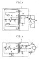
- rectifying diodes D2 and D3 and a smoothing condenser C1 are connected to the secondary coil L2 of a transformer T1 in a Royer's DC-to-DC converter 1, which transforms the voltage of a battery BT for the vehicle to a low level.
- the low voltage output from this DC-to-DC converter 1 is then applied to the base of the switching transistor TR3.
- the electrical load circuit 2 and the battery BT are connected in series.
- the electrical load circuit 2 may be composed of various vehicle lamps such as headlights, turn indicators, brake lights and a window wiper driving motor.
- the DC-to-DC converter 1 in the preferred embodiments is an oscillator employing the magnetic saturation of the core, i. e., employing the magnetization characteristic of the core in the transformer T1, wherein the magnetic flux density at first increases according to the increase of the magnetic field intensity but does not change further beyond the saturation point thereof.
- the control switch SW1 connected to the primary coil L1 of the transformer T1 in the DC-to-DC converter 1 is turned on, the 12 VDC power supply from the battery BT is applied to the primary coil L1 and accordingly, the driving current is applied to each base of transistors TR1 and TR2 through the resistor R1 and the other primary coils La and La′ respectively.
- one of the transistors TR1 and TR2 is turned on first depending on the characteristics of the parameters of the transistors. For example, if the transistor TR1 is turned on first, the collector current thereof flows through the coil L1 and thus the transistor TR1 can be saturated accroding to the increase of the base current of the transistor TR1 which is due to the increase of the voltage induced in the coil La by the coil L1. Therefore, with the increase of the current through the coil L1, the magnetic flux density of the core reaches the saturation point where there is no change of the magnetic field and thus no further voltage is induced in the coil La as described above resulting in that the transistor TR1 is turned off. After the transistor TR1 is turned off, the transistor TR2 becomes turned on and the same circuit operation is repeated as mentioned above.
- the voltage induced in this way becomes a full waved rectified voltage through the diodes D2 and D3, smoothed through the condenser C1 and then applied to the switching transistor TR3 as the base bias voltage thereof.
- the switching transistor TR3 is turned on and the power supply is connected to the load circuit 2 through the transistor TR3.
- the saturation voltage of the switching transistor TR3 can be lowered about 0.3 vlots by increasing its base current to the level of about 1 ampere and accordingly, it is possible to minimize the power loss in the switching transistor TR3.
- the heat generation in the switching transistor TR3 is also minimized and neither the heat sink for heat radiation nor the bias resistor having a high power consumption capacity is necessary.
- the control switch SW1 in the DC-to-DC converter 1 is turned off, the power supply to each of the primary coils L1, La and La′ of the transformer T1 is cut out and then both transistors TR1 and TR2 are turned off. Therefore, the DC-to-DC converter 1 stops its operation and the base bias voltage applied to the switching transistor TR3 is cut off and thus the switching transistor T3 is turned off, causing the power supply from the battery BT to the load circuit 2 to be cut off.
- switching circuits can be employed according to the characteristics of the electrical load circuit 2 instead of the control switch SW1 in the DC-to-DC converter 1.
- a periodic switching circuit such as control circuits of the turn indicators and the wiper driving motor could be employed.
- FIG. 2 there is shown another embodiment of the present invention.
- Each element having the same function as a part in FIG. 1 has the same reference number with an apostrophe.
- a ringing chock converter 1′ is used instead of the Royer's DC-to-DC converter, and magnetic saturation characteristics are also employed.
- the control switch SW1′ is turned on, the driving current from the battery BT′ is applied to the base of a transistor TR4 through the primary coil L1′ of the transformer T1′, a resistor R2 and a condenser C2 connected in parallel.
- the transistor TR4 is turned on, and the collector current of the transistor TR4 flows through the primary coil L1′ of the transformer T1′.
- the voltage induced in the coil L1′ increases and thus the base current of the transistor TR4 also increases resulting in that the magnetic flux density reaches the saturation point when the transistor TR4 is turned off as described above.
- the voltage charged in the condenser C2 is then discharged through the resistor R2.
- the transistor TR4 becomes turned-on, and thus the above described operations are repeated. Consequently, the transistor TR4 acts as an oscillator by repeating ' turn on ' and ' turn off ' operations and accordingly, an AC voltage is induced in the secondary coil L2′ of the transformer T1′.
- the switching transistor TR3′ is turned on and the power supply from the battery BT′ is connected to the electrical load circuit 2′.
- any type of a DC-to-DC converter for low voltage transformation can be employed instead of the Royer's DC-to-DC converter and the ringing chock converter 1′ as described above.
- a field effect transistor may be employed as the switching transistor instead if the switching noise is a critical problem.
- the present invention provides a novel electronic large current switch specially designed to minimize the power loss of the switching transistor therein and to make the product small and integrated so that it is suitable for being adapted to a vehicle having a single power supply.
- An electronic large current switch for a single power circuit has a DC-to-DC converter for low vlotage transformation the operation of which is controlled by a control switch or a periodic switching circuit and a switching transistor supplied with the low voltage output of the DC-to-DC converter as its base bias voltage and which controls the power supply to an electrical load circuit so as to be capable of minimizing the power loss of the switching transistor and making the product small and integrated.
Landscapes
- Engineering & Computer Science (AREA)
- Power Engineering (AREA)
- Dc-Dc Converters (AREA)
- Electronic Switches (AREA)
Applications Claiming Priority (2)
| Application Number | Priority Date | Filing Date | Title |
|---|---|---|---|
| US07/162,751 US4887198A (en) | 1988-03-01 | 1988-03-01 | Electronic large current switch for a single power circuit |
| US162751 | 1998-09-29 |
Publications (2)
| Publication Number | Publication Date |
|---|---|
| EP0330724A2 true EP0330724A2 (fr) | 1989-09-06 |
| EP0330724A3 EP0330724A3 (fr) | 1990-08-08 |
Family
ID=22586991
Family Applications (1)
| Application Number | Title | Priority Date | Filing Date |
|---|---|---|---|
| EP88109548A Ceased EP0330724A3 (fr) | 1988-03-01 | 1988-06-15 | Commutateur électronique de courant élevé pour un circuit à alimentation unique |
Country Status (2)
| Country | Link |
|---|---|
| US (1) | US4887198A (fr) |
| EP (1) | EP0330724A3 (fr) |
Cited By (3)
| Publication number | Priority date | Publication date | Assignee | Title |
|---|---|---|---|---|
| WO1994017364A1 (fr) * | 1993-01-26 | 1994-08-04 | Honeywell Inc. | Alimentation electrique de transformateur simple pour giroscope a laser |
| RU2257007C1 (ru) * | 2004-02-09 | 2005-07-20 | Федеральное государственное унитарное предприятие "Научно-производственное предприятие "Алмаз" | Электронный ключ с трансформаторной развязкой |
| RU2360358C1 (ru) * | 2008-07-03 | 2009-06-27 | Открытое акционерное общество "Специальное конструкторско-технологическое бюро по релейной технике" (ОАО "СКТБ РТ") | Электронное реле с трансформаторной развязкой и с защитой от перегрузки по току |
Families Citing this family (3)
| Publication number | Priority date | Publication date | Assignee | Title |
|---|---|---|---|---|
| JPH06335247A (ja) * | 1993-05-20 | 1994-12-02 | Canon Inc | 電源装置 |
| US5444610A (en) * | 1993-10-22 | 1995-08-22 | Diversified Technologies, Inc. | High-power modulator |
| US6043636A (en) * | 1997-10-20 | 2000-03-28 | Diversified Technologies, Inc. | Voltage transient suppression |
Family Cites Families (3)
| Publication number | Priority date | Publication date | Assignee | Title |
|---|---|---|---|---|
| US3012181A (en) * | 1958-12-29 | 1961-12-05 | Gen Electric | Transistor low drain converter |
| US3858057A (en) * | 1973-11-28 | 1974-12-31 | Gte Automatic Electric Lab Inc | Solid state relay |
| DE2644507C3 (de) * | 1976-10-01 | 1984-07-26 | Siemens AG, 1000 Berlin und 8000 München | Verfahren zur Aussteuerung eines im Sättigungszustand betriebenen Transistors und Vorrichtung zur Durchführung des Verfahrens |
-
1988
- 1988-03-01 US US07/162,751 patent/US4887198A/en not_active Expired - Fee Related
- 1988-06-15 EP EP88109548A patent/EP0330724A3/fr not_active Ceased
Cited By (3)
| Publication number | Priority date | Publication date | Assignee | Title |
|---|---|---|---|---|
| WO1994017364A1 (fr) * | 1993-01-26 | 1994-08-04 | Honeywell Inc. | Alimentation electrique de transformateur simple pour giroscope a laser |
| RU2257007C1 (ru) * | 2004-02-09 | 2005-07-20 | Федеральное государственное унитарное предприятие "Научно-производственное предприятие "Алмаз" | Электронный ключ с трансформаторной развязкой |
| RU2360358C1 (ru) * | 2008-07-03 | 2009-06-27 | Открытое акционерное общество "Специальное конструкторско-технологическое бюро по релейной технике" (ОАО "СКТБ РТ") | Электронное реле с трансформаторной развязкой и с защитой от перегрузки по току |
Also Published As
| Publication number | Publication date |
|---|---|
| EP0330724A3 (fr) | 1990-08-08 |
| US4887198A (en) | 1989-12-12 |
Similar Documents
| Publication | Publication Date | Title |
|---|---|---|
| EP0124735B1 (fr) | Circuit de mise en oeuvre pour lampe à décharge | |
| EP0330724A2 (fr) | Commutateur électronique de courant élevé pour un circuit à alimentation unique | |
| WO1986001364A1 (fr) | Inverseur sensible a la charge pour lampe electroluminescente | |
| EP0883231B1 (fr) | Appareil d'alimentation de puissance | |
| US6236552B1 (en) | Relay drive circuit | |
| EP0519555A1 (fr) | Convertisseur de retour alimenté en courant avec interrupteur unique quasi push-pull | |
| KR101123907B1 (ko) | 전원 유닛을 가지는 회로 장치 | |
| JP3493840B2 (ja) | 電源装置 | |
| JP4030349B2 (ja) | 電源回路 | |
| KR900000981Y1 (ko) | 단일전원 회로용 전자식 대전류 스위치 | |
| US4928037A (en) | Protected discharge lamp lighting system | |
| JP3148145B2 (ja) | スイッチング電源 | |
| KR20000015607A (ko) | 모니터의 과전압 보호 회로 | |
| JP4286084B2 (ja) | 直流電源装置 | |
| KR0134332Y1 (ko) | 강압형 스위칭 레귤레이터 | |
| JP3694146B2 (ja) | 放電灯点灯装置 | |
| JPH01238468A (ja) | インバータ装置 | |
| JP2916927B2 (ja) | 発振回路のサージ電圧吸収回路 | |
| KR900001905Y1 (ko) | 리모콘 사용기기의 전원릴레이 구동회로 | |
| KR20000007851A (ko) | 양전원을 갖는 스위칭모드 전원공급장치 | |
| JP2006244878A (ja) | 車両用灯具の点灯制御装置 | |
| JP3888376B2 (ja) | 放電灯点灯装置 | |
| KR910007048Y1 (ko) | 주스위칭 트랜지스터의 베이스 드라이버회로 | |
| SU1720152A1 (ru) | Транзисторный ключ | |
| KR20000028435A (ko) | 스위칭 전원회로의 기동저항 스위칭회로 |
Legal Events
| Date | Code | Title | Description |
|---|---|---|---|
| PUAI | Public reference made under article 153(3) epc to a published international application that has entered the european phase |
Free format text: ORIGINAL CODE: 0009012 |
|
| AK | Designated contracting states |
Kind code of ref document: A2 Designated state(s): DE FR GB IT SE |
|
| RAP1 | Party data changed (applicant data changed or rights of an application transferred) |
Owner name: LEE, JANG BUM |
|
| RIN1 | Information on inventor provided before grant (corrected) |
Inventor name: LEE, YOUN SUN |
|
| PUAL | Search report despatched |
Free format text: ORIGINAL CODE: 0009013 |
|
| AK | Designated contracting states |
Kind code of ref document: A3 Designated state(s): DE FR GB IT SE |
|
| 17P | Request for examination filed |
Effective date: 19910116 |
|
| 17Q | First examination report despatched |
Effective date: 19921016 |
|
| STAA | Information on the status of an ep patent application or granted ep patent |
Free format text: STATUS: THE APPLICATION HAS BEEN REFUSED |
|
| 18R | Application refused |
Effective date: 19930321 |