EP0331233B1 - Verfahren zum Herstellen eines optischen Verbundelements und das auf diese Weise erhaltene Element - Google Patents
Verfahren zum Herstellen eines optischen Verbundelements und das auf diese Weise erhaltene Element Download PDFInfo
- Publication number
- EP0331233B1 EP0331233B1 EP89200427A EP89200427A EP0331233B1 EP 0331233 B1 EP0331233 B1 EP 0331233B1 EP 89200427 A EP89200427 A EP 89200427A EP 89200427 A EP89200427 A EP 89200427A EP 0331233 B1 EP0331233 B1 EP 0331233B1
- Authority
- EP
- European Patent Office
- Prior art keywords
- monomer
- layer
- liquid
- crystalline
- orientation
- Prior art date
- Legal status (The legal status is an assumption and is not a legal conclusion. Google has not performed a legal analysis and makes no representation as to the accuracy of the status listed.)
- Expired - Lifetime
Links
- 230000003287 optical effect Effects 0.000 title claims description 27
- 238000004519 manufacturing process Methods 0.000 title claims description 13
- 239000000178 monomer Substances 0.000 claims description 73
- 150000001875 compounds Chemical class 0.000 claims description 34
- 239000000758 substrate Substances 0.000 claims description 26
- 238000000034 method Methods 0.000 claims description 22
- 238000006116 polymerization reaction Methods 0.000 claims description 16
- 239000011248 coating agent Substances 0.000 claims description 11
- 238000000576 coating method Methods 0.000 claims description 11
- 239000003999 initiator Substances 0.000 claims description 9
- 239000007788 liquid Substances 0.000 claims description 8
- 239000004990 Smectic liquid crystal Substances 0.000 claims description 5
- 229920000106 Liquid crystal polymer Polymers 0.000 claims description 4
- 125000001424 substituent group Chemical group 0.000 claims description 3
- 125000001140 1,4-phenylene group Chemical group [H]C1=C([H])C([*:2])=C([H])C([H])=C1[*:1] 0.000 claims description 2
- 125000000113 cyclohexyl group Chemical group [H]C1([H])C([H])([H])C([H])([H])C([H])(*)C([H])([H])C1([H])[H] 0.000 claims description 2
- 125000004435 hydrogen atom Chemical group [H]* 0.000 claims description 2
- 125000002496 methyl group Chemical group [H]C([H])([H])* 0.000 claims 1
- 229920000642 polymer Polymers 0.000 description 20
- 230000010287 polarization Effects 0.000 description 15
- 239000011521 glass Substances 0.000 description 12
- 239000000203 mixture Substances 0.000 description 10
- 239000011159 matrix material Substances 0.000 description 8
- 230000007704 transition Effects 0.000 description 6
- 125000004386 diacrylate group Chemical group 0.000 description 5
- 239000000975 dye Substances 0.000 description 5
- WYURNTSHIVDZCO-UHFFFAOYSA-N Tetrahydrofuran Chemical compound C1CCOC1 WYURNTSHIVDZCO-UHFFFAOYSA-N 0.000 description 4
- 125000004432 carbon atom Chemical group C* 0.000 description 4
- KWVGIHKZDCUPEU-UHFFFAOYSA-N 2,2-dimethoxy-2-phenylacetophenone Chemical compound C=1C=CC=CC=1C(OC)(OC)C(=O)C1=CC=CC=C1 KWVGIHKZDCUPEU-UHFFFAOYSA-N 0.000 description 3
- XEKOWRVHYACXOJ-UHFFFAOYSA-N Ethyl acetate Chemical compound CCOC(C)=O XEKOWRVHYACXOJ-UHFFFAOYSA-N 0.000 description 3
- 239000004642 Polyimide Substances 0.000 description 3
- 125000000217 alkyl group Chemical group 0.000 description 3
- 230000002349 favourable effect Effects 0.000 description 3
- 229920003229 poly(methyl methacrylate) Polymers 0.000 description 3
- 229920001721 polyimide Polymers 0.000 description 3
- 239000004926 polymethyl methacrylate Substances 0.000 description 3
- 238000004528 spin coating Methods 0.000 description 3
- 0 *c1ccccc1 Chemical compound *c1ccccc1 0.000 description 2
- UHOVQNZJYSORNB-UHFFFAOYSA-N c1ccccc1 Chemical compound c1ccccc1 UHOVQNZJYSORNB-UHFFFAOYSA-N 0.000 description 2
- 239000004020 conductor Substances 0.000 description 2
- -1 diacetylene compound Chemical class 0.000 description 2
- 230000012447 hatching Effects 0.000 description 2
- 230000001678 irradiating effect Effects 0.000 description 2
- 239000000463 material Substances 0.000 description 2
- 150000003384 small molecules Chemical class 0.000 description 2
- 239000002904 solvent Substances 0.000 description 2
- YLQBMQCUIZJEEH-UHFFFAOYSA-N tetrahydrofuran Natural products C=1C=COC=1 YLQBMQCUIZJEEH-UHFFFAOYSA-N 0.000 description 2
- OXBLVCZKDOZZOJ-UHFFFAOYSA-N 2,3-Dihydrothiophene Chemical compound C1CC=CS1 OXBLVCZKDOZZOJ-UHFFFAOYSA-N 0.000 description 1
- NIXOWILDQLNWCW-UHFFFAOYSA-M Acrylate Chemical compound [O-]C(=O)C=C NIXOWILDQLNWCW-UHFFFAOYSA-M 0.000 description 1
- GPRLTFBKWDERLU-UHFFFAOYSA-N C(C1)C2CCC1CC2 Chemical compound C(C1)C2CCC1CC2 GPRLTFBKWDERLU-UHFFFAOYSA-N 0.000 description 1
- XMLDPBGRPWQRBE-UHFFFAOYSA-N CC(C)(C)C(CC1)CCC1OC Chemical compound CC(C)(C)C(CC1)CCC1OC XMLDPBGRPWQRBE-UHFFFAOYSA-N 0.000 description 1
- 239000004677 Nylon Substances 0.000 description 1
- QYKIQEUNHZKYBP-UHFFFAOYSA-N Vinyl ether Chemical group C=COC=C QYKIQEUNHZKYBP-UHFFFAOYSA-N 0.000 description 1
- 238000010521 absorption reaction Methods 0.000 description 1
- 125000003545 alkoxy group Chemical group 0.000 description 1
- XAGFODPZIPBFFR-UHFFFAOYSA-N aluminium Chemical compound [Al] XAGFODPZIPBFFR-UHFFFAOYSA-N 0.000 description 1
- 229910052782 aluminium Inorganic materials 0.000 description 1
- 239000004411 aluminium Substances 0.000 description 1
- 125000003277 amino group Chemical class 0.000 description 1
- 239000000987 azo dye Substances 0.000 description 1
- 230000005540 biological transmission Effects 0.000 description 1
- LLCSWKVOHICRDD-UHFFFAOYSA-N buta-1,3-diyne Chemical group C#CC#C LLCSWKVOHICRDD-UHFFFAOYSA-N 0.000 description 1
- 239000007822 coupling agent Substances 0.000 description 1
- 229920006037 cross link polymer Polymers 0.000 description 1
- 125000004093 cyano group Chemical group *C#N 0.000 description 1
- 230000007423 decrease Effects 0.000 description 1
- 230000001066 destructive effect Effects 0.000 description 1
- 230000005684 electric field Effects 0.000 description 1
- 125000003700 epoxy group Chemical group 0.000 description 1
- 230000008020 evaporation Effects 0.000 description 1
- 238000001704 evaporation Methods 0.000 description 1
- 230000001747 exhibiting effect Effects 0.000 description 1
- 239000004744 fabric Substances 0.000 description 1
- 125000005843 halogen group Chemical group 0.000 description 1
- 238000010438 heat treatment Methods 0.000 description 1
- 238000007654 immersion Methods 0.000 description 1
- 230000031700 light absorption Effects 0.000 description 1
- QSHDDOUJBYECFT-UHFFFAOYSA-N mercury Chemical compound [Hg] QSHDDOUJBYECFT-UHFFFAOYSA-N 0.000 description 1
- 229910052753 mercury Inorganic materials 0.000 description 1
- 150000002734 metacrylic acid derivatives Chemical class 0.000 description 1
- CERQOIWHTDAKMF-UHFFFAOYSA-M methacrylate group Chemical group C(C(=C)C)(=O)[O-] CERQOIWHTDAKMF-UHFFFAOYSA-M 0.000 description 1
- 125000000449 nitro group Chemical group [O-][N+](*)=O 0.000 description 1
- 229920001778 nylon Polymers 0.000 description 1
- 239000004417 polycarbonate Substances 0.000 description 1
- 229920000515 polycarbonate Polymers 0.000 description 1
- 230000000379 polymerizing effect Effects 0.000 description 1
- 230000005855 radiation Effects 0.000 description 1
- 229910052710 silicon Inorganic materials 0.000 description 1
- 239000010703 silicon Substances 0.000 description 1
- 239000007858 starting material Substances 0.000 description 1
- 230000001629 suppression Effects 0.000 description 1
- 229920003002 synthetic resin Polymers 0.000 description 1
- 239000000057 synthetic resin Substances 0.000 description 1
- 150000003573 thiols Chemical group 0.000 description 1
Images


Classifications
-
- G—PHYSICS
- G02—OPTICS
- G02F—OPTICAL DEVICES OR ARRANGEMENTS FOR THE CONTROL OF LIGHT BY MODIFICATION OF THE OPTICAL PROPERTIES OF THE MEDIA OF THE ELEMENTS INVOLVED THEREIN; NON-LINEAR OPTICS; FREQUENCY-CHANGING OF LIGHT; OPTICAL LOGIC ELEMENTS; OPTICAL ANALOGUE/DIGITAL CONVERTERS
- G02F1/00—Devices or arrangements for the control of the intensity, colour, phase, polarisation or direction of light arriving from an independent light source, e.g. switching, gating or modulating; Non-linear optics
- G02F1/01—Devices or arrangements for the control of the intensity, colour, phase, polarisation or direction of light arriving from an independent light source, e.g. switching, gating or modulating; Non-linear optics for the control of the intensity, phase, polarisation or colour
- G02F1/13—Devices or arrangements for the control of the intensity, colour, phase, polarisation or direction of light arriving from an independent light source, e.g. switching, gating or modulating; Non-linear optics for the control of the intensity, phase, polarisation or colour based on liquid crystals, e.g. single liquid crystal display cells
- G02F1/133—Constructional arrangements; Operation of liquid crystal cells; Circuit arrangements
- G02F1/1333—Constructional arrangements; Manufacturing methods
- G02F1/1337—Surface-induced orientation of the liquid crystal molecules, e.g. by alignment layers
-
- G—PHYSICS
- G11—INFORMATION STORAGE
- G11B—INFORMATION STORAGE BASED ON RELATIVE MOVEMENT BETWEEN RECORD CARRIER AND TRANSDUCER
- G11B7/00—Recording or reproducing by optical means, e.g. recording using a thermal beam of optical radiation by modifying optical properties or the physical structure, reproducing using an optical beam at lower power by sensing optical properties; Record carriers therefor
- G11B7/24—Record carriers characterised by shape, structure or physical properties, or by the selection of the material
- G11B7/26—Apparatus or processes specially adapted for the manufacture of record carriers
-
- C—CHEMISTRY; METALLURGY
- C09—DYES; PAINTS; POLISHES; NATURAL RESINS; ADHESIVES; COMPOSITIONS NOT OTHERWISE PROVIDED FOR; APPLICATIONS OF MATERIALS NOT OTHERWISE PROVIDED FOR
- C09K—MATERIALS FOR MISCELLANEOUS APPLICATIONS, NOT PROVIDED FOR ELSEWHERE
- C09K19/00—Liquid crystal materials
- C09K19/04—Liquid crystal materials characterised by the chemical structure of the liquid crystal components, e.g. by a specific unit
- C09K19/38—Polymers
-
- G—PHYSICS
- G02—OPTICS
- G02B—OPTICAL ELEMENTS, SYSTEMS OR APPARATUS
- G02B6/00—Light guides; Structural details of arrangements comprising light guides and other optical elements, e.g. couplings
- G02B6/10—Light guides; Structural details of arrangements comprising light guides and other optical elements, e.g. couplings of the optical waveguide type
- G02B6/12—Light guides; Structural details of arrangements comprising light guides and other optical elements, e.g. couplings of the optical waveguide type of the integrated circuit kind
- G02B6/13—Integrated optical circuits characterised by the manufacturing method
- G02B6/138—Integrated optical circuits characterised by the manufacturing method by using polymerisation
-
- G—PHYSICS
- G02—OPTICS
- G02F—OPTICAL DEVICES OR ARRANGEMENTS FOR THE CONTROL OF LIGHT BY MODIFICATION OF THE OPTICAL PROPERTIES OF THE MEDIA OF THE ELEMENTS INVOLVED THEREIN; NON-LINEAR OPTICS; FREQUENCY-CHANGING OF LIGHT; OPTICAL LOGIC ELEMENTS; OPTICAL ANALOGUE/DIGITAL CONVERTERS
- G02F1/00—Devices or arrangements for the control of the intensity, colour, phase, polarisation or direction of light arriving from an independent light source, e.g. switching, gating or modulating; Non-linear optics
- G02F1/01—Devices or arrangements for the control of the intensity, colour, phase, polarisation or direction of light arriving from an independent light source, e.g. switching, gating or modulating; Non-linear optics for the control of the intensity, phase, polarisation or colour
- G02F1/13—Devices or arrangements for the control of the intensity, colour, phase, polarisation or direction of light arriving from an independent light source, e.g. switching, gating or modulating; Non-linear optics for the control of the intensity, phase, polarisation or colour based on liquid crystals, e.g. single liquid crystal display cells
- G02F1/133—Constructional arrangements; Operation of liquid crystal cells; Circuit arrangements
-
- G—PHYSICS
- G02—OPTICS
- G02F—OPTICAL DEVICES OR ARRANGEMENTS FOR THE CONTROL OF LIGHT BY MODIFICATION OF THE OPTICAL PROPERTIES OF THE MEDIA OF THE ELEMENTS INVOLVED THEREIN; NON-LINEAR OPTICS; FREQUENCY-CHANGING OF LIGHT; OPTICAL LOGIC ELEMENTS; OPTICAL ANALOGUE/DIGITAL CONVERTERS
- G02F3/00—Optical logic elements; Optical bistable devices
-
- G—PHYSICS
- G03—PHOTOGRAPHY; CINEMATOGRAPHY; ANALOGOUS TECHNIQUES USING WAVES OTHER THAN OPTICAL WAVES; ELECTROGRAPHY; HOLOGRAPHY
- G03F—PHOTOMECHANICAL PRODUCTION OF TEXTURED OR PATTERNED SURFACES, e.g. FOR PRINTING, FOR PROCESSING OF SEMICONDUCTOR DEVICES; MATERIALS THEREFOR; ORIGINALS THEREFOR; APPARATUS SPECIALLY ADAPTED THEREFOR
- G03F7/00—Photomechanical, e.g. photolithographic, production of textured or patterned surfaces, e.g. printing surfaces; Materials therefor, e.g. comprising photoresists; Apparatus specially adapted therefor
- G03F7/0005—Production of optical devices or components in so far as characterised by the lithographic processes or materials used therefor
- G03F7/001—Phase modulating patterns, e.g. refractive index patterns
-
- G—PHYSICS
- G03—PHOTOGRAPHY; CINEMATOGRAPHY; ANALOGOUS TECHNIQUES USING WAVES OTHER THAN OPTICAL WAVES; ELECTROGRAPHY; HOLOGRAPHY
- G03F—PHOTOMECHANICAL PRODUCTION OF TEXTURED OR PATTERNED SURFACES, e.g. FOR PRINTING, FOR PROCESSING OF SEMICONDUCTOR DEVICES; MATERIALS THEREFOR; ORIGINALS THEREFOR; APPARATUS SPECIALLY ADAPTED THEREFOR
- G03F7/00—Photomechanical, e.g. photolithographic, production of textured or patterned surfaces, e.g. printing surfaces; Materials therefor, e.g. comprising photoresists; Apparatus specially adapted therefor
- G03F7/004—Photosensitive materials
- G03F7/027—Non-macromolecular photopolymerisable compounds having carbon-to-carbon double bonds, e.g. ethylenic compounds
-
- G—PHYSICS
- G11—INFORMATION STORAGE
- G11B—INFORMATION STORAGE BASED ON RELATIVE MOVEMENT BETWEEN RECORD CARRIER AND TRANSDUCER
- G11B7/00—Recording or reproducing by optical means, e.g. recording using a thermal beam of optical radiation by modifying optical properties or the physical structure, reproducing using an optical beam at lower power by sensing optical properties; Record carriers therefor
- G11B7/004—Recording, reproducing or erasing methods; Read, write or erase circuits therefor
- G11B7/0045—Recording
-
- G—PHYSICS
- G11—INFORMATION STORAGE
- G11B—INFORMATION STORAGE BASED ON RELATIVE MOVEMENT BETWEEN RECORD CARRIER AND TRANSDUCER
- G11B7/00—Recording or reproducing by optical means, e.g. recording using a thermal beam of optical radiation by modifying optical properties or the physical structure, reproducing using an optical beam at lower power by sensing optical properties; Record carriers therefor
- G11B7/24—Record carriers characterised by shape, structure or physical properties, or by the selection of the material
- G11B7/241—Record carriers characterised by shape, structure or physical properties, or by the selection of the material characterised by the selection of the material
- G11B7/242—Record carriers characterised by shape, structure or physical properties, or by the selection of the material characterised by the selection of the material of recording layers
- G11B7/244—Record carriers characterised by shape, structure or physical properties, or by the selection of the material characterised by the selection of the material of recording layers comprising organic materials only
- G11B7/25—Record carriers characterised by shape, structure or physical properties, or by the selection of the material characterised by the selection of the material of recording layers comprising organic materials only containing liquid crystals
-
- Y—GENERAL TAGGING OF NEW TECHNOLOGICAL DEVELOPMENTS; GENERAL TAGGING OF CROSS-SECTIONAL TECHNOLOGIES SPANNING OVER SEVERAL SECTIONS OF THE IPC; TECHNICAL SUBJECTS COVERED BY FORMER USPC CROSS-REFERENCE ART COLLECTIONS [XRACs] AND DIGESTS
- Y10—TECHNICAL SUBJECTS COVERED BY FORMER USPC
- Y10S—TECHNICAL SUBJECTS COVERED BY FORMER USPC CROSS-REFERENCE ART COLLECTIONS [XRACs] AND DIGESTS
- Y10S359/00—Optical: systems and elements
- Y10S359/90—Methods
Definitions
- laminated components having locally different properties such as, in particular, optical filters, waveguides, beam splitters, optical gratings and optical recording elements.
- a substrate is first provided with a CAM (coupling agent molecules) layer.
- This layer is provided with a layer of a dialkenyldiacetylene compound which has liquid-crystalline properties and which is expected to be oriented under the influence of the CAM layer.
- the oriented layer of the diacetylene compound could be polymerized under the influence of heat or radiation, the orientation of the compound being preserved.
- the polymerization can be carried out in accordance with a pattern. In this manner, a laminated element such as an optical component having locally different properties could be manufactured.
- no description is given of a practical embodiment, as is particularly apparent from the examples 10 and 11. This known method is confined to a theoretical (academic) consideration.
- a further problem consists in that the orientation of the dialkenyldiacetylene compounds, which are used in the methode described hereinabove under IIb, are difficult to orient and the outcome is not optimal. Moreover, in order to orient the liquid-crystalline diacetylene compounds a special CAM layer is required. A further problem is that on polymerizing the dialkenyl-diacetylene compounds only linear polymers are formed, so that relaxation occurs, in particular at somewhat higher temperatures, and the orientation of the molecules is at least partly lost. It is an object of the invention to provide a method which also enables the use of cross-linked polymers.
- EP-A 261.712 relates to the manufacture of orientation layers of a display cell, whereby the orientation layer is formed from a monomer or low molecular weight compound which is first oriented in a (magnetic or electric) field and subsequently polymerized over the whole substrate by irradiation, thereby fixing said orientation.
- This document does not teach the manufacture of components having locally different properties. It also does not teach to change the external field in order to achieve a changed orientation of the non-irradiated parts of the orientation layer. It also does not disclose to subsequently irradiate said non-irradiated parts in order to fix this different orientation of the monomers.
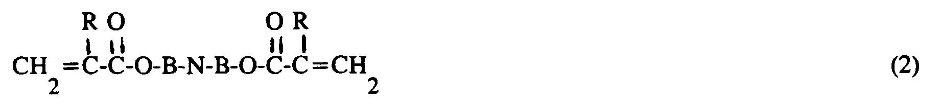
- the problem is solved in accordance with the invention by means of a method of manufacturing a laminated optical component having locally different properties, in which a substrate is provided with a coating having at least one patternwise defined section of a polymerized liquid crystalline monomer, whereby a uniform layer of the monomer is applied to the substrate, the monomer is oriented by an external force and the layer is irradiated in accordance with a pattern, so that the orientation of the liquid crystalline monomer is fixed as a consequence of polymerisation, after which the external force is changed and the layer is irradiated again, such that parts which were not irradiated in the first step are polymerised, thereby fixing the different orientation of the liquid crystalline monomer being present in latter parts, which monomer corresponds to the formula wherein
- N nematic or smectic groups
- substituents (Q) of the nematic/smectic group (N) are: cyano group, halogen atom, hydrogen atom, alkyl group having 1-8 carbon atoms, alkoxy group having 1-8 carbon atoms, nitro group, ammino group or an alkyl-substituted amino group in which the alkyl group comprises 1-4 carbon atoms.
- Suitable monomers are, in particular, liquid-crystalline diacrylates which are represented by the formula wherein R, B and N have the above-stated meaning.
- Suitable initiators are aromatic carbonyl compounds or a ketal such as benzil dimethyl ketal (Irgacure T.M.).
- each molecule comprises a nematic/smectic group N (formula 1). Due to the mobility and the presence of the group N a very rapid, substantially instantaneous orientation of the molecules can be attained by using an external force.
- the external force is a field of force such as an electric or magnetic field, the field direction of which can be readily adjusted, so that any desired orientation of the liquid-crystalline monomer compound can be obtained. It is alternatively possible to rub the substrate surface beforehand in one direction, such that the molecules of the liquid-crystalline monomer compound are subsequently oriented in the direction of rubbing. The orientation is fixed by polymerization of the liquid-crystalline monomer compound.
- the polymerization is carried out by exposure to light, in particular UV light.
- the monomer composition to be polymerized contains a photoinitiator which decomposes into radicals as a consequence of exposure, which radicals initiate the polymerization of the monomers.
- the photoinitiator is used in a quantity of from 1-5% by weight.
- suitable initiators can be represented by the following formulae:
- the oriented compound of formula 1 can be polymerized in a very short time, for example in a period of from a few seconds to maximally a few minutes.
- the component manufactured in accordance with the invention has changed properties in the patternwise defined section where the oriented and polymerized compound of formula 1 is present.
- This change of the properties is primarily determined by the choice of the compound of formula 1 and by the adjusted orientation.
- changed properties are: changed electric properties such as a changed electric conductivity, changed mechanical properties such as a different coefficient of expansion or a difference in hardness and resistance to wear.
- changed optical properties such as a changed refractive index, reflection and transmission.
- the refractive index and the absorption may differ substantially for different directions of polarization of light. Due to this, laminated optical components such as optical filters, in particular polarization filters, polarization beam splitters, optical gratings, waveguides, optical recording elements and integrated optical systems can be obtained by means of the method in accordance with the invention.
- liquid-crystalline diacrylate which corresponds to the above-stated formula 2 is used in the method in accordance with the invention.
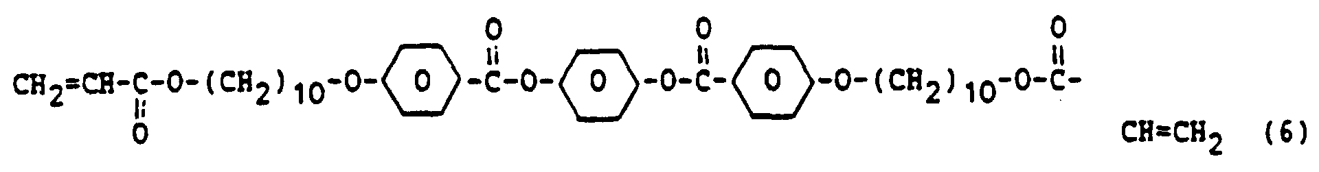
- Examples of effective liquid-crystalline diacrylates are represented in the above-stated formulae 3-6.
- diacrylates methacrylates
- a cross-linked structure is formed. This means that the orientation of the polymer molecules is preserved even at higher temperatures. Relaxation does not occur.
- a polymer layer constituting a mechanically very hard coating is obtained, for example, by imposing a direction of orientation of the monomer, and hence of the polymer, which extends parallel to the surface of the substrate.
- the external force used for orienting may be an external field of force. It is alternatively possible to rub the substrate surface beforehand in one direction.
- the pattern of the liquid-crystalline polymer is obtained by irradiating the monomer in accordance with a pattern.
- a uniform layer of the liquid-crystalline monomer is provided on the substrate, the liquid-crystalline monomer is oriented by an external force and the layer is irradiated in accordance with a pattern, the orientation of the liquid-crystalline compound being fixed as a consequence of polymerization.
- integrated optical systems such as an integrated waveguide colour filter can be manufactured readily.
- a uniform layer of the liquid-crystalline monomer is provided on the substrate, the liquid-crystalline monomer is oriented by an external field of force, the layer is irradiated in accordance with a pattern, so that the orientation of the liquid-crystalline monomer is fixed as a consequence of polymerization, subsequently the direction of the field of force is changed and the layer is irradiated again, such that the parts which were not irradiated in the first irradiation step are polymerized, the different orientation of the liquid-crystalline monomer present in these parts being fixed.
- two mutually different orientations are imposed on the polymer layer provided on the substrate.
- the above-said second irradiation step can also be carried out in accordance with a pattern and the direction of the field of force can be changed again after which a third irradiation step is carried out, so that a third orientation is obtained.
- this process can be repeated at will, so that in the end the substrate is provided with a polymer layer having many areas of mutually different orientations of the polymer molecules. This means that in numerous places of the substrate surface the properties can be imposed at will.
- the direction of the field of force is changed such that it is oppositely directed relative to the initial direction.
- the method in accordance with the invention is carried out such that after patterned irradiation, in which operation the oriented, liquid-crystalline monomer is polymerized, the temperature of the layer is increased so that the liquid-crystalline monomer in the unexposed portions of the layer is converted into the isotropic phase, and the layer is irradiated, so that the isotropic phase is fixed due to polymerization of the liquid-crystalline monomer.
- the invention further relates to a laminated component obtained by means of the method described above.
- the component in accordance with the invention comprises a substrate and a coating provided thereon, which coating comprises at least one patternwise defined section of an oriented and radiation-polymerized liquid-crystalline monomer which corresponds to the above-stated formula 1.
- the coating comprises a dichroic dye.
- This component can suitably be used as an optical filter and, in particular, as a polarization filter.
- Suitable dichroic dyes are represented by the formulae wherein R represents an aklyl group.
- the section which is defined in accordance with a pattern is an information bit which can be read optically.
- the laminated component is an optical recording element in which, in the presence of an electric or magnetic field, information can be recorded by means of modulated laser light and read by means of low-energy continuous laser light.
- the layer of the liquid-crystalline monomer of formula 1 is oriented by the electric or magnetic field. In the areas irradiated by modulated laser light, said areas having diametral dimensions of, for example, 1-3 micron, polymerization takes place so that the orientation is fixed. These areas (bits) can be read by means of low-energy laser light on the basis of, for example, reflection differences with the surroundings.
- a layer 2 of a mixture of liquid-crystalline monomer compounds is provided on a glass or polymethyl methacrylate substrate which is indicated by reference numeral 1.
- the mixture comprises 20% by weight of a compound of formula 3, 79% by weight of a compound of formula 4, and 1% by weight of benzil dimethyl ketal (initiator, Irgacure T.M).
- the layer thickness amounts to 10 ⁇ m.
- the surface of substrate 1 is rubbed in the direction indicated by an arrow 3.
- the Y-shaped portion 5 forms a light conductor, a light beam 8 incident on surface 7 remaining within the Y-shape and being divided into two sub-beams 10, 11 at the bifurcation 9 of the Y-shape.
- a coating having a low refractive index may be applied to the Y-splitter obtained, or the layer 2 of liquid-crystalline compounds may be provided between two glass plates or synthetic resin plates.
- the molecules of the liquid-crystalline monomer compound are oriented in a direction parallel to the magnetic field direction under the influence of a magnetic field of 10 k.Gauss having a field direction which is indicated by the arrow 14.
- the dichroic dye molecules are oriented correspondingly.
- the molecules extend perpendicularly to the surface of the Si substrate 12.
- An area 15 of layer 13 is subsequently exposed to UV light of 360 nm for a few minutes while the temperature and the magnetic field are preserved.
- the power of the low-pressure mercury vapour lamp used for this purpose is 5 mW/cm 2 . Due to exposure the oriented monomer molecules in the area 15 of layer 13 are polymerized so that the orientation is fixed.
- the direction of the magnetic field is changed such that the field direction, indicated by arrow 16, is parallel to the surface of layer 13. Consequently, the orientation of the molecules of the liquid-crystalline monomer compound outside the area 15 changes such that the molecules are oriented parallel to the surface of layer 13, in the direction indicated by arrow 17.
- This direction of orientation corresponds to the direction of the magnetic field applied.
- the areas 18 and 19 of layer 13 which are situated on either side of the area 15 are exposed to UV light in the same manner as area 15. Due to exposure, the molecules of the monomer compound present in the areas 18 and 19 are polymerized. In this process, the direction of orientation is fixed.
- the unexposed portion of layer 13 is removed by means of immersion in tetrahydrofuran.
- a layer 20 of polymethyl methacrylate is provided instead.
- This layer is provided by means of a spin-coating operation in which a 20% solution of polymethyl methacrylate in ethyl acetate is used.
- the refractive index of the oriented areas 15, 18 and 19 is 1.68 in a direction parallel to the direction of orientation, and 1.53 in the direction perpendicular to the direction of orientation.
- the refractive index of the area 20 is 1.49. This means that the areas 15, 18 and 19 together form a waveguide.
- Light which is incident via surface 21 is conducted through layer 13 of the element via the areas 18, 15, 19.
- the vertical polarization component of the incident light is absorbed by the oriented dye molecules.
- Horizontally polarized light is transmitted and leaves the element at the surface 22 of area 19, which is located opposite surface 21.
- reference numeral 23 denotes a substrate of glass which is provided with a layer 24 of a liquid-crystalline mixture comprising 98.5% by weight of a monomer compound, represented by formula 5, and 1.5% by weight of the initiator represented by formula 7.
- the layer thickness amounts to 100 ⁇ m.
- layer 24 is oriented in the direction indicated by the arrow 25 in the same manner as described with respect to the preceding Figures. The said orientation is carried out at a temperature exceeding the transition temperature from the crystalline to the nematic phase, at 140° C. Layer 24 is exposed to UV light according to a pattern so that polymerization of the monomer molecules in the exposed area 26 takes place. In this process, the direction of orientation of these molecules is fixed.
- the temperature of layer 24 is reduced from 140° C to 100° C. Due to this, the degree of orientation and the double refraction are increased. As a consequence hereof, the component of the refractive index which extends perpendicularly to the molecular axis decreases. The entire surface of layer 24 is then exposed to UV light. As a consequence hereof, the higher degree of orientation in the areas 33 and 34 is fixed. These areas have a refractive index of 1.53.
- the anisotropic area 26 has a refractive index of 1.54.
- the anisotropic areas 29 and 31 have two refractive indices (n o and n e ) of 1.53 and 1.69, respectively, for the direction of propagation of light.
- reference numeral 40 denotes a substrate plate of polycarbonate which is provided on one side with a spiral-shaped groove 41 which forms a follower track for optically scanning the plate.
- a reflection layer of Al is provided on the surface in which a follower track is formed.
- On top of this reflection layer there is a thin layer 42 of a liquid-crystalline monomer compound, as represented by formula 3.
- the layer 42 also contains 1.5% by weight of a benzil dimethyl ketal as an initiator.
- the layer 42 of the monomer compound is oriented in a magnetic field, the field direction of which is indicated by arrow 43.
- the monomer molecules are oriented in a direction perpendicular to the surface of the plate.
- This orientation takes place at a temperature which is higher than the transition temperature crystalline-nematic.
- a suitable temperature is 110° C.
- the monomer layer is scanned with a low-energy laser light beam indicated by reference numeral 44. This beam does not bring about changes in the monomer layer 42 because no absorption of light takes place.
- the laser light is used only to follow the follower track on the basis of phase differences in the reflected light emanating from the track and from the environment of the track.
- a second laser light beam 45 is coupled, via for example a common housing 46, to the first laser light beam, the light spot emanating from the second beam being moved relative to that of the first beam in a radial direction relative to the plate, for example over a distance equal to half the combined width of the groove 41 and the land part 47 situated between the groove turns.
- the second laser light beam is pulsated in conformity with the information to be recorded. Polymerization of the monomer compound takes place in the irradiated areas of layer 42. In this process, the direction of orientation of the compound is fixed. Consequently, information bits of oriented and polymerized material are formed. After recording the information the magnetic field is switched off.
- unoriented domains of the liquid-crystalline compound will be formed in the portion of layer 42 located outside the information bits. This area will exhibit dynamic scattering.
- the information bits can be read optically on the basis of reflection differences with the surrounding area of LC domains exhibiting dynamic scattering.
- the temperature of the entire layer 42 can be raised to, for example, 160°C after information has been recorded, such that the area outside the information bits exhibits an isotropic phase. By irradiating the entire surface of layer 42, the isotropic phase can be fixed due to polymerization of the isotropic monomer compound.
- the oriented information bits can be read optically on the basis of reflection differences with the isotropic environment.
- reference numeral 50 denotes an aluminium matrix having a rectangular cross-section of 80 x 60 mm and a height of 10 mm.
- Two parallel grooves 51 and 52 having a depth of 1 mm are provided in the upper surface of matrix 50.
- the upper surface of the matrix 50 is covered with a very thin polyimide layer 53.
- the matrix is heated in a vacuum to a temperature of 350° C for 1 hour. Subsequently, the polyimide layer is rubbed in a direction parallel to the grooves by means of a nylon brush.
- the matrix is heated to a temperature of 130° C.
- a thin layer which is not shown, of a liquid-crystalline monomer A, corresponding to the above-stated formula 6, and comprising 1% by weight of a photoinitiator in accordance with formula 8, is applied to the heated matrix.
- a glass plate 54 having a thickness of 12 mm is provided on the monomer layer A.
- the glass plate is provided with a UV-light cured layer, which is not shown, of a liquid-crystalline monomer.
- a glass plate which is provided with such a layer is obtained by providing the surface with a 2% solution in tetrahydrofuran of a UV-light curable composition I comprising 60 parts by weight of a liquid-crystalline monomer compound of formula 11, 36 parts by weight of a monomer in accordance with formula 12, and 4 parts by weight of a photo-initiator in accordance with formula 8. 1.58.
- the incident unpolarized light beam 59 passes through the isotropic polymer layer 58 until it reaches the rod 55 of oriented polymer. At this location a bifurcation of the light beam 59 takes place, the direction depending on the two directions of polarization of light beam 59.
- the light having a direction of polarization 62 which is perpendicular to the orientation of rod 55 is reflected according to Fresnel's law, the polarized light beam 63 being formed. At this stage, the essential function of a polarization beam splitter is attained. However, for many applications it is desirable that both polarized light beams 61 and 63 are parallel. To realize this a second rod 56 of oriented polymer is provided such that beam 64 extends parallel to beam 61.
- the glass plate which has been provided with an oriented polymer layer B in the above-described manner, is provided on the layer of monomer A
- this monomer is exposed to UV light via the glass plate at a temperature of 130° C.
- the monomer A is oriented by contacting the oriented polyimide layer 53. This degree of orientation of the molecules of monomer A is increased due to the contact with the oriented polymer layer B of the glass plate. As a consequence of exposure to UV light the monomer A polymerizes into an oriented polymer. After the matrix is removed a product in accordance with Fig. 6 is obtained.
- reference numeral 54 denotes the glass plate which is provided with lands 55 and 56 of oriented polymer on one side.
- a second glass plate 57 is provided on the lands and the space between the glass plates is filled with the above-described curable, isotropic, composition I, by capillary suction.
- the polarization beam splitter obtained is shown in Fig. 7.
- the rods 55, 56 are manufactured from an oriented liquid-crystalline polymer having an anisotropic refractive index which can be split up into two components, namely the refractive index n e for the plane parallel with the direction of orientation of the rods, and n o for the plane perpendicular to the direction of orientation.
- the refractive index n o has a value of 1.49 and n e has a value of
Landscapes
- Physics & Mathematics (AREA)
- Chemical & Material Sciences (AREA)
- General Physics & Mathematics (AREA)
- Engineering & Computer Science (AREA)
- Crystallography & Structural Chemistry (AREA)
- Nonlinear Science (AREA)
- Optics & Photonics (AREA)
- Spectroscopy & Molecular Physics (AREA)
- Organic Chemistry (AREA)
- Microelectronics & Electronic Packaging (AREA)
- Materials Engineering (AREA)
- Manufacturing & Machinery (AREA)
- Mathematical Physics (AREA)
- Addition Polymer Or Copolymer, Post-Treatments, Or Chemical Modifications (AREA)
- Liquid Crystal (AREA)
- Compositions Of Macromolecular Compounds (AREA)
- Polarising Elements (AREA)
- Laminated Bodies (AREA)
Claims (9)
- Verfahren zum herstellen eines optischen verbundelementes mit örtlich verschiedenen Eigenschaften, wobei ein Träger vorgesehen ist mit einer Deckschicht mit wenigstens einem mustermäßig definierten Gebietsteil aus einem polymerisierten flüssigkristallinen Monomer, wobei eine einheitliche Schicht des Monomers auf dem Träger angebracht wird, das Monomer durch eine äußere Kraft mustermäßig bestrahlt wird, so daß die Orientierung des flüssigkristallinen Monomers infolge der Polymerisierung festgelegt wird, wonach die äußere Kraft geändert und die Schicht wieder bestrahlt wird, so daß Teile, die in dem ersten Schritt nicht bestrahlt wurden, polymerisiert werden, wodurch die andere Orientierung des flüssigkristallinen Monomers in diesen letzten Teilen fixiert wird, wobei dieses Monomer der nachstehenden Formel entspricht
 P eine polymerisierbare Gruppe ist,B eine Verbindungsgruppe istN eine nematische oder smektische flüssigkristalline Gruppe ist, die mindestens eine p-Phenylen- und/oder Zyklohexylgruppe aufweist,Q ein Substituent der Gruppe BN ist, wobei N und B die obengenannte Bedeutung haben, wobei das genannte Monomer zusammen mit einem Initiator verwendet wird.
 - Verfahren nach Anspruch 1, dadurch gekennzeichnet, daß das Monomer der nachstehenden Formel entspricht:
- Verfahren nach Anspruch 2, dadurch gekennzeichnet, daß ein Monomer verwendet wird, das aus einer oder mehreren Verbindungen der nachfolgenden Formeln verwendet wird, das aus einer oder mehreren Verbindungen der nachfolgenden Formeln selektiert worden ist:


- Verfahren nach Anspruch 1, 2 oder 3, dadurch gekennzeichnet, daß die Richtung des Kraftfeldes derart geändert wird, daß diese der ursprünglichen Richtung entgegengesetzt ist.
- Verfahren nach Anspruch 1, 2, 3 oder 4, dadurch gekennzeichnet, daß nach Bestrahlung die Temperatur der Schicht aus dem flüssigkristallinen Monomer gesteigert wird, wobei das flüssigkristalline Monomer in den nicht-bestrahlten Teilen der Schicht in die isotrope Phase gebracht und die Schicht bestrahlt wird, wobei durch die Polymerisierung des flüssigkristallinen Monomers die isotrope Phase festgelegt wird.
- Verbundelement mit örtlich abweichenden Eigenschaften, das nach dem Verfahren nach einem der vorhergehenden Ansprüche 1 bis 5 hergestellt ist, dadurch gekennzeichnet, daß das Elenment einen Träger und eine Deckschicht aufweist mit wenigstens einem mustermäßig definierten Teil, der aus einem orientierten und strahlungspolymerisierten flüssigkristallinen Monomer besteht, das der Formel 1 entspricht.
- Verbundelement nach Anspruch 6, dadurch gekennzeichnet, daß die Deckschicht den (die) mustermäßig definierten Teil(e) aufweist, in denen das flüssigkristalline Polymer in der orientierten Konfiguration vorhanden ist und ein restlicher Gebietsteil, in dem sich das Polymer befindet, in einer isotropen Konfiguration vorhanden ist.
- Verbundelement nach Anspruch 6 oder 7, dadurch gekennzeichnet, daß die deckschicht einen zweifarbigen Farbstoff aufweist.
- Verbundelement nach Anspruch 6 oder 7, dadurch gekennzeichnet, daß der mustermäßig definierte Teil ein Informationsbit bildet, das optisch ausgelesen werden kann.
Applications Claiming Priority (4)
| Application Number | Priority Date | Filing Date | Title |
|---|---|---|---|
| NL8800512 | 1988-02-29 | ||
| NL8800512 | 1988-02-29 | ||
| NL8802832 | 1988-11-17 | ||
| NL8802832A NL8802832A (nl) | 1988-02-29 | 1988-11-17 | Methode voor het vervaardigen van een gelaagd element en het aldus verkregen element. |
Publications (3)
| Publication Number | Publication Date |
|---|---|
| EP0331233A2 EP0331233A2 (de) | 1989-09-06 |
| EP0331233A3 EP0331233A3 (de) | 1991-10-30 |
| EP0331233B1 true EP0331233B1 (de) | 1997-04-23 |
Family
ID=26646356
Family Applications (1)
| Application Number | Title | Priority Date | Filing Date |
|---|---|---|---|
| EP89200427A Expired - Lifetime EP0331233B1 (de) | 1988-02-29 | 1989-02-22 | Verfahren zum Herstellen eines optischen Verbundelements und das auf diese Weise erhaltene Element |
Country Status (6)
| Country | Link |
|---|---|
| US (1) | US4983479A (de) |
| EP (1) | EP0331233B1 (de) |
| JP (1) | JP2849672B2 (de) |
| KR (1) | KR0147367B1 (de) |
| DE (1) | DE68927986T2 (de) |
| NL (1) | NL8802832A (de) |
Cited By (11)
| Publication number | Priority date | Publication date | Assignee | Title |
|---|---|---|---|---|
| US7044600B2 (en) | 2004-01-14 | 2006-05-16 | Ppg Industries Ohio, Inc. | Polarizing devices and methods of making the same |
| US7256921B2 (en) | 2003-07-01 | 2007-08-14 | Transitions Optical, Inc. | Polarizing, photochromic devices and methods of making the same |
| US7342112B2 (en) | 2003-07-01 | 2008-03-11 | Ppg Industries Ohio, Inc. | Photochromic compounds |
| US7632540B2 (en) | 2003-07-01 | 2009-12-15 | Transitions Optical, Inc. | Alignment facilities for optical dyes |
| US7879256B2 (en) | 2006-03-31 | 2011-02-01 | E. I. Du Pont De Nemours And Company | Liquid crystal compositions, polymer networks derived therefrom and process for making the same |
| US7914700B2 (en) | 2006-03-31 | 2011-03-29 | E. I. Du Pont De Nemours And Company | Liquid crystal compositions and polymer networks derived therefrom |
| US7978391B2 (en) | 2004-05-17 | 2011-07-12 | Transitions Optical, Inc. | Polarizing, photochromic devices and methods of making the same |
| US8077373B2 (en) | 2003-07-01 | 2011-12-13 | Transitions Optical, Inc. | Clear to circular polarizing photochromic devices |
| CN102884158A (zh) * | 2010-04-27 | 2013-01-16 | 住友化学株式会社 | 组合物 |
| US9096014B2 (en) | 2003-07-01 | 2015-08-04 | Transitions Optical, Inc. | Oriented polymeric sheets exhibiting dichroism and articles containing the same |
| US10866455B2 (en) | 2017-10-19 | 2020-12-15 | Ppg Industries Ohio, Inc. | Display devices including photochromic-dichroic compounds and dichroic compounds |
Families Citing this family (65)
| Publication number | Priority date | Publication date | Assignee | Title |
|---|---|---|---|---|
| EP0423880B1 (de) * | 1989-10-18 | 1995-03-01 | Koninklijke Philips Electronics N.V. | Molekular orientierte Kunststoffzusammensetzung |
| JPH05502950A (ja) * | 1989-12-26 | 1993-05-20 | アライド―シグナル・インコーポレーテッド | 光学活性導波路の製造法 |
| US5073294A (en) * | 1990-03-07 | 1991-12-17 | Hercules Incorporated | Process of preparing compositions having multiple oriented mesogens |
| DE69215565T2 (de) * | 1991-03-26 | 1997-05-28 | Philips Electronics Nv | Flüssigkristallbildwiedergabeanordnung mit Orientierungsschicht |
| DE59209315D1 (de) * | 1991-07-26 | 1998-06-10 | Rolic Ag | Flüssigkristall-Zelle |
| US6160597A (en) * | 1993-02-17 | 2000-12-12 | Rolic Ag | Optical component and method of manufacture |
| DE59408097D1 (de) * | 1993-02-17 | 1999-05-20 | Rolic Ag | Orientierungsschicht für Flüssigkristalle |
| SG50569A1 (en) * | 1993-02-17 | 2001-02-20 | Rolic Ag | Optical component |
| US6258974B1 (en) * | 1993-04-13 | 2001-07-10 | Southwest Research Institute | Metal oxide compositions composites thereof and method |
| KR100331127B1 (ko) * | 1994-02-15 | 2002-10-18 | 내셔널 세미콘덕터 코포레이션 | 표준cmos공정용고전압cmos트랜지스터 |
| DE4408171A1 (de) * | 1994-03-11 | 1995-09-14 | Basf Ag | Neue polymerisierbare flüssigkristalline Verbindungen |
| DE4408170A1 (de) * | 1994-03-11 | 1995-09-14 | Basf Ag | Neue polymerisierbare flüssigkristalline Verbindungen |
| DE59509361D1 (de) | 1994-06-24 | 2001-08-02 | Rolic Ag Zug | Optisches Bauelement |
| DE59510708D1 (de) | 1994-06-24 | 2003-07-10 | Rolic Ag Zug | Optisches Bauelement aus Schichten vernetzter flüssigkristalliner Monomere und Verfahren zu seiner Herstellung |
| GB2293249A (en) | 1994-09-09 | 1996-03-20 | Sharp Kk | Polarisation sensitive device and a method of manufacture thereof |
| US5593617A (en) * | 1994-09-12 | 1997-01-14 | Hoffmann-Laroche Inc. | Photochemically polymerizable liquid crystals |
| EP0794991B1 (de) * | 1994-12-03 | 2000-11-08 | MERCK PATENT GmbH | Cholesterisches polymernetzwerk |
| JP2820051B2 (ja) * | 1995-01-30 | 1998-11-05 | 日本電気株式会社 | レジスト材料 |
| AU4620396A (en) * | 1995-02-06 | 1996-08-27 | Merck Patent Gmbh | Direactive mesogenic compounds and intermediates |
| EP0731084B1 (de) * | 1995-03-03 | 2002-09-25 | Rolic AG | Photovernetzbare Naphthylderivate |
| EP0729952A1 (de) * | 1995-03-03 | 1996-09-04 | F. Hoffmann-La Roche Ag | 1-Fluorcyclohexen-Dioxan Derivate |
| DE59605843D1 (de) * | 1995-07-28 | 2000-10-12 | Rolic Ag Zug | Photovernetzbare flüssigkristalline 1,2-Phenylen-Derivate |
| DE59608943D1 (de) * | 1995-07-28 | 2002-05-02 | Rolic Ag Zug | Photovernetzbare flüssigkristalline 1,4-Dioxan-2,3-diyl-Derivate |
| GB2305925B (en) * | 1995-10-06 | 1999-10-13 | Merck Patent Gmbh | Anistropic polymer |
| US5903330A (en) * | 1995-10-31 | 1999-05-11 | Rolic Ag | Optical component with plural orientation layers on the same substrate wherein the surfaces of the orientation layers have different patterns and direction |
| GB2315073B (en) * | 1996-07-04 | 2000-04-19 | Patent Gmbh Merck | Linear UV polariser |
| US5773178A (en) * | 1996-09-13 | 1998-06-30 | Japan Synthetic Rubber Co, Ltd. | Process for producing a patterned anisotropic polymeric film |
| US5928819A (en) * | 1996-12-19 | 1999-07-27 | Xerox Corporation | Methods to fabricate optical equivalents of fiber optic face plates using reactive liquid crystals and polymers |
| GB2321717A (en) | 1997-01-31 | 1998-08-05 | Sharp Kk | Cholesteric optical filters |
| US6124970A (en) * | 1997-10-20 | 2000-09-26 | Latents Image Technology Ltd. | Polymer materials with latent images visible in polarized light and methods for their production |
| JP2002521354A (ja) * | 1998-07-24 | 2002-07-16 | ロリク アーゲー | 架橋性液晶化合物 |
| JP2001133630A (ja) | 1999-11-04 | 2001-05-18 | Fuji Photo Film Co Ltd | 異方性膜及び液晶表示素子 |
| US6546163B2 (en) * | 2000-10-09 | 2003-04-08 | John I. Thackara | Planar waveguide switch and optical cross-connect |
| EP1281728A1 (de) * | 2001-07-16 | 2003-02-05 | Dsm N.V. | Flexible Folie mit Sperreigenschaften |
| US6778753B2 (en) * | 2001-07-25 | 2004-08-17 | E. I. Du Pont De Nemours And Company | Halogenated optical polymer composition |
| US6919946B2 (en) | 2002-04-16 | 2005-07-19 | 3M Innovative Properties Company | Compensators for liquid crystal displays and the use and manufacture of the compensators |
| JP2005530300A (ja) * | 2002-06-19 | 2005-10-06 | コーニンクレッカ フィリップス エレクトロニクス エヌ ヴィ | ガラス基質における予めの配向を利用した多層光記憶装置 |
| EP1400838A1 (de) * | 2002-09-19 | 2004-03-24 | Rolic AG | Dünnschichten mit geriffelter Oberflächentopologie und Herstellungsverfahren |
| US8698117B2 (en) | 2003-07-01 | 2014-04-15 | Transitions Optical, Inc. | Indeno-fused ring compounds |
| US8545984B2 (en) | 2003-07-01 | 2013-10-01 | Transitions Optical, Inc. | Photochromic compounds and compositions |
| US8211338B2 (en) | 2003-07-01 | 2012-07-03 | Transitions Optical, Inc | Photochromic compounds |
| US8582192B2 (en) | 2003-07-01 | 2013-11-12 | Transitions Optical, Inc. | Polarizing photochromic articles |
| US20110140056A1 (en) * | 2003-07-01 | 2011-06-16 | Transitions Optical, Inc. | Indeno-fused ring compounds |
| US8518546B2 (en) | 2003-07-01 | 2013-08-27 | Transitions Optical, Inc. | Photochromic compounds and compositions |
| US7390540B2 (en) | 2004-07-21 | 2008-06-24 | Hewlett-Packard Development Company, L.P. | Method for preparation of anisotropic materials |
| US7296389B2 (en) * | 2005-03-28 | 2007-11-20 | Hitachi Global Storage Technologies Netherlands Bv | System, method, and apparatus for removing covers from shipping containers |
| EP1904301A2 (de) * | 2005-05-26 | 2008-04-02 | E.I. Dupont De Nemours And Company | Verdrillte nematische flüssigkristalle enthaltende hochfeste mehrlagige laminate |
| JP2008542065A (ja) * | 2005-05-26 | 2008-11-27 | イー・アイ・デュポン・ドウ・ヌムール・アンド・カンパニー | ねじれネマチック液晶を含む多層ラミネート |
| DE102005063524B4 (de) * | 2005-07-08 | 2011-01-27 | Grau, Günter, Dr. | Vorrichtung zur Messung und Erzeugung der Polarisation von Licht |
| JP2009522399A (ja) | 2005-12-29 | 2009-06-11 | イー・アイ・デュポン・ドウ・ヌムール・アンド・カンパニー | 赤外線の透過を低減するための組成物 |
| JP5186116B2 (ja) * | 2006-06-12 | 2013-04-17 | 富士フイルム株式会社 | 化合物、それを含有する液晶組成物、異方性材料、偏光板保護フィルム、光学補償フィルムならびに液晶表示装置 |
| EP2094815B1 (de) | 2006-12-22 | 2012-06-27 | Rolic AG | Strukturierbares flüssigkristall polymer mit thioethereinheiten |
| JP5408841B2 (ja) * | 2006-12-29 | 2014-02-05 | 株式会社Adeka | 重合性化合物及び重合性組成物 |
| WO2009005330A2 (en) * | 2007-07-05 | 2009-01-08 | Lg Chem, Ltd. | Composition comprising curable dichroic dye for forming ptical component and an optical component prepared using the same |
| WO2009023762A1 (en) | 2007-08-15 | 2009-02-19 | E. I. Du Pont De Nemours And Company | Alkaloid monomers, liquid crystal compositions and polymer networks derived therefrom |
| JP2010536782A (ja) | 2007-08-15 | 2010-12-02 | イー・アイ・デュポン・ドウ・ヌムール・アンド・カンパニー | キラル化合物、液晶組成物およびそれらから誘導されるポリマー網状構造 |
| CN101903494B (zh) | 2007-12-21 | 2016-03-02 | 罗利克有限公司 | 光校准组合物 |
| EP2222740B1 (de) | 2007-12-21 | 2017-10-11 | Rolic AG | Funktionalisierte lichtreaktive verbindungen |
| US20090324799A1 (en) * | 2008-05-15 | 2009-12-31 | Robert Michael Hartman | Maximizing utilization of municipal sewage treatment effluents to produce a biofuel, fertilizer and/or animal feed for environmentally sustainable minded communities |
| US7988881B2 (en) | 2008-09-30 | 2011-08-02 | E. I. Du Pont De Nemours And Company | Multilayer laminates comprising chiral nematic liquid crystals |
| JP5691808B2 (ja) * | 2011-04-28 | 2015-04-01 | 住友大阪セメント株式会社 | 光導波路デバイス |
| GB201110948D0 (en) * | 2011-06-28 | 2011-08-10 | Univ Gent | Methods and systems for trimming photonic devices |
| JP2017518413A (ja) | 2014-05-21 | 2017-07-06 | ロリク アーゲーRolic Ag | 重合性二色性染料 |
| KR102326314B1 (ko) | 2015-02-06 | 2021-11-12 | 삼성전자주식회사 | 중합성 액정 화합물 및 이를 포함하는 보상필름, 반사 방지 필름과 표시장치 |
| JP6312894B1 (ja) | 2017-04-11 | 2018-04-18 | 株式会社フジクラ | バンドパスフィルタ |
Family Cites Families (14)
| Publication number | Priority date | Publication date | Assignee | Title |
|---|---|---|---|---|
| US3804618A (en) * | 1967-06-16 | 1974-04-16 | Xerox Corp | Liquid crystal imaging system |
| US3794491A (en) * | 1972-06-14 | 1974-02-26 | Eastman Kodak Co | Amplification of low-density polyyne images |
| US4439514A (en) * | 1979-06-25 | 1984-03-27 | University Patents, Inc. | Photoresistive compositions |
| US4615962A (en) * | 1979-06-25 | 1986-10-07 | University Patents, Inc. | Diacetylenes having liquid crystal phases |
| FR2568568A1 (fr) * | 1984-08-01 | 1986-02-07 | Corning Glass Works | Perfectionnement a la fabrication de verres stratifies transparents polarisants et verres ainsi obtenus |
| FR2572813A1 (fr) * | 1984-11-07 | 1986-05-09 | Armstrong World Ind Inc | Procede pour preparer des revetements liquides polymeres presentant des reponses optiques multiples et revetements ainsi obtenus |
| JPH0718995B2 (ja) * | 1985-02-19 | 1995-03-06 | キヤノン株式会社 | 液晶素子 |
| US4683327A (en) * | 1985-06-24 | 1987-07-28 | Celanese Corporation | Anisotropic heat-curable acrylic terminated monomers |
| US4618514A (en) * | 1985-12-20 | 1986-10-21 | Rca Corporation | Alignment layer for liquid crystal display |
| US4820026A (en) * | 1986-03-20 | 1989-04-11 | Canon Kabushiki Kaisha | Ferroelectric liquid crystal device with modified polyvinyl alcohol alignment film |
| EP0261712A1 (de) * | 1986-09-04 | 1988-03-30 | Koninklijke Philips Electronics N.V. | Bildanzeigezelle, Verfahren zur Herstellung einer orientierenden Schicht über ein Substrat dieser Bildanzeigezelle und Monomer-Verbindung für ihre Anwendung als orientierende Schicht |
| JPS63129323A (ja) * | 1986-11-20 | 1988-06-01 | Asahi Glass Co Ltd | 液晶表示素子 |
| US4818070A (en) * | 1987-01-22 | 1989-04-04 | Asahi Glass Company Ltd. | Liquid crystal optical device using U.V.-cured polymer dispersions and process for its production |
| US4938568A (en) * | 1988-01-05 | 1990-07-03 | Hughes Aircraft Company | Polymer dispersed liquid crystal film devices, and method of forming the same |
-
1988
- 1988-11-17 NL NL8802832A patent/NL8802832A/nl not_active Application Discontinuation
-
1989
- 1989-02-22 DE DE68927986T patent/DE68927986T2/de not_active Expired - Fee Related
- 1989-02-22 EP EP89200427A patent/EP0331233B1/de not_active Expired - Lifetime
- 1989-02-24 US US07/315,066 patent/US4983479A/en not_active Expired - Lifetime
- 1989-02-25 KR KR1019890002240A patent/KR0147367B1/ko not_active Expired - Fee Related
- 1989-02-28 JP JP1045526A patent/JP2849672B2/ja not_active Expired - Fee Related
Cited By (32)
| Publication number | Priority date | Publication date | Assignee | Title |
|---|---|---|---|---|
| US7847998B2 (en) | 2003-07-01 | 2010-12-07 | Transitions Optical, Inc. | Polarizing, photochromic devices and methods of making the same |
| US7457025B2 (en) | 2003-07-01 | 2008-11-25 | Transitions Optical, Inc. | Polarizing, photochromic devices and methods of making the same |
| US10619018B2 (en) | 2003-07-01 | 2020-04-14 | Transitions Optical, Inc. | Oriented polymeric sheets exhibiting dichroism and articles containing the same |
| US7256921B2 (en) | 2003-07-01 | 2007-08-14 | Transitions Optical, Inc. | Polarizing, photochromic devices and methods of making the same |
| US7286275B2 (en) | 2003-07-01 | 2007-10-23 | Transitions Optical, Inc. | Polarizing, photochromic devices and methods of making the same |
| US7342112B2 (en) | 2003-07-01 | 2008-03-11 | Ppg Industries Ohio, Inc. | Photochromic compounds |
| US7349137B2 (en) | 2003-07-01 | 2008-03-25 | Ppg Industries Ohio, Inc. | Polarizing, photochromic devices and methods of making the same |
| US7349138B2 (en) | 2003-07-01 | 2008-03-25 | Ppg Industries Ohio, Inc. | Polarizing, photochromic devices and methods of making the same |
| US7505189B2 (en) | 2003-07-01 | 2009-03-17 | Transitions Optical, Inc. | Polarizing, photochromic devices and methods of making the same |
| US7394585B2 (en) | 2003-07-01 | 2008-07-01 | Ppg Industries Ohio, Inc. | Polarizing, photochromic devices and methods of making the same |
| US7429105B2 (en) | 2003-07-01 | 2008-09-30 | Ppg Industries Ohio, Inc. | Polarizing, photochromic devices and methods of making the same |
| US8077373B2 (en) | 2003-07-01 | 2011-12-13 | Transitions Optical, Inc. | Clear to circular polarizing photochromic devices |
| US7466469B2 (en) | 2003-07-01 | 2008-12-16 | Ppg Industries Ohio, Inc. | Polarizing, photochromic devices and methods of making the same |
| US7471436B2 (en) | 2003-07-01 | 2008-12-30 | Transitions Optical, Inc. | Polarizing, photochromic devices and methods of making the same |
| US10007038B2 (en) | 2003-07-01 | 2018-06-26 | Transitions Optical, Inc. | Optical elements with alignment facilities for optical dyes |
| US9096014B2 (en) | 2003-07-01 | 2015-08-04 | Transitions Optical, Inc. | Oriented polymeric sheets exhibiting dichroism and articles containing the same |
| US7359104B2 (en) | 2003-07-01 | 2008-04-15 | Ppg Industries Ohio, Inc. | Polarizing, photochromic devices and methods of making the same |
| US7632540B2 (en) | 2003-07-01 | 2009-12-15 | Transitions Optical, Inc. | Alignment facilities for optical dyes |
| US8926091B2 (en) | 2003-07-01 | 2015-01-06 | Transitions Optical, Inc. | Optical elements with alignment facilities for optical dyes |
| US8089678B2 (en) | 2003-07-01 | 2012-01-03 | Transitions Optical, Inc | Clear to circular polarizing photochromic devices and methods of making the same |
| US8003005B2 (en) | 2003-07-01 | 2011-08-23 | Transitions Optical, Inc. | Alignment facilities for optical dyes |
| US7044600B2 (en) | 2004-01-14 | 2006-05-16 | Ppg Industries Ohio, Inc. | Polarizing devices and methods of making the same |
| US7097304B2 (en) | 2004-01-14 | 2006-08-29 | Transitions Optical Inc. | Polarizing devices and methods of making the same |
| US7097303B2 (en) | 2004-01-14 | 2006-08-29 | Ppg Industries Ohio, Inc. | Polarizing devices and methods of making the same |
| US7978391B2 (en) | 2004-05-17 | 2011-07-12 | Transitions Optical, Inc. | Polarizing, photochromic devices and methods of making the same |
| US8334393B2 (en) | 2006-03-31 | 2012-12-18 | E I Du Pont De Nemours And Company | Chiral compounds and liquid crystal compositions and polymer networks derived therefrom |
| US8344175B2 (en) | 2006-03-31 | 2013-01-01 | E I Du Pont De Nemours And Company | Liquid crystal compositions, polymer networks derived therefrom and process for making the same |
| US7914700B2 (en) | 2006-03-31 | 2011-03-29 | E. I. Du Pont De Nemours And Company | Liquid crystal compositions and polymer networks derived therefrom |
| US7879256B2 (en) | 2006-03-31 | 2011-02-01 | E. I. Du Pont De Nemours And Company | Liquid crystal compositions, polymer networks derived therefrom and process for making the same |
| CN102884158A (zh) * | 2010-04-27 | 2013-01-16 | 住友化学株式会社 | 组合物 |
| TWI494418B (zh) * | 2010-04-27 | 2015-08-01 | Sumitomo Chemical Co | 組成物 |
| US10866455B2 (en) | 2017-10-19 | 2020-12-15 | Ppg Industries Ohio, Inc. | Display devices including photochromic-dichroic compounds and dichroic compounds |
Also Published As
| Publication number | Publication date |
|---|---|
| DE68927986T2 (de) | 1997-11-06 |
| KR0147367B1 (ko) | 1998-09-15 |
| US4983479A (en) | 1991-01-08 |
| KR890013506A (ko) | 1989-09-23 |
| JPH026927A (ja) | 1990-01-11 |
| JP2849672B2 (ja) | 1999-01-20 |
| EP0331233A3 (de) | 1991-10-30 |
| DE68927986D1 (de) | 1997-05-28 |
| NL8802832A (nl) | 1989-09-18 |
| EP0331233A2 (de) | 1989-09-06 |
Similar Documents
| Publication | Publication Date | Title |
|---|---|---|
| EP0331233B1 (de) | Verfahren zum Herstellen eines optischen Verbundelements und das auf diese Weise erhaltene Element | |
| Shishido et al. | Rapid optical switching by means of photoinduced change in refractive index of azobenzene liquid crystals detected by reflection-mode analysis | |
| US4938568A (en) | Polymer dispersed liquid crystal film devices, and method of forming the same | |
| JP3945790B2 (ja) | 複屈折フィルムとその製造方法 | |
| EP0507880B1 (de) | Verfahren zur herstellung von optisch aktiven wellenleitern | |
| US5096282A (en) | Polymer dispersed liquid crystal film devices | |
| US20080089073A1 (en) | Dynamic Liquid Crystal Gel Holograms | |
| JP3626224B2 (ja) | 側鎖基重合体から製造した平板材料 | |
| JPH02210345A (ja) | 可逆的な光学的情報記憶方法および装置 | |
| DE3623395A1 (de) | Vorrichtung zur reversiblen, optischen datenspeicherung unter verwendung von polymeren fluessigkristallen | |
| US20060083866A1 (en) | Liquid crystalline film with broadened reflection bandwidth and process for preparation thereof | |
| JPH1048605A (ja) | 調光素子およびその製造方法 | |
| JP4048674B2 (ja) | 高分子膜に光学異方性を付与する方法、そのための装置および光学異方性媒体 | |
| US20060147810A1 (en) | Holographic optical elements, devices and methods | |
| KR100381565B1 (ko) | 액정조성물 및 이것을 중합시켜 수득된 고분자액정 | |
| JP2000515201A (ja) | 巨視的に配向した架橋ポリマーの製造方法 | |
| US6939587B1 (en) | Fabrication of aligned crystal cell/film by simultaneous alignment and phase separation | |
| JPS63216791A (ja) | レーザー光学的書き込み及び読み出し法、その装置及び多層レーザ光学的データディスク | |
| US20030096065A1 (en) | Efficient nonlinear optical polymers having high poling stability | |
| Uemura et al. | Birefringence and orientation direction control of photoalignable liquid crystalline copolymer films based on in situ modification of mesogenic groups | |
| Nevskaya et al. | Liquid-crystal-based microlasers | |
| KR100582990B1 (ko) | 액정을 이용한 편광 회절 소자 및 그 제조 방법 | |
| Ikeda et al. | Refractive-index modulation by means of photosensitive liquid crystals | |
| JP2007086673A (ja) | 光学素子 | |
| RU2242782C2 (ru) | Фоторефрактивный полимерный материал |
Legal Events
| Date | Code | Title | Description |
|---|---|---|---|
| PUAI | Public reference made under article 153(3) epc to a published international application that has entered the european phase |
Free format text: ORIGINAL CODE: 0009012 |
|
| AK | Designated contracting states |
Kind code of ref document: A2 Designated state(s): CH DE FR GB LI NL SE |
|
| PUAL | Search report despatched |
Free format text: ORIGINAL CODE: 0009013 |
|
| AK | Designated contracting states |
Kind code of ref document: A3 Designated state(s): CH DE FR GB LI NL SE |
|
| 17P | Request for examination filed |
Effective date: 19920429 |
|
| 17Q | First examination report despatched |
Effective date: 19950112 |
|
| GRAG | Despatch of communication of intention to grant |
Free format text: ORIGINAL CODE: EPIDOS AGRA |
|
| GRAH | Despatch of communication of intention to grant a patent |
Free format text: ORIGINAL CODE: EPIDOS IGRA |
|
| GRAH | Despatch of communication of intention to grant a patent |
Free format text: ORIGINAL CODE: EPIDOS IGRA |
|
| GRAA | (expected) grant |
Free format text: ORIGINAL CODE: 0009210 |
|
| AK | Designated contracting states |
Kind code of ref document: B1 Designated state(s): CH DE FR GB LI NL SE |
|
| REG | Reference to a national code |
Ref country code: CH Ref legal event code: EP |
|
| REF | Corresponds to: |
Ref document number: 68927986 Country of ref document: DE Date of ref document: 19970528 |
|
| ET | Fr: translation filed | ||
| PLBE | No opposition filed within time limit |
Free format text: ORIGINAL CODE: 0009261 |
|
| STAA | Information on the status of an ep patent application or granted ep patent |
Free format text: STATUS: NO OPPOSITION FILED WITHIN TIME LIMIT |
|
| 26N | No opposition filed | ||
| REG | Reference to a national code |
Ref country code: CH Ref legal event code: PFA Free format text: PHILIPS ELECTRONICS N.V. TRANSFER- KONINKLIJKE PHILIPS ELECTRONICS N.V. |
|
| NLT1 | Nl: modifications of names registered in virtue of documents presented to the patent office pursuant to art. 16 a, paragraph 1 |
Owner name: KONINKLIJKE PHILIPS ELECTRONICS N.V. |
|
| REG | Reference to a national code |
Ref country code: FR Ref legal event code: CD |
|
| REG | Reference to a national code |
Ref country code: GB Ref legal event code: IF02 |
|
| PGFP | Annual fee paid to national office [announced via postgrant information from national office to epo] |
Ref country code: FR Payment date: 20060224 Year of fee payment: 18 Ref country code: SE Payment date: 20060224 Year of fee payment: 18 |
|
| PGFP | Annual fee paid to national office [announced via postgrant information from national office to epo] |
Ref country code: GB Payment date: 20060227 Year of fee payment: 18 |
|
| PGFP | Annual fee paid to national office [announced via postgrant information from national office to epo] |
Ref country code: NL Payment date: 20060228 Year of fee payment: 18 |
|
| PGFP | Annual fee paid to national office [announced via postgrant information from national office to epo] |
Ref country code: DE Payment date: 20060418 Year of fee payment: 18 |
|
| PGFP | Annual fee paid to national office [announced via postgrant information from national office to epo] |
Ref country code: CH Payment date: 20060518 Year of fee payment: 18 |
|
| PG25 | Lapsed in a contracting state [announced via postgrant information from national office to epo] |
Ref country code: SE Free format text: LAPSE BECAUSE OF NON-PAYMENT OF DUE FEES Effective date: 20070223 |
|
| PG25 | Lapsed in a contracting state [announced via postgrant information from national office to epo] |
Ref country code: LI Free format text: LAPSE BECAUSE OF NON-PAYMENT OF DUE FEES Effective date: 20070228 Ref country code: CH Free format text: LAPSE BECAUSE OF NON-PAYMENT OF DUE FEES Effective date: 20070228 |
|
| REG | Reference to a national code |
Ref country code: CH Ref legal event code: PL |
|
| EUG | Se: european patent has lapsed | ||
| GBPC | Gb: european patent ceased through non-payment of renewal fee |
Effective date: 20070222 |
|
| NLV4 | Nl: lapsed or anulled due to non-payment of the annual fee |
Effective date: 20070901 |
|
| REG | Reference to a national code |
Ref country code: FR Ref legal event code: ST Effective date: 20071030 |
|
| PG25 | Lapsed in a contracting state [announced via postgrant information from national office to epo] |
Ref country code: DE Free format text: LAPSE BECAUSE OF NON-PAYMENT OF DUE FEES Effective date: 20070901 Ref country code: NL Free format text: LAPSE BECAUSE OF NON-PAYMENT OF DUE FEES Effective date: 20070901 |
|
| PG25 | Lapsed in a contracting state [announced via postgrant information from national office to epo] |
Ref country code: GB Free format text: LAPSE BECAUSE OF NON-PAYMENT OF DUE FEES Effective date: 20070222 Ref country code: FR Free format text: LAPSE BECAUSE OF NON-PAYMENT OF DUE FEES Effective date: 20070228 |